

Page 1

AN-2255 LM3463 Evaluation Board
1 Introduction
The LM3463 is a 6-channel linear LED driver with Dynamic Headroom Control (DHC) designed to drive six
strings of high brightness LEDs at maximum supply voltage up to 95V. Each output channel of the
LM3463 evaluation board is designed to deliver 200 mA of LED driving current. The LED turn on voltage
is set to 48V by default, thus the board is able to deliver up to 57.6W total output power. The six output
channels are divided into 4 individual groups to facilitate average LED current control by means of PWM
dimming. The PWM dimming control interface of the LM3463 can accept standard TTL level PWM signals,
analog voltage or serial data to control the dimming duty of the four LED groups individually. The analog
dimming control interface accepts an analog control voltage in the range from 0V to 2.5V to adjust the
reference voltage of the linear current regulators, which enables true LED current adjustment. This
evaluation board is designed to be connected to an external primary power supply. Using three connection
wires, the VIN, GND and VFB, the dynamic Headroom Control (DHC) circuit of the LM3463 adjusts the
output voltage of the primary power supply to maximize system efficiency.
2 Standard Settings of the LM3463 Evaluation Board
• Input voltage range: 12V to 95V
• LED turn on voltage: 48V
• Nominal forward voltage of a LED string: 42V
• Output current per ch.: 200 mA
• System clock freq.: 246 kHz
• DHC cut-off freq.: 0.1Hz
• Mode of dimming control: Direct PWM Mode
User's Guide
SNVA642A–May 2012–Revised May 2013
All trademarks are the property of their respective owners.
SNVA642A–May 2012–Revised May 2013 AN-2255 LM3463 Evaluation Board
Submit Documentation Feedback
Copyright © 2012–2013, Texas Instruments Incorporated
1
Page 2

GD0
OutP
REFRTN
VIN
SE0
U1
LM3463
VREF
IOUTADJ
FCAP
CDHC
ISR
VCC
VLedFB
GND
Faultb
MODE
DIM01
DIM23
DIM4
DIM5
EN
DRVLIM
0
REFRTN
R10
NC
R11
0.47 µF
25V
C6
22 nF
25V
C5
1 µF
16V
C4
NC
R9
NC
R7
0
R37
GND
GNDGNDGNDGNDGNDGND
1
2
J9
1
2
3
J8
1
2
3
J4
1
2
3
J5
1
2
3
J6
1
2
3
J7
1.54 k
R6
D2
(Blue LED)
VCC
GND
1
2
3
4
5
6
7
8
J10
EN
Faultb
DIM01
DIM23
DIM4
DIM5
MODE
GND
GND
1
2
3
J3
VFB
NC
GND
TP4 TP6
TP18
TP16
TP14
TP12
TP20
TP8
TP10
TP22
TP24TP27 TP28 TP29
FS
64.9 k
R8
TP26
TP30
TP31
TP41
TP47
TP42
TP48
TP43
TP49
TP44
TP50
TP45
TP51
TP46
TP52
TP64TP62TP60TP58TP56TP54 TP63TP61TP59TP57TP55TP53
FDD2572
Q1
FDD2572
Q2
FDD2572
Q3
FDD2572
Q4
FDD2572
Q5
FDD2572
Q6
1
R13
NC
R12
1
R15
NC
R14
1
R17
NC
R16
1
R19
NC
R18
1
R21
NC
R20
1
R23
NC
R22
J16J15J14J13J12J11
CH0 CH1 CH2 CH3 CH4 CH5
SE1
SE2
SE3
SE4
SE5
GD1
GD2
GD3
GD4
GD5
DR0
DR1
DR2
DR3
DR4
DR5
CLKOUT
SYNC
TP34TP33
TP36TP35
GND
150 k
R2
8.25 k
R4
1 µF
100V
C2
1µF
100V
C1
J0
J1
J2
GND
TP3
TP1 TP2
TP38TP37 TP39 TP40
Power pad of the LM3463 connected to GND
BAV20W-TP
D1
2.94 k
R5
VRAIL
GND
1 µF
16V
C3
VCC
LM3463 Evaluation Board Schematic
3 LM3463 Evaluation Board Schematic
www.ti.com
Figure 1. Circuit diagram of the LM3463 evaluation board
2
AN-2255 LM3463 Evaluation Board SNVA642A–May 2012–Revised May 2013
Copyright © 2012–2013, Texas Instruments Incorporated
Submit Documentation Feedback
Page 3

www.ti.com
4 Bill Of Materials
Designator Description Package Part Number Manufacturer
U1 LED driver WQFN-48 LM3463 Texas Instruments
C1, C2 Capacitor, 1uF, 100V, X7R 1206 GRM31CR72A105KA01L MuRata
C3, C4 Capacitor, 1uF, 16V, X7R 0603 C1608X7R1C105K TDK
C5 Capacitor, 2200 pF, 25V, X7R 0603 GRM188R71E222KA01D MuRata
C6 Capacitor, 0.47uF, 25V, X5R 0603 GRM188R61E474KA12D MuRata
D1 Diode, 200V, 200 mA SOD-123 BAV20W-TP Micro Commercial
D2 Green LED Gull-wing HLMP-6500-F0011 Avago Technologies
J0, J1, J2 Terminal screw vertical, snap- 7693 Keystone
J3 3 Pos. connector 100 mil pitch 3-641216-3 TE Connectivity
J4, J5, J6, J7, J8 3 Pos. header 100 mil pitch TSW-103-07-G-S Samtec
J9 2 Pos. header 100 mil pitch TSW-102-07-G-S Samtec
J10 8 Pos. connector 100 mil pitch 3-641216-8 TE Connectivity
J11, J12, J13, J14, Banana jack connector 8.9 mm dia. 575-8 Keystone
J15, j16
Q1, Q2, Q3, Q4, MOSFET, N-CH, 150V, 29A DPAK FDD2572 Fairchild Semiconductor
Q5, Q6
R2 Resistor, 150 kΩ, 1%, 0.1W 0603 CRCW0603150KFKEA Vishay-Dale
R4 Resistor, 8.25 kΩ, 1%, 0.1W 0603 CRCW06038K25FKEA Vishay-Dale
R5 Resistor, 2.94 kΩ, 1%, 0.1W 0603 CRCW06032K94FKEA Vishay-Dale
R6 Resistor, 1.54 kΩ, 1%, 0.1W 0603 CRCW06031K54FKEA Vishay-Dale
R8 Resistor, 64.9 kΩ, 1%, 0.1W 0603 CRCW060364K9FKEA Vishay-Dale
R10, R37 Resistor, 0Ω, 5%, 0.1W 0603 CRCW06030000Z0EA Vishay-Dale
R13, R15, R17, Resistor, 1.00Ω, 1%, 0.125W 0805 CRCW08051R00FKEA Vishay-Dale
R19, R21, R23
R7, R9, R11 Resistor, 1.00kΩ, 1%, 0.1W 0603 CRCW06031K00FKEA Vishay-Dale
R12, R14, R16, Resistor, 1.00 kΩ, 1%, 0.125W 0603 CRCW08051K00FKEA Vishay-Dale
R18, R20, R22
TP1, TP4, TP6, Terminal, Turret 1502–2 Keystone
TP8, TP10, TP12,
TP14, TP16, TP18,
TP20, TP22, TP24,
TP31, TP33, TP35,
TP37, TP40, TP54,
TP56, TP58, TP60,
TP62, TP64
TP3, TP26, TP27, Orange 5008 Keystone
TP28, TP29, TP30,
TP34, TP36, TP41,
TP42, TP43, TP44,
TP45, TP46, TP47,
TP48, TP49, TP50,
TP51, TP52, TP53,
TP55, TP57, TP59,
TP61, TP63
TP2 Test Point Red 5005 Keystone
TP38 Test Point White 5007 Keystone
TP39 Test Point Black 5006 Keystone
Bill Of Materials
in
SNVA642A–May 2012–Revised May 2013 AN-2255 LM3463 Evaluation Board
Submit Documentation Feedback
Copyright © 2012–2013, Texas Instruments Incorporated
3
Page 4
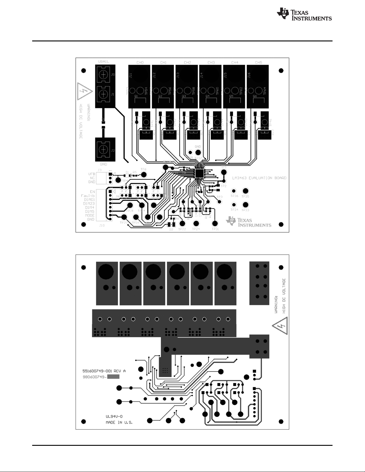
Board Layout
5 Board Layout
www.ti.com
Figure 2. Top Layer
Figure 3. Bottom Layer
4
AN-2255 LM3463 Evaluation Board SNVA642A–May 2012–Revised May 2013
Copyright © 2012–2013, Texas Instruments Incorporated
Submit Documentation Feedback
Page 5
Primary power supply
(e.g. AC/DC offline converter, DC power supply)
LM3463 EVALUATION
BOARD
WARNING:
HIGH DC
VOLTAGE
J0
J1
J11
J12
J13
J14
J15
J16
J2
J9J5J7
J4J6J8
J10
J3
CH0 CH1 CH2 CH3 CH4 CH5VRAIL
GND
2.5V
VFB
RVFB1
RVFB2
VRAIL
GND
VFB
LM3463 evaluation board
LED strings x 6
Default operation conditions of the board:
I
OUT
per channel: 200 mA
No. of LED per string: 14 (~3.2V forward voltage per LED)
LED turn on voltage: V
RAIL
= 48V
Dimming mode: Direct PWM dimming mode
@ 100% dimming duty
Assumed characteristics of the primary power supply:
VFB = 2.5V
RVFB1 = 39.8 k
RVFB2 = 3.9 k
www.ti.com
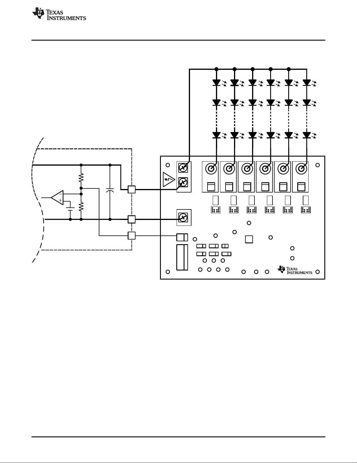
6 Connection Diagram
Connection Diagram
Figure 4. Connecting the LM3463 evaluation board to a primary power supply
7 Primary Power Supply
The LM3463 evaluation board is designed to operate with an external primary power supply. A primary
power supply can be any kind of DC power supply with an accessible output voltage feedback node. For
instance, either an AC/DC off-line power converter or a DC/DC switching converter can be used as a
primary power supply. The LM3463 evaluation board should connect to the primary power supply via three
terminals, the VRAIL, GND and VFB as shown in Figure 1.
The board includes three screw type connectors for high current connections, namely J0, J1 and J2. The
J1 and J2 should connect to the positive and GND output terminals of the primary power supply
accordingly with minimum of wire 18 AWG.
Generally, the board is designed to drive from one to six LED strings of 14 serial LEDs per string. The
driving current of each sting is set to 200 mA by default, thus assuming each LED carries a 3.2V forward
voltage, the maximum total output power of this evaluation board under steady state is about 54W.
Because the output voltage of the primary power supply, V
Control (DHC) circuit of the LM3463 to maintain maximum system efficiency, therefore the V
a wide and adjustable voltage range.
RAIL
is controlled by the Dynamic Headroom
must have
RAIL
SNVA642A–May 2012–Revised May 2013 AN-2255 LM3463 Evaluation Board
Submit Documentation Feedback
Copyright © 2012–2013, Texas Instruments Incorporated
5
Page 6
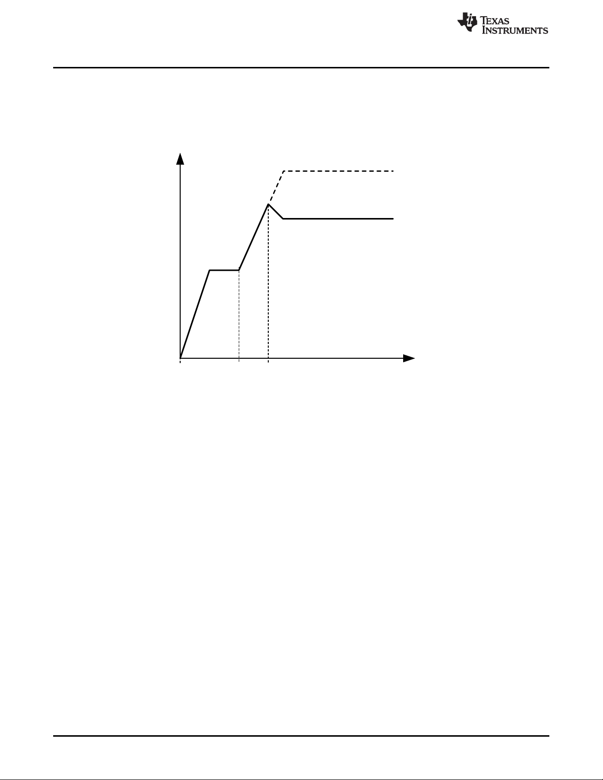
0
V
DHC_READY
V
RAIL(nom)
V
RAIL(steady)
V
RAIL(peak)
V
RAIL
Time
Pushed up
by LM3463
Initiated by
primary power
supply
DHC activated
Primary Power Supply
www.ti.com
Generally the required range of the V
voltages of the LED strings (respectively, V
is determined by the highest and lowest possible forward
RAIL
LED-MAX-COLD
and V
LED-MIN-HOT
). Since the forward voltage of the
LED strings varies according to the changing of the ambient temperature, the voltage for turning the LEDs
on at system startup must be set higher than the V
V
at system startup.
RAIL
LED-MAX-COLD
.Figure 5 shows the different voltage level of
Figure 5. Different voltage levels of the V
In Figure 5, the V
V
RAIL(peak)
is the highest level of V
is the output voltage of the primary power supply under the control of the LM3463.
RAIL
when the voltage of the OutP pin of the LM3463 equals 0V. V
RAIL
is the voltage level that the LM3463 turns all output channels on. V
at system startup
RAIL
RAIL(nom)
is the nominal output voltage of
the primary power supply when the OutP pin voltage is higher than VFB+0.6V (i.e. prior to DHC starting)
In order to secure sufficient rail voltage to maintain regulated LED currents when enabling the output
channels, the V
RAIL(peak)
and V
DHC_READY
must be set higher than V
LED-MAX-COLD
(the highest forward voltage of
the LED strings under low ambient temperature). The following settings are suggested to ensure correct
system startup sequence:
1. V
RAIL(nom)
2. V
DHC_READY
3. V
RAIL(peak)
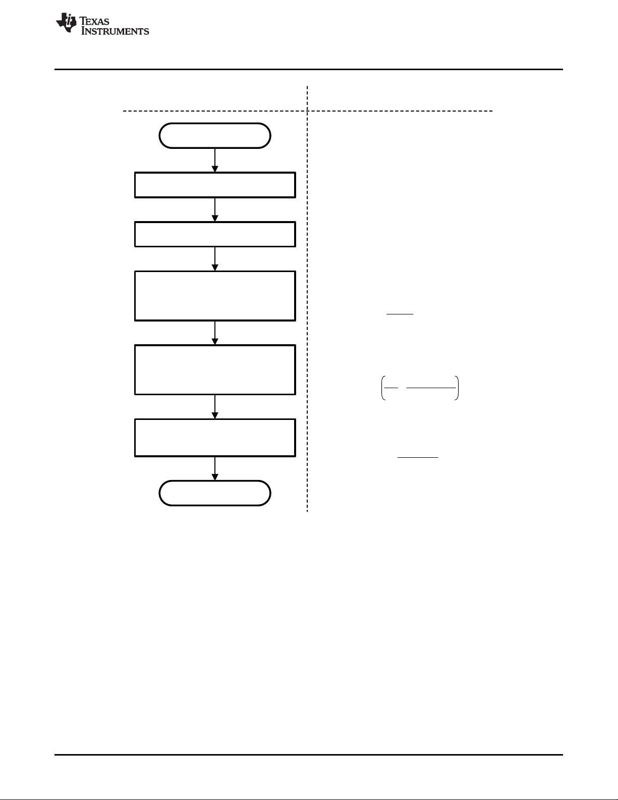
Figure 6 shows a suggested procedure to determine the V
= V
LED-MIN-HOT
= V
= V
LED-MAX-COLD
DHC_READY
- 5V
+ 5V
+ 5V
RAIL(nom)
, V
DHC_READY
and V
RAIL(peak)
.
DHC_READY
6
AN-2255 LM3463 Evaluation Board SNVA642A–May 2012–Revised May 2013
Copyright © 2012–2013, Texas Instruments Incorporated
Submit Documentation Feedback
Page 7
V
LED-MAX-COLD
, the highest forward
voltage of LED strings under low
temperature
Identify V
LED-MAX-COLD
Identify V
LED-MIN-HOT
Adjust the nominal output voltage of the
primary power supply,
V
RAIL(nom)
= V
LED-MIN-HOT
- 5V
Set the peak output voltage of the primary
power supply (at V
OutP
= 0.15V),
V
RAIL(peak)
= V
LED-MAX-COLD
+ 10V
Set the LED turn on voltage,
V
DHC_READY
= V
LED-MAX-COLD
+ 5V
Begin of design
End of design
V
LED-MIN-HOT
, the lowest forward voltage
of LED strings under high temperature
V
RAIL(nom)
, the nominal output voltage
of the primary power supply.
e.g. Assume V
FB
= 2.5V,
REMARKSPROCEDURES
V
RAIL(peak)
, the output voltage of the
primary power supply when the OutP
pin is pulling to its minimum.
R1 + R
2
R
2
2.5V x
V
RAIL(nom)
=
V
DHC_READY
, the LED turn on voltage is
defined by R
FB1
and R
FB2
connected to
the VLedFB pin.
R
FB1
+ R
FB2
R
FB2
2.5V +
V
DHC_READY
=
V
FB
R
2
V
FB
- 0.15 - 0.6
R
DHC
+ V
FB
R
1
xV
RAIL(peak)
=
+
www.ti.com
Primary Power Supply
Because the V
RAIL(peak)
turned on, the primary power supply must be able to deliver an output power no less than the total LED
current multiplied by the V
selecting a power supply for the LM3463 evaluation board. If the power supply is an off-the-shelf product,
the output voltage and value of the output voltage feedback resistor divider may need to be changed to
allow DHC.
Figure 6. Procedures of setting the rail voltage levels.
is the possible highest output voltage of the primary power supply with the LEDs
RAIL(peak)
. The flow chart in Figure 7 shows the recommended procedure of
SNVA642A–May 2012–Revised May 2013 AN-2255 LM3463 Evaluation Board
Submit Documentation Feedback
Copyright © 2012–2013, Texas Instruments Incorporated
7
Page 8

V
RAIL(peak)
is the highest output voltage
that the power converter needs to
deliver.
I
LEDx
is the forward current of an LED
string.
Determine:
I
LEDx
, V
RAIL(peak)
and V
RAIL(nom)
Prepare a power converter which has a
maximum output power > P
OUT(nom)
and a
maximum output voltage > V
RAIL(peak)
Adjust R1 and R2 to reduce the nominal
output voltage of the power converter to
V
RAIL(nom)
Begin of power
supply selection
The power converter must be able to
deliver a power no less than P
RAIL(peak)
even if the V
RAIL
is pushed to the
maximum by the LM3463, V
RAIL(peak)
REMARKSPROCEDURES
Adjust the value of R1 and R2 so as to
meet the equation:
V
FB
x
R
2
V
RAIL(nom)
=
Calculate the required maximum output
Power, P
RAIL(peak)
of the power supply
End of power
supply selection
x I
LEDx
No. of output ch.
P
RAIL(peak)
=
x V
RAIL(peak)
R1 + R
2
Response of the DHC Loop
www.ti.com
Going through the above procedures, the value of the R5, R2 and R4 are determined. The values of the
R5, R2 and R4 on the LM3463 evaluation board are 2.94 kΩ, 150 kΩ and 8.25 kΩ respectively. The
resistors may need replacing as needed to interface the board to a primary power supply.
8 Response of the DHC Loop
The cut-off frequency of the DHC loop f
The f
C(LM3463)
The default value of the C4 on the board is 1 uF which sets the cut-off frequency of the DHC loop to
0.1Hz.
In order to secure stable operation of the system, the cut-off frequency of the DHC loop of the LM3463
must be set lower than that of the primary power supply. Usually a DHC response of 1/10 of which of the
primary power supply is enough to secure stable operation. In the case where the primary power supply
has an unknown frequency response, the selection of the value of the C4 can be based on estimation.
Use a 1 uF ceramic capacitor as an initial value and reduce the value of C4 to increase the DHC loop
response as needed.
Figure 7. Procedure of selecting a primary power supply
C(LM3463)
is determined by the value of the external capacitor, C4.
is governed by the following equation.
(1)
8
AN-2255 LM3463 Evaluation Board SNVA642A–May 2012–Revised May 2013
Copyright © 2012–2013, Texas Instruments Incorporated
Submit Documentation Feedback
Page 9

0
V
DHC_READY
V
RAIL(nom)
V
LED
V
RAIL
Time
t
ST-1
t
ST-2
t
ST-3
t
ST-1
open
R
ISR
Startup time
t
ST-2
high
t
ST-3
low
V
IN-UVLO
6.67V
www.ti.com
9 Reducing the System Startup Time
The total system startup time is generally dependent on the frequency response of both the primary power
supply and DHC loop of the LM3463. The slower response of the two circuits, the longer time the system
takes to startup. Because the response of the primary is usually not user programmable, the overall
system startup time can be reduced by shortening the time for the V
V
DHC_READY
RISR, which governed by the following equation:
where
, namely the tST. as shown in Figure 8. The tSTis adjusted dependent on the value of the C4 and
Reducing the System Startup Time
to increase from V
RAIL
RAIL(nom)
to
(2)
(3)
Figure 8. Adjusting the tST with different value of RISR
The R9 on this evaluation board is opened by default, thus the system startup time is set to the longest.
The startup time of the board can be reduced by putting a 0603 resistor to the position of R9. The value of
the R9 should be no less than 130kΩ.
10 MOSFET Power Dissipation Limit
As the drain voltage of the MOSFETs (Q1, Q2, Q3, Q4, Q5 and Q6) exceeds four times the voltage of the
DRVLIM pin, the output currents are reduced to reduce the power dissipations on the MOSFETs. The
DRVLIM of the LM3463 of this evaluation board is connected to VCC via a 0Ω resistor, R37. Thus the
drain voltage threshold to perform MOSFET power dissipation limit is about 26.4V by default.
11 Analog Dimming Control
The reference voltage for the LED current regulators can be adjusted by changing the voltage at the
IOUTADJ pin of the LM3463. In this evaluation board, the reference voltage for current regulation is set to
200mV by connecting the IOUTADJ pin to VCC via a 0Ω resistor, R10. By default the pull-down resistor to
the IOUTADJ pin, R11 is opened. To adjust the IOUTADJ pin voltage, the R10 and R11 should be
replaced according to the required output current following the equation below:
SNVA642A–May 2012–Revised May 2013 AN-2255 LM3463 Evaluation Board
Submit Documentation Feedback
Copyright © 2012–2013, Texas Instruments Incorporated
9
Page 10

PWM Dimming Control
The IOUTADJ pin can be biased by a positive voltage in the range of 0V to 2.5V across the terminals
TP31and TP39. If the IOUTADJ pin is going to be biased by an external voltage source, the R10 and R11
should be removed.
12 PWM Dimming Control
The LM3463 evaluation board allows three different modes of PWM dimming control:
• Direct PWM Dimming Mode
• Serial Interface Mode
• DC Interface Mode
• The mode of PWM dimming control is selected by changing the position of the shunt jumper of J8.
Mode of dimming control Setting of J8
Direct PWM dimming mode Short Pos. 2–3
Serial interface mode Open
DC interface mode Short Pos. 1–2
Using PWM dimming control, the six output channels of the board are grouped into four individual groups
which are controlled by four individual PWM signals at the terminals TP12, TP14, TP16 and TP18.
www.ti.com
(4)
Terminal Involved channels
TP12 CH0, CH1
TP14 CH2, CH3
TP16 CH4
TP18 CH5
The terminals J4, J5, J6 and J7 are used to connect the DIM01(TP12), DIM23(TP14), DIM4(TP16) and
DIM5(TP18) pins of the LM3463 to either VCC or GND. The jumpers on these terminals should be
removed if external dimming control signals are applied to the board.
Direct PWM Dimming Mode
In the direct PWM dimming mode, the board accepts standard active high TTL level PWM signals to
perform dimming control. The minimum on duty is generally limited by the gate capacitance of the external
MOSFETs. Normally, an 8 µs minimum on time is suggested.
Serial Interface Mode
In the serial interface mode, the on duty of each output channel is controlled by a data byte of 8 bits wide.
In this mode the terminals TP12, TP14 and TP16 on the board comprise a serial data interface to receive
data bytes from external data source. The connection to the DIM5 pin is not used and should be
connected to GND by shortening the pins 2 and 3 of J7. The functions of the TP12, TP14 and TP16 in the
serial interface mode are as listed in the following table:
Serial Interface Mode
Terminal Function
TP12 Serial data input
TP14 Clock signal input
TP16 End Of data Frame (EOF) signal input
10
AN-2255 LM3463 Evaluation Board SNVA642A–May 2012–Revised May 2013
Copyright © 2012–2013, Texas Instruments Incorporated
Submit Documentation Feedback
Page 11
BIT7BIT6BIT5BIT4BIT3BIT2BIT1BIT0
One data byte
DIM01
DIM23
(Clock signal)
(Data)
DIM01
DIM23
(Clock signal)
(Data)
BYTE1
(Group D)
BYTE2
(Group C)
BYTE3
(Group B)
BYTE4
(Group A)
DIM4
(End of Frame)
EOF
One data frame
LSB MSB
BOF
www.ti.com
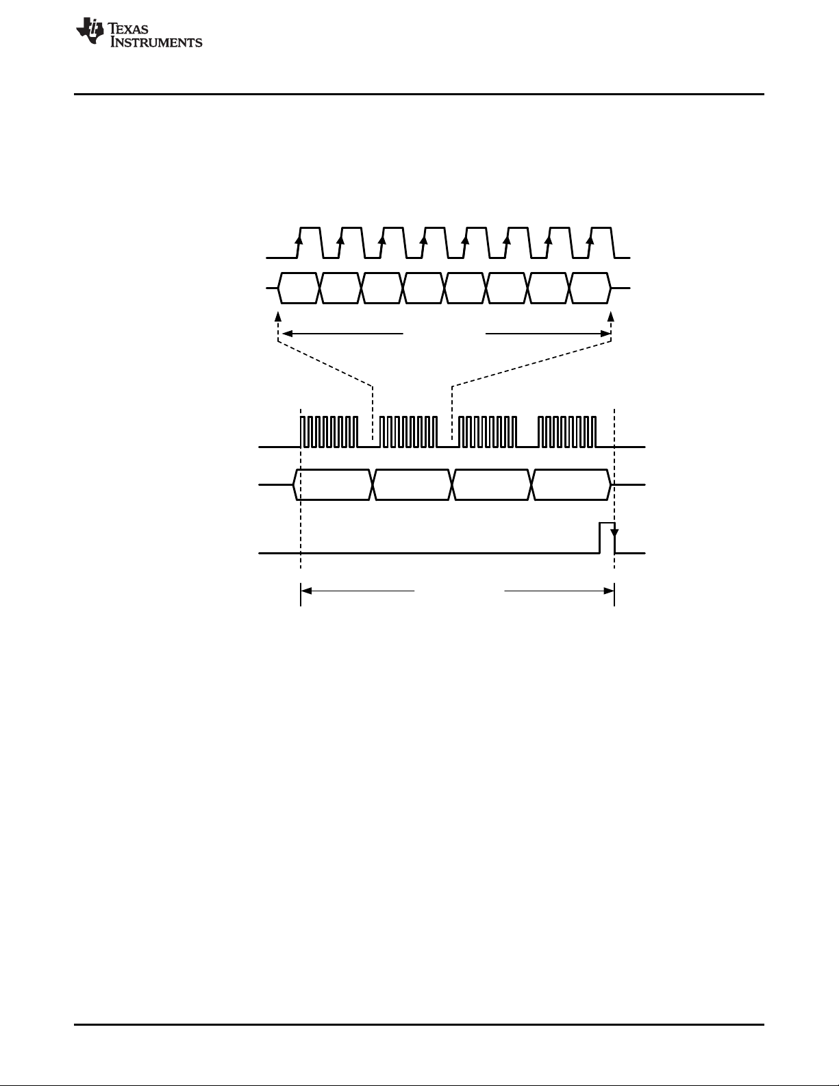
In the serial interface mode the LM3463 evaluation board accepts a data frame which consists of four data
bytes to control the on duty of the four groups of output channels via the terminal TP12 (DIM01). Every
data byte contains 8 bits in LSB (Least Significant Bit) first ordering and is clocked into the data buffer of
the LM3463 at every rising edge of clock signal at the terminal TP14 (DIM23). Every time a data frame is
clocked in to the LM3463 the terminal TP16 (DIM4) should be pulled low to generate a falling edge to
indicate an ‘End-Of-Frame (EOF)’. Figure 9 shows the typical waveform of a data frame and the
corresponding clock and EOF signals.
PWM Dimming Control
Figure 9. Typical waveforms of a complete data frame in the serial interface mode
SNVA642A–May 2012–Revised May 2013 AN-2255 LM3463 Evaluation Board
Submit Documentation Feedback
Copyright © 2012–2013, Texas Instruments Incorporated
11
Page 12

Input Data Code
(Decimal)
3/256
PWM dimming duty
4/256
5/256
0
6/256
32415
254
253
255
252
0
256/256
251
255/256
254/256
253/256
252/256
2/256
(Skipped)1/256
PWM Dimming Control
www.ti.com
Figure 10. PWM dimming duty vs code value of a data byte
In the serial interface mode, the six output channels are grouped into four individual groups. The on duty
of each group is controlled by the value of a specific data byte as listed in the following table:
Output channel Data byte
CH0, CH1 BYTE1
CH2, CH3 BYTE2
CH4 BYTE3
CH5 BYTE4
Because the data width of a data byte is fixed to 8 bits, the step size of the LED current is equal to 1/256
of the full scale current. To allow the use of 0% on duty, the steps 1 and 2 are combined to give a 2/256
on duty. Thus either applying a hexadecimal code 001h or 002h the LM3463 will give a 2/256 on duty. The
dimming duty in the serial interface mode is governed by the following equation:
(5)
Figure 10 shows the relationship of the code value of a data byte and PWM dimming duty.
DC Interface Mode
In the DC interface mode, the on duty of the output channels are adjusted according to the voltage on the
terminals TP12, TP14, TP16 and TP20. In this mode, the six output channels are grouped into four groups
and controlled by the voltage on four terminals individually as listed in the following table:
12
AN-2255 LM3463 Evaluation Board SNVA642A–May 2012–Revised May 2013
Copyright © 2012–2013, Texas Instruments Incorporated
Submit Documentation Feedback
Page 13

Analog voltage
at the DIMn pin
2/256
PWM dimming duty
3/256
4/256
0
5/256
5
.
7
V-V
LSB
5
.
7
V-2
V
LSB
5
.
7
V
5
.
7
V
-
3
V
LSB
256/256
5
.
7
V-4
V
LSB
255/256
254/256
253/256
252/256
0
.
8
V
+
3
V
LSB
0
.
8
V
+
2
V
LSB
0
.
8
V
+
4
V
LSB
0
.
8
V
+
V
LSB
0
.
8
V
6/256
V
LSB
=
5.7V - 0.8V
256
(Skipped) 1/256
www.ti.com
The voltage being applied to the terminals should be in the range of 0.8V to 5.7V. The dimming duty in the
DC interface mode is governed by the following equation:
In this mode, the conversion of analog voltage to dimming duty is accomplished by an internal 8-bit ADC
of the LM3463, thus the step size of the LED current is equal to 1/256 of the full scale current. To allow
the use of 0% on duty, the steps 1 and 2 are combined to give a 2/256 on duty. Thus either applying a
voltage in the range of 0.8V to 0.8V+V
Figure 11 shows the Conversion characteristics of the analog voltage to PWM dimming control circuit:
Disabling Output Channel(s)
Output channel Terminal
CH0, CH1 TP12
CH2, CH3 TP14
CH4 TP16
CH5 TP18
to the dimming control inputs will result in a 2/256 on duty.
LSB
(6)
Figure 11. Conversion characteristic of the analog voltage to PWM dimming control circuit
13 Disabling Output Channel(s)
An output channel of this evaluation board can be disabled by not connecting an LED string to the output
terminal. A disabled channel is excluded from the DHC loop and remained in OFF state until a falling edge
at the EN pin or system repower is applied. The channel 0 must be used regardless of the number of
disabled channel.
SNVA642A–May 2012–Revised May 2013 AN-2255 LM3463 Evaluation Board
Submit Documentation Feedback
Copyright © 2012–2013, Texas Instruments Incorporated
13
Page 14
LM3463 EVALUATION BOARD
WARNING:
HIGH DC VOLTAGE
J0
J1
J11
J12
J13
J14
J15
J16
J2
J9J5J7
J4J6J8
J10
J3
CH0 CH1 CH2 CH3 CH4 CH5VRAIL
GND
LM3463 EVALUATION BOARD
WARNING:
HIGH DC VOLTAGE
J0
J1
J11
J12
J13
J14
J15
J16
J2
J9J5J7
J4J6J8
J10
J3
CH0 CH1 CH2 CH3 CH4 CH5VRAIL
GND
LM3463 EVALUATION BOARD
WARNING:
HIGH DC VOLTAGE
J0
J1
J11
J12
J13
J14
J15
J16
J2
J9J5J7
J4J6J8
J10
J3
CH0 CH1 CH2 CH3 CH4 CH5VRAIL
GND
TP12
TP14
TP33
TP35
VFB
TP12
TP14
TP33
TP35
VFB
J4 = OPEN J7 = SHORT 2-3
J5 = OPEN J8 = OPEN
J6 = OPEN J9 = OPEN
TP22
TP3
TP22
TP3
TP22
TP3
MASTER
J4 = OPEN J7 = SHORT 2-3
J5 = OPEN J8 = OPEN
J6 = SHORT 2-3 J9 = OPEN
VLedFB = VCC
R2 = OPEN
R4 = OPEN
SLAVE 1
J4 = OPEN J7 = SHORT 2-3
J5 = OPEN J8 = OPEN
J6 = SHORT 2-3 J9 = OPEN
VLedFB = VCC
R2 = OPEN
R4 = OPEN
SLAVE 2
LED array 1 LED array 2 LED array 3VRAIL
GND
VFB
Primary Power Supply
TP12
TP14
TP16
LOAD
SCLK
SDAT
Interface to MCU for
dimming control
Cascading the LM3463 evaluation board
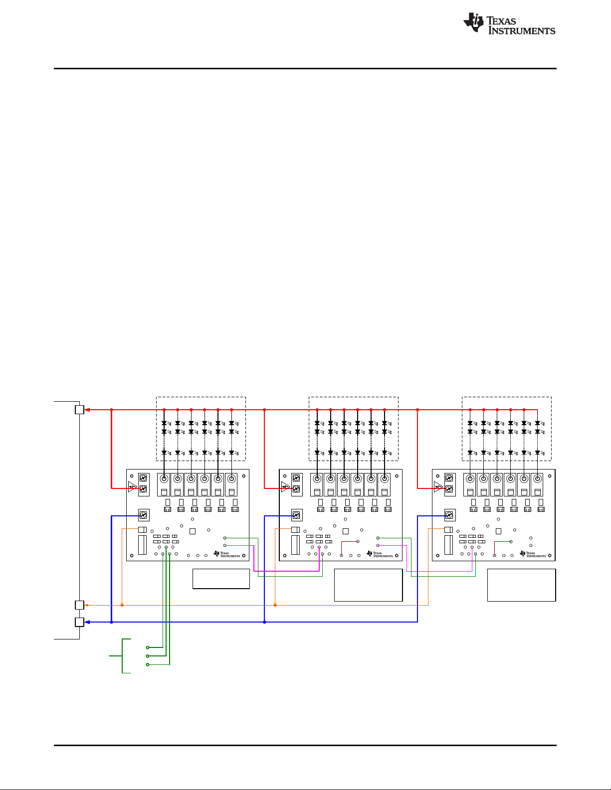
14 Cascading the LM3463 evaluation board
A number of the LM3463 evaluation boards can be cascaded to expand the number of output channels.
The connection among boards differs depending on the selected mode for dimming control. The
connection diagrams for the serial interface mode, DC interface mode and direct PWM mode are as
illustrated in the Figure 12, Figure 13, and Figure 14, respectively.
When a number of the LM3463 evaluation boards are cascaded, one of the boards must be set as master
unit and the other boards must be set as slave units. The master unit is the board which has the VFB
terminal connected to the primary power supply. The master unit controls the system startup time and
distributes dimming control signals to the slave units, the connections among the boards differs depending
on the mode of dimming control being selected.
By default, the LM3463 evaluation board is set as a master unit in direct PWM dimming mode with 100%
on duty. To set a board to be a slave unit, the resistors R2 and R4 must be removed and the terminal TP3
(VLedFB pin of the LM3463) should be connected to the terminal TP22 (VCC pin of the LM3463) using an
external connection.
In cascade operation, the number of slave units is virtually unlimited. However, in high power applications
the accumulated voltage drop on the power return part could impair the function of the DHC. Generally it
is suggested not to cascade more than four pieces of the LM3463 evaluation board to secure stable
system operation.
15 PCB Design
Good heat dissipation helps optimize the performance of the LM3463. The ground plane should be used
to connect the exposed pad of the LM3463, which is internally connected to the LM3463 die substrate.
The area of the ground plane should be extended as much as possible on the same copper layer around
the LM3463. Using numerous vias beneath the exposed pad to dissipate heat of the LM3463 to another
copper layer is also a good practice.
www.ti.com
14
Figure 12. A 12 channel lighting system using serial interface mode for dimming control
AN-2255 LM3463 Evaluation Board SNVA642A–May 2012–Revised May 2013
Copyright © 2012–2013, Texas Instruments Incorporated
Submit Documentation Feedback
Page 15

LM3463 EVALUATION BOARD
WARNING:
HIGH DC VOLTAGE
J0
J1
J11
J12
J13
J14
J15
J16
J2
J9J5J7
J4J6J8
J10
J3
CH0 CH1 CH2 CH3 CH4 CH5VRAIL
GND
LM3463 EVALUATION BOARD
WARNING:
HIGH DC VOLTAGE
J0
J1
J11
J12
J13
J14
J15
J16
J2
J9J5J7
J4J6J8
J10
J3
CH0 CH1 CH2 CH3 CH4 CH5VRAIL
GND
LM3463 EVALUATION BOARD
WARNING:
HIGH DC VOLTAGE
J0
J1
J11
J12
J13
J14
J15
J16
J2
J9J5J7
J4J6J8
J10
J3
CH0 CH1 CH2 CH3 CH4 CH5VRAIL
GND
TP33
TP35
VFB
TP33
TP35
VFB
J4 = OPEN J7 = OPEN
J5 = OPEN J8 = SHORT 2-3
J6 = OPEN J9 = OPEN
TP22
TP3
TP22
TP3
TP22
TP3
MASTER
J4 = OPEN J7 = OPEN
J5 = OPEN J8 = SHORT 2-3
J6 = OPEN J9 = OPEN
VLedFB = VCC
R2 = OPEN
R4 = OPEN
SLAVE 1
J4 = OPEN J7 = OPEN
J5 = OPEN J8 = SHORT 2-3
J6 = OPEN J9 = OPEN
VLedFB = VCC
R2 = OPEN
R4 = OPEN
SLAVE 2
LED array 1 LED array 2 LED array 3VRAIL
GND
VFB
Primary Power Supply
TP12
TP14
TP16
DIM4
DIM23
DIM01
Logic level PWM
dimming control
signals
TP18
DIM5
TP12
TP14
TP16
TP18
TP12
TP14
TP16
TP18
LM3463 EVALUATION BOARD
WARNING:
HIGH DC VOLTAGE
J0
J1
J11
J12
J13
J14
J15
J16
J2
J9J5J7
J4J6J8
J10
J3
CH0 CH1 CH2 CH3 CH4 CH5VRAIL
GND
LM3463 EVALUATION BOARD
WARNING:
HIGH DC VOLTAGE
J0
J1
J11
J12
J13
J14
J15
J16
J2
J9J5J7
J4J6J8
J10
J3
CH0 CH1 CH2 CH3 CH4 CH5VRAIL
GND
LM3463 EVALUATION BOARD
WARNING:
HIGH DC VOLTAGE
J0
J1
J11
J12
J13
J14
J15
J16
J2
J9J5J7
J4J6J8
J10
J3
CH0 CH1 CH2 CH3 CH4 CH5VRAIL
GND
TP12
TP14
TP33
TP35
VFB
TP12
TP14
TP33
TP35
VFB
J4 = OPEN J7 = OPEN
J5 = OPEN J8 = SHORT 1-2
J6 = OPEN J9 = OPEN
TP22
TP3
TP22
TP3
TP22
TP3
MASTER
J4 = OPEN J7 = SHORT 2-3
J5 = OPEN J8 = SHORT 1-2
J6 = SHORT 2-3 J9 = OPEN
VLedFB = VCC
R2 = OPEN
R4 = OPEN
SLAVE 1
J4 = OPEN J7 = SHORT 2-3
J5 = OPEN J8 = SHORT 1-2
J6 = SHORT 2-3 J9 = OPEN
VLedFB = VCC
R2 = OPEN
R4 = OPEN
SLAVE 2
LED array 1 LED array 2 LED array 3VRAIL
GND
VFB
Primary Power Supply
TP12
TP14
TP16
VDIM4
VDIM23
VDIM01
DC voltages for
dimming control
TP18
VDIM5
www.ti.com
PCB Design
Figure 13. A 12 channel lighting system using DC interface mode for dimming control
Figure 14. A 12 channel lighting system using Direct PWM mode for dimming control
SNVA642A–May 2012–Revised May 2013 AN-2255 LM3463 Evaluation Board
Submit Documentation Feedback
Copyright © 2012–2013, Texas Instruments Incorporated
15
Page 16

Typical Waveforms
16 Typical Waveforms
All curves taken at VIN= 48V with configuration in typical application for driving twelve power LEDs with six
output channels active and 200 mA output current per channel. TA= 25°C, unless otherwise specified.
Figure 15. Direct PWM Dimming Mode Figure 16. DC Interface Mode
250Hz 50% dimming duty at DIMn pin 10Hz 3V to 2V ramp at DIMn pin
www.ti.com
16
Figure 17. PWM dimming Figure 18. PWM dimming
I
delay at V
OUTn
Figure 19. I
I
OUTn
OUTn
AN-2255 LM3463 Evaluation Board SNVA642A–May 2012–Revised May 2013
rising I
DIMn
delay at V
OUTn
ch-ch delay Figure 20. I
rising I
Copyright © 2012–2013, Texas Instruments Incorporated
falling
DIMn
ch-ch delay
OUTn
falling
OUTn
Submit Documentation Feedback
Page 17

IMPORTANT NOTICE
Texas Instruments Incorporated and its subsidiaries (TI) reserve the right to make corrections, enhancements, improvements and other
changes to its semiconductor products and services per JESD46, latest issue, and to discontinue any product or service per JESD48, latest
issue. Buyers should obtain the latest relevant information before placing orders and should verify that such information is current and
complete. All semiconductor products (also referred to herein as “components”) are sold subject to TI’s terms and conditions of sale
supplied at the time of order acknowledgment.
TI warrants performance of its components to the specifications applicable at the time of sale, in accordance with the warranty in TI’s terms
and conditions of sale of semiconductor products. Testing and other quality control techniques are used to the extent TI deems necessary
to support this warranty. Except where mandated by applicable law, testing of all parameters of each component is not necessarily
performed.
TI assumes no liability for applications assistance or the design of Buyers’ products. Buyers are responsible for their products and
applications using TI components. To minimize the risks associated with Buyers’ products and applications, Buyers should provide
adequate design and operating safeguards.
TI does not warrant or represent that any license, either express or implied, is granted under any patent right, copyright, mask work right, or
other intellectual property right relating to any combination, machine, or process in which TI components or services are used. Information
published by TI regarding third-party products or services does not constitute a license to use such products or services or a warranty or
endorsement thereof. Use of such information may require a license from a third party under the patents or other intellectual property of the
third party, or a license from TI under the patents or other intellectual property of TI.
Reproduction of significant portions of TI information in TI data books or data sheets is permissible only if reproduction is without alteration
and is accompanied by all associated warranties, conditions, limitations, and notices. TI is not responsible or liable for such altered
documentation. Information of third parties may be subject to additional restrictions.
Resale of TI components or services with statements different from or beyond the parameters stated by TI for that component or service
voids all express and any implied warranties for the associated TI component or service and is an unfair and deceptive business practice.
TI is not responsible or liable for any such statements.
Buyer acknowledges and agrees that it is solely responsible for compliance with all legal, regulatory and safety-related requirements
concerning its products, and any use of TI components in its applications, notwithstanding any applications-related information or support
that may be provided by TI. Buyer represents and agrees that it has all the necessary expertise to create and implement safeguards which
anticipate dangerous consequences of failures, monitor failures and their consequences, lessen the likelihood of failures that might cause
harm and take appropriate remedial actions. Buyer will fully indemnify TI and its representatives against any damages arising out of the use
of any TI components in safety-critical applications.
In some cases, TI components may be promoted specifically to facilitate safety-related applications. With such components, TI’s goal is to
help enable customers to design and create their own end-product solutions that meet applicable functional safety standards and
requirements. Nonetheless, such components are subject to these terms.
No TI components are authorized for use in FDA Class III (or similar life-critical medical equipment) unless authorized officers of the parties
have executed a special agreement specifically governing such use.
Only those TI components which TI has specifically designated as military grade or “enhanced plastic” are designed and intended for use in
military/aerospace applications or environments. Buyer acknowledges and agrees that any military or aerospace use of TI components
which have not been so designated is solely at the Buyer's risk, and that Buyer is solely responsible for compliance with all legal and
regulatory requirements in connection with such use.
TI has specifically designated certain components as meeting ISO/TS16949 requirements, mainly for automotive use. In any case of use of
non-designated products, TI will not be responsible for any failure to meet ISO/TS16949.
Products Applications
Audio www.ti.com/audio Automotive and Transportation www.ti.com/automotive
Amplifiers amplifier.ti.com Communications and Telecom www.ti.com/communications
Data Converters dataconverter.ti.com Computers and Peripherals www.ti.com/computers
DLP® Products www.dlp.com Consumer Electronics www.ti.com/consumer-apps
DSP dsp.ti.com Energy and Lighting www.ti.com/energy
Clocks and Timers www.ti.com/clocks Industrial www.ti.com/industrial
Interface interface.ti.com Medical www.ti.com/medical
Logic logic.ti.com Security www.ti.com/security
Power Mgmt power.ti.com Space, Avionics and Defense www.ti.com/space-avionics-defense
Microcontrollers microcontroller.ti.com Video and Imaging www.ti.com/video
RFID www.ti-rfid.com
OMAP Applications Processors www.ti.com/omap TI E2E Community e2e.ti.com
Wireless Connectivity www.ti.com/wirelessconnectivity
Mailing Address: Texas Instruments, Post Office Box 655303, Dallas, Texas 75265
Copyright © 2013, Texas Instruments Incorporated
 Loading...