

Page 1

1 Introduction
The LM3450A evaluation board is designed to provide an AC to LED solution for a 30W LED load.
Specifically, it takes an AC mains input and converts it to a constant current output of 700mA for a series
string of 1 to 13 LEDs (maximum LED stack voltage of 45V). There are two assembly versions designed
to operate from two different nominal AC input voltages, 120VACor 230VAC. .
The board employs a two stage design with an LM3450A flyback primary stage and an LM3409HV
secondary stage. The LM3450A provides an isolated 50V regulated output voltage and a power factor
corrected input current. The LM3409HV uses the 50V flyback output as its input and provides a constant
current of 700mA to the LED load. This two stage design provides excellent line and load regulation as
well as isolation. The board is comprised of two copper layers with components on both sides and an FR4
dielelctric.
The two-stage design has several key advantages over a single stage design including:
• No 120Hz LED current ripple
• Better dimming performance at low dimming levels.
• Better line disturbance rejection
• Better efficiency using small LED stack voltages
User's Guide
SNVA485B–June 2011–Revised May 2013
AN-2150 LM3450A Evaluation Board
2 Specifications
120VAC30W Version
• Input Voltage Range: VIN= 90VAC– 135V
• Regulated Flyback Output Voltage: V
• Maximum LED Stack Voltage: V
• Regulated LED Current: I
230VAC30W Version
• Input Voltage Range: VIN= 180VAC– 265V
• Regulated Flyback Output Voltage: V
• Maximum LED Stack Voltage: V
• Regulated LED Current: I
= 700mA
LED
= 700mA
LED
LED
LED
OUT
< 45V
OUT
< 45V
AC
= 50V
AC
= 50V
All trademarks are the property of their respective owners.
SNVA485B–June 2011–Revised May 2013 AN-2150 LM3450A Evaluation Board
Submit Documentation Feedback
Copyright © 2011–2013, Texas Instruments Incorporated
1
Page 2
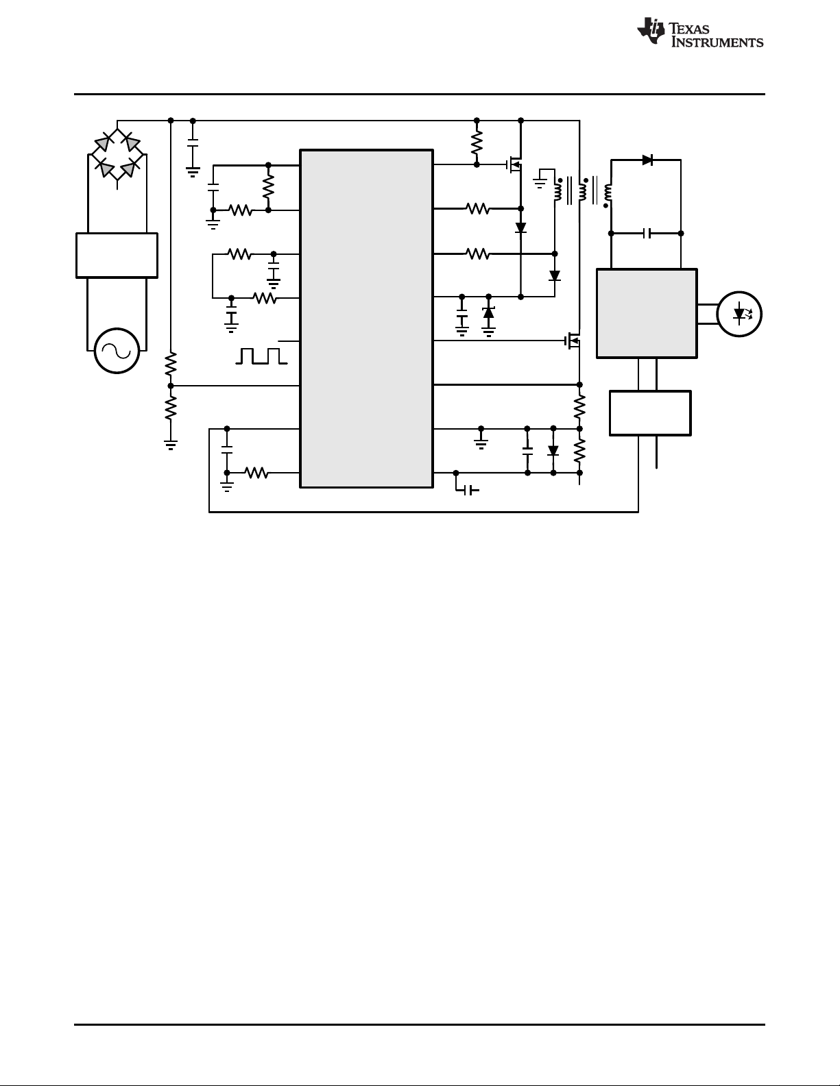
ZCD
GATE
LM3450A
GND
COMP
FB
HOLD
CS
DIM
FLT2
FLT1
PWM
BIAS
RETURN
OPTICAL
ISOLATION
RETURN
EMI FILTER
PWM
AC
INPUT
LED
LOAD
V
CC
V
AC
I
SEN
V
REF
V
ADJ
HOLD
LM3409HV
LED Driver
Specifications
www.ti.com
Figure 1. Schematic
2
AN-2150 LM3450A Evaluation Board SNVA485B–June 2011–Revised May 2013
Copyright © 2011–2013, Texas Instruments Incorporated
Submit Documentation Feedback
Page 3
P
OUT
(W)
PF
1.00
0.98
0.96
0.94
0.92
16 20 24 28 32
100 V
AC
120 V
AC
P
OUT
(W)
PF
1.00
0.98
0.96
0.94
0.92
16 20 24 28 32
200 V
AC
230 V
AC
P
OUT
(W)
EFFICIENCY (%)
84
82
80
78
76
16 20 24 28 32
100 V
AC
120 V
AC
P
OUT
(W)
EFFICIENCY (%)
84
82
80
78
76
16 20 24 28 32
200 V
AC
230 V
AC
www.ti.com
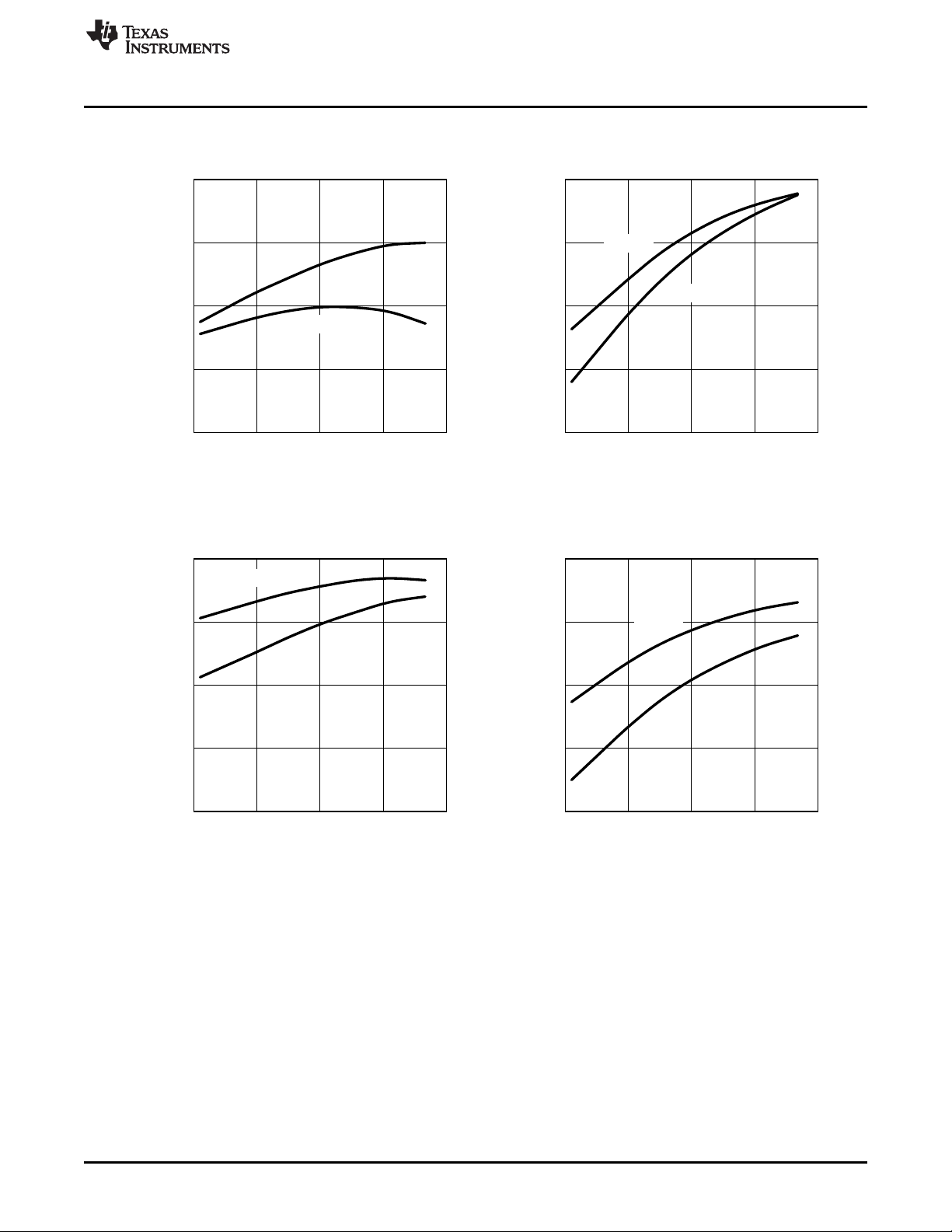
3 Typical Performance
Figure 2. 120V, 30W Version Figure 3. 230V, 30W Version
Efficiency vs. Output Power Efficiency vs. Output Power
Typical Performance
Figure 4. 120V, 30W Version Figure 5. 230V, 30W Version
Power Factor vs. Output Power Power Factor vs. Output Power
SNVA485B–June 2011–Revised May 2013 AN-2150 LM3450A Evaluation Board
Submit Documentation Feedback
3
Copyright © 2011–2013, Texas Instruments Incorporated
Page 4
0
20
40
60
80
100
1 3 5 7 9 11 13 15 17 19 21 23 25 27 29 31 33 35 37 39
AMPLITUDE (mA)
HARMONIC NUMBER
Limits
Measured
0
10
20
30
40
50
1 3 5 7 9 11 13 15 17 19 21 23 25 27 29 31 33 35 37 39
AMPLITUDE (mA)
HARMONIC NUMBER
Limits
Measured
AMPLITUDE in dbuV
FREQUENCY
AMPLITUDE in dbuV
FREQUENCY
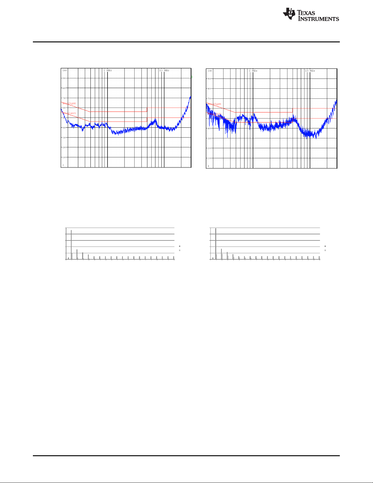
Conducted EMI Performance
4 Conducted EMI Performance
Figure 6. 120V, 30W Conducted EMI Peak Scan Figure 7. 230V, 30W Conducted EMI Peak Scan
Line and Neutral - CISPR/FCC Class B Quasi Peak and Line and Neutral - CISPR/FCC Class B Quasi Peak and
Average Limits Average Limits
5 THD / Harmonic Performance
www.ti.com
Figure 8. 120V, 30W THD Measurements Figure 9. 230V, 30W THD Measurements
EN 61000-3 Class C Limits EN 61000-3 Class C Limits
THD = 6.27% ; Fundamental = 316mA THD = 8.96% ; Fundamental = 167mA
4
AN-2150 LM3450A Evaluation Board SNVA485B–June 2011–Revised May 2013
Copyright © 2011–2013, Texas Instruments Incorporated
Submit Documentation Feedback
Page 5
V
CC
V
REF
ZCDFLT2
DIM GATE
V
AC
CS
COMP GND
FB I
SEN
HOLDV
ADJ
FLT1
BIAS
9
10
11
12
13
14
15
16
8
7
6
5
4
3
2
1
www.ti.com
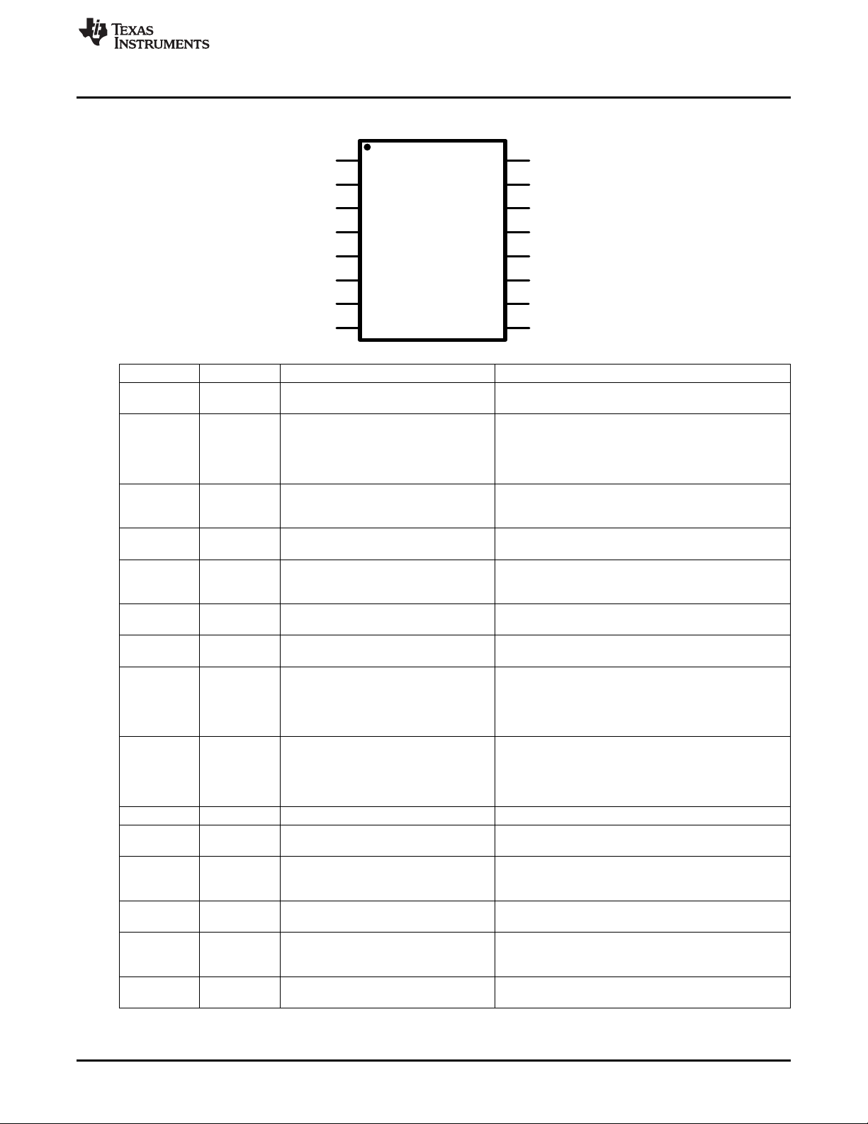
6 LM3450A Pin Descriptions
SNVA485B–June 2011–Revised May 2013 AN-2150 LM3450A Evaluation Board
Submit Documentation Feedback
LM3450A Pin Descriptions
Pin Name Description Application Information
1 V
REF
3V Reference
Reference Output: Connect directly to V
divider feeding V
and to necessary external circuits.
ADJ
Analog Dim and Phase Dimming Range Input: Connect
2 V
ADJ
Analog Adjust range. Connect to resistor divider from V
directly to V
usable range of some phase dimmers or for analog
to force standard 70% phase dimming
REF
dimming. Connect to GND for low power mode.
Ramp Comparator Input: Connect a series resistor from
3 FLT2 Filter 2 FLT1 capacitor and a capacitor to GND to establish
second filter pole.
4 FLT1 Filter 1
Angle Decoder Output: Connect a series resistor to a
capacitor to ground to establish first filter pole.
Open Drain PWM Dim Output: Connect to dimming input
5 DIM 500 Hz PWM Output of output stage LED driver (directly or with isolation) to
provide decoded dimming command.
6 V
AC
Sampled Rectified Line
7 COMP Compensation
Multiplier and Angle Decoder Input: Connect to resistor
divider from rectified AC line.
Error Amplifier Output and PWM Comparator Input:
Connect a capacitor to GND to set the compensation.
Error Amplifier Inverting Input: Connect to output voltage
via resistor divider to control PFC voltage loop for non-
8 FB Feedback isolated designs. Connect to a 5.11kΩ resistor to GND
for isolated designs (bypasses error amplifier). Also
includes over-voltage protection and shutdown modes.
Input Current Sense Non-Inverting Input: Connect to
diode bridge return and resistor to GND to sense input
9 I
SEN
Input Current Sense current for dynamic hold. Connect a 0.1µF capacitor and
Schottky diode to GND, and a 0.22µF capacitor to
HOLD.
10 GND Power Ground System Ground
11 CS Current Sense
MosFET Current Sense Input: Connect to positive
terminal of sense resistor in PFC MosFET source.
Gate Drive Output: Connect to gate of main power
12 GATE Gate Drive MosFET for PFC.Gate Drive Output: Connect to gate of
main power MosFET for PFC.
13 V
14 ZCD Zero Crossing Detector transformer/inductor winding to detect when all energy
15 HOLD Dynamic Hold
CC
Copyright © 2011–2013, Texas Instruments Incorporated
Input Supply
Power Supply Input: Connect to primary bias supply.
Connect a 0.1µF bypass capacitor to ground.
Demagnetization Sense Input: Connect a resistor to
has been transferred.
Open Drain Dynamic Hold Input: Connect to holding
resistor which is connected to source of passFET.
or to resistor
ADJ
to extend
REF
5
Page 6
UVLO
1
CSP
2
VIN
3
4
8
COFF
7
EN
6
CSN
5
9
10
GND PGATE
DAP
VCC
IADJ
LM3409HV Pin Descriptions
Pin Name Description Application Information
16 BIAS Pre-regulator Gate Bias passFET and to resistor to rectified AC (drain of
7 LM3409HV Pin Descriptions
Pin Name Description Application Information
1 UVLO Input Under Voltage Lock-out 1.24V and hysteresis is provided by a 22µA current
2 I
3 EN Logic Level Enable
4 COFF Off-time programming
5 GND Power Ground Connect to the system ground.
6 PGATE Gate Drive Connect to the gate of the external PFET.
7 CSN Negative Current Sense Connect to the negative side of the sense resistor.
8 CSP Positive Current Sense
9 V
10 V
DAP DAP Thermal PAD on bottom of IC
ADJ
CC
IN
VIN-referenced Linear Regulator Output
www.ti.com
Pre-regulator Gate Bias Output: Connect to gate of
passFET) to aid with startup.
Connect to a resistor divider from VIN. UVLO threshold is
source.
Apply a voltage between 0 - 1.24V, or connect a resistor
Analog LED Current Adjust from this pin to GND, to set the current sense threshold
voltage.
Apply a voltage >1.6V to enable device, a PWM signal
to dim, or a voltage <0.6V for low power shutdown.
Connect an external resistor from VOto this pin, and a
capacitor from this pin to GND to set the off-time.
Connect to the positive side of the sense resistor (also
connected to VIN).
Connect at least a 1 µF ceramic capacitor from this pin
to CSN. The regulator provides power for P-FET drive.
Input Voltage Connect to the input voltage.
Connect to pin 5 (GND). Place 4-6 vias from DAP to
bottom layer GND plane.
6
AN-2150 LM3450A Evaluation Board SNVA485B–June 2011–Revised May 2013
Copyright © 2011–2013, Texas Instruments Incorporated
Submit Documentation Feedback
Page 7

ZCD
GATE
LM3450A
V
CC
GND
COMP
FB
HOLD
V
AC
V
ADJ
CS
DIM
FLT2
FLT1
I
SEN
PWM
V
REF
BIAS
IADJ
EN
CSN
LM3409HV
UVLO
VCC
COFF
GND
CSP
PGATE
DAP
VIN
V
OUT
PWM
V
OP1
V
OP2
RETURN
RETURN
V
LED
LMV431
OPTO1
OPTO2
V
OP2
V
OP1
V
POP2
V
OUT
EMI
FILTER
CONTROL
FEEDBACK
SECONDARY
LED DRIVER
DIMMING
VREF
+
-
AC
MAINS
LED
LOAD
Q1
Q3
D10
D23
D8
D9
D4
C8
C9
C30
C7
C1
C2
C3
C66
C26
C11
C13
C4
C5
D5
D1
C42
C44
D16
C43
C17
C18
C24
C23
D17
C22
L1
L2
T1
R8
R9
R56
R2
R3
R47
D6
R5
R7
R17
R23
R24
R25
R26
R29
R32
R38
R30
R31
R34
R36
R70
R77
R72
R81
R16
R71
R84
R65
R66
R83
R58
R1
C35
C34
C38
C36
C39
C37
C47
D15
D13
D14
D22
D11D12
Q7
L3
Q6
Q2
R57
HOLD
V
LED
R39
D7
D2
D3
U9
U8
U10
U1
U11
V
POP2
V
CC
R18
Q8
D18
C21
C46
L4
V
CC
V
ADJ
COMPBIAS
D21
D24
R20
Q4
R21
SOFTSTART
C12
D20
THERMAL
PROTECT
R10
R12
R14
R15
AUX
R6
AUX
R11
www.ti.com
8 Simplified Evaluation Board Schematic
Simplified Evaluation Board Schematic
SNVA485B–June 2011–Revised May 2013 AN-2150 LM3450A Evaluation Board
Submit Documentation Feedback
Figure 10. Simplified Evaluation Board Schematic
Copyright © 2011–2013, Texas Instruments Incorporated
7
Page 8
VREF
+
-
LM3450A FLYBACK
+
VREF
+
-
EMI + BRIDGE
LM3409HV BUCK
Design Information
9 Design Information
The following section explains how to design using the LM3450A power factor controller and phase
dimming decoder. Refer to AN-1953 LM3409HV Evaluation Board (SNVA390) for a detailed design
procedure of the LM3409HV secondary stage and to the LM3450/A LED Drivers with Active Power Factor
Correction & Phase Dimming Decoder (SNVAS681) data sheet for specific details regarding the function
of the LM3450A device. All reference designators refer to the Simplified Evaluation Board Schematic. Note
that parallel and series resistances are combined in one schematic symbol for simplification. To improve
readability of this design document, each subsection is followed by a list of Definitions for new terms used
in the calculations. Section 11, showing all components and connectors, is found at the end of this
document as well as a Bill of Materials for each assembly version.
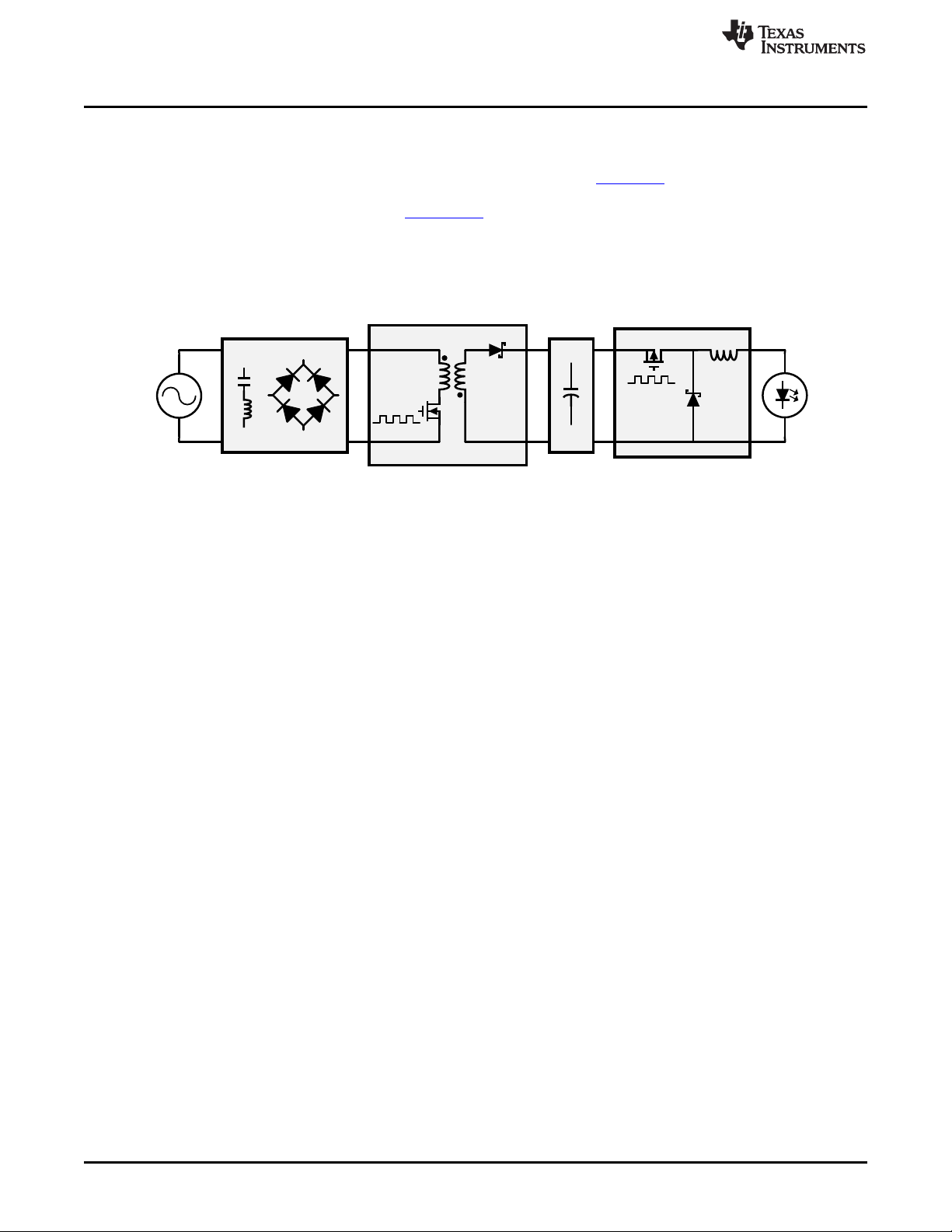
9.1 1STStage - CRM Flyback
www.ti.com
Figure 11. Two-Stage PFC LED Driver
The first stage of the evaluation board shown in Figure 11 is a critical conduction mode (CRM) flyback
converter controlled with the LM3450A. CRM converters operate at the boundary of continuous conduction
mode (CCM) and discontinuous conduction mode (DCM). CRM is implemented by turning on the main
switching FET (Q3) until the primary current rises to a peak threshold. Q3 is then turned off and the
current falls until a zero crossing is detected. At this point, Q3 is turned on and the cycle repeats.
In the CRM flyback PFC application, the rectified AC input is fed forward to the control loop, yielding a
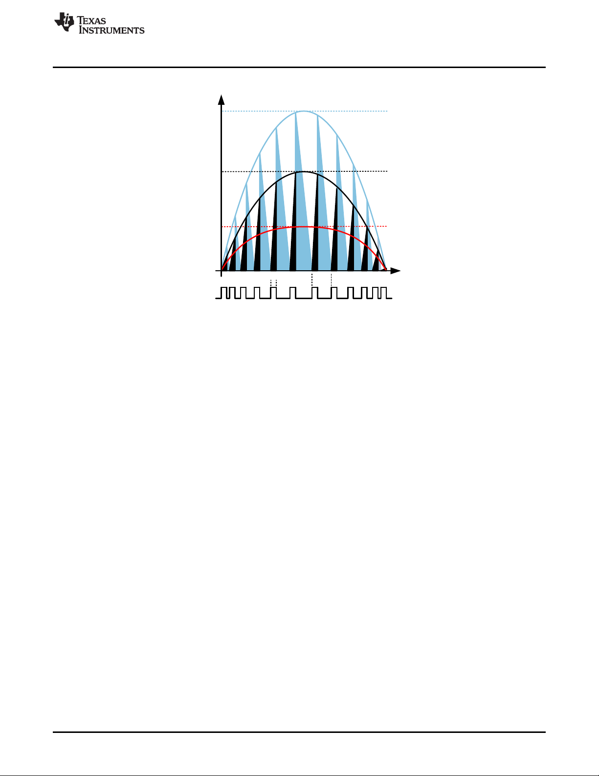
sinusoidal peak current threshold. This peak threshold creates a sinusoidal primary peak current envelope
I
as shown in Figure 12. The secondary peak current envelope I
P-pk
will simply be a scaled version of
S-pk
the primary according to the turns ratio of the transformer. Assuming good attenuation of the switching
ripple via the EMI filter, the average input current IIN(t), shown in red, can also be approximated as a
sinusoid. Since the input current has the same shape and phase as the input voltage, high power factor
(PF) can easily be achieved.
8
AN-2150 LM3450A Evaluation Board SNVA485B–June 2011–Revised May 2013
Copyright © 2011–2013, Texas Instruments Incorporated
Submit Documentation Feedback
Page 9
I
IN-PK
I
P-PK
I
S-PK
t
i
t
ON
T
SW
www.ti.com
The input current shaping happens instantly in CRM due to the feed-forward mechanism; however, the
converter must also regulate the flyback output voltage with a traditional feedback loop. This is
accomplished with a narrow bandwidth error amplifier coupled with energy storage capacitance at the
output to limit the twice line frequency ripple. The output of the error amplifier is multiplied with the scaled
rectified AC voltage to achieve both input current shaping and output voltage regulation. Refer to the
datasheet for a more detailed explanation of the power factor controller.
The LM3450A also has a phase decoder that interprets the phase dimming angle and maps it to a 500Hz
PWM open-drain output at the DIM pin. This signal is directly connected to an opto-isolator to send across
the isolation boundary to the second stage LED driver. In addition, the LM3450A provides a dynamic hold
circuit to ensure that the holding current requirement is satisfied in forward phase dimmers. Refer to the
datasheet for a more detailed explanation of the phase dimmer decoder.
Design Information
Figure 12. CRM Flyback Current Waveforms
9.2 2NDStage - Buck LED Driver
The second stage of the evaluation board is a buck LED driver controlled with the LM3409HV. The input
to this stage is the flyback output voltage and the output is a regulated constant current of 700mA to a
stack of <45V of LEDs. The LM3409HV is a hysteretic PFET controller using peak current detection and a
constant off-timer to provide regulated LED current with a constant switching frequency ripple. Coupled
with the flyback energy storage capacitance, the LM3409HV is able to remove all 120HZ ripple content
from the LED output. The 500Hz PWM signal from the first stage is used as the dimming input to the
LM3409HV. The output of the opto-isolator is connected directly to the EN pin of the LM3409HV to provide
a PWM dimmed LED current according to the detected phase angle at the primary.
The LM3409HV design is not included in this document. Refer to AN-1953 for a detialed design
procedure. The specifications for the second stage are:
• Nominal Input Voltage = 50V
• Regulated LED Current = 700mA
• Nominal LED Stack Voltage = 45V
• Switching Frequency at Nominal Input = 100kHz
• Inductor/LED Current Ripple = 115mA
9.3 CRM Flyback Converter
Operating Points
SNVA485B–June 2011–Revised May 2013 AN-2150 LM3450A Evaluation Board
Submit Documentation Feedback
Copyright © 2011–2013, Texas Instruments Incorporated
9
Page 10
Design Information
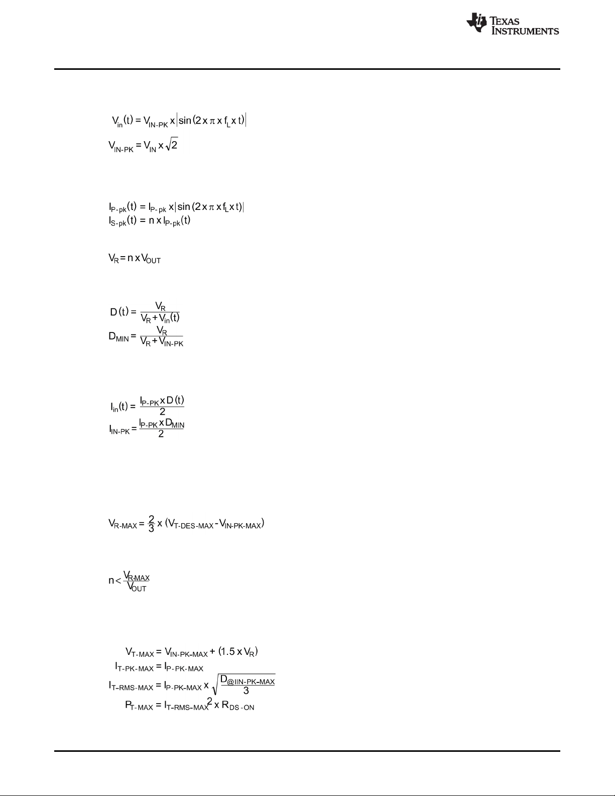
The AC mains voltage, at the line frequency fL, is assumed to be perfectly sinusoidal and the diode bridge
ideal. This yields a perfect rectified sinusoid at the input to the flyback. The input voltage Vin(t) is defined in
terms of the peak input voltage:
The controller and the transformer are also assumed to be ideal. These assumptions yield a sinusoidal
peak primary current envelope I
Both are defined in terms of the peak primary current:
The output voltage reflected to the primary is defined:
CRM control yields a variable duty cycle over a single line cycle with a minimum occurring at the peak
input voltage:
The resulting sinusoidal average input current Iin(t), shown in Figure 12, is approximated as the average of
each triangular current pulse during a switching period. The peak input current occurs at the peak primary
current:
(t) and peak secondary current envelope I
P-pk
www.ti.com
(t) as shown in Figure 12.
S-pk
(1)
(2)
(3)
(4)
Turns Ratio
The first thing to decide with an isolated design is the desired transformer turns ratio. This should be
based on the specified output voltage and the maximum peak input voltage. Frequently the MosFET is
already chosen for a design, given its cost and availability. With a desired MosFET voltage, the maximum
reflected voltage at the primary is calculated:
Generally, an integer turns ratio is selected to achieve a reflected voltage at or below the defined
maximum:
Switching MosFET
The main switching MosFET (Q3) can be sized as desired; to block the maximum drain-to-source voltage,
operate at the maximum RMS current, and dissipate the maximum power:
The peak current limit should be at least 25% higher than the maximum peak input current:
(5)
(6)
(7)
(8)
10
AN-2150 LM3450A Evaluation Board SNVA485B–June 2011–Revised May 2013
Copyright © 2011–2013, Texas Instruments Incorporated
Submit Documentation Feedback
Page 11

www.ti.com
The parallel sense resistor combination (R30||R31) has to dissipate the maximum power:
Switching Diode
The main switching diode (D10) should be sized to block the maximum reverse voltage , operate at the
maximum average current, and dissipate the maximum power:
Definitions
n – Primary to Secondary Turns Ratio
V
VIN– Nominal AC Input Voltage
V
V
I
P-PK
I
S-PK
I
IN-PK
I
LIM
D
VR– Output Voltage Reflected to Primary
V
V
V
I
T-RMS-MAX
I
T-PK-MAX
P
V
I
D-MAX
I
D-PK-MAX
P
– Regulated Output Voltage
OUT
– Peak Input Voltage
IN-PK
IN-PK-MAX
– Maximum Peak Input Voltage
– Peak Primary Current
– Peak Secondary Current
– Peak Input Current
– Peak Current Limit
– Minimum Duty Cycle over Line Cycle
MIN
– Maximum Tolerable Reflected Voltage
R-MAX
T-DES-MAX
T-MAX
– Maximum Tolerable MosFET Voltage
– Maximum MosFET Blocking Voltage
– Maximum MosFET RMS Current
– Maximum MosFET Peak Current
– Maximum MosFET Power Dissipation
T-MAX
– Maximum Diode Blocking Voltage
RD-MAX
– Maximum Diode Average Current
– Maximum Diode Peak Current
– Maximum Diode Power Dissipation
D-MAX
Design Information
(9)
(10)
(11)
9.4 Transformer
Primary Inductance
SNVA485B–June 2011–Revised May 2013 AN-2150 LM3450A Evaluation Board
Submit Documentation Feedback
Copyright © 2011–2013, Texas Instruments Incorporated
11
Page 12

Design Information
The maximum peak input current, occuring at the minimum AC voltage peak, determines the necessary
flyback transformer energy storage. As a general rule of thumb, the desired duty cycle at this worst-case
operating point should be specified near 0.5 to limit large conduction losses associated with high voltage
diodes. The maximum input current can be approximated by the maximum output power, expected
converter efficiency, and minimum input voltage. Note that there is also a 0.85 multiplier to account for the
fact that maximum power with a triac dimmer in-line is demanded at approximately 85% of the full
sinusoidal voltage waveform. Given the desired duty cycle, the maximum peak input current and
corresponding maximum peak primary current can be approximated:
Using the calculated turns ratio and the desired minimum switching frequency, the minimum necessary
primary inductance is calculated:
Switching Frequency Range
Given a primary inductance that meets the above constraint, the variable switching frequency has the
following limits:
www.ti.com
(12)
(13)
(14)
Transformer Geometries and Materials
The length of the gap necessary for energy storage in the flyback transformer can be determined
numerically; however, this can lead to non-standard designs. Instead, an appropriate ALcore value
(160nH/turns2 is a good standard value to start with) can be chosen that will imply the gap size. ALis an
industry standard used to define how much inductance, per turns squared, that a given core can provide.
With the initial chosen ALvalue, the number of turns on the primary and secondary are calculated:
(15)
Given the switching frequency range and the maximum output power, a core size can be chosen using the
vendor’s specifications and recommendations. This choice can then be validated by calculating the
maximum operating flux density given the core cross-sectional area of the chosen core.
(16)
With most common core materials, the maximum operating flux density should be set between 300mT and
3400mT. If the calculation is below this range, then ALshould be increased to the next standard value and
the turns and maximum flux density calculations iterated. If the calculation is above this range, then A
L
should be decreased to the next standard value and the turns and maximum flux density calculations
iterated.
With the flux density appropriately set, the core material for the chosen core size can be determined using
the vendor’s specifications and recommendations. Note that there are core materials that can tolerate
higher flux densities; however, they are usually more expensive and not always practical for these
designs.
12
AN-2150 LM3450A Evaluation Board SNVA485B–June 2011–Revised May 2013
Copyright © 2011–2013, Texas Instruments Incorporated
Submit Documentation Feedback
Page 13

V
OUT
V
OP1
V
OP2
Rectified AC
BIAS
LM3450A
V
CCUV
6V
14V
V
CC
VCC UVLO
C42
C44
Q1
R5
R7
Q3
V
POP2
D16
D9
D8
Q8
R18
D18
Q2
D12
R1
Q6
D11R58
C4
C5
C11
C13
D10
D23
D4
T1
R10
R11
R6
C1
www.ti.com
The rest of the transformer design should be done with the aid of the manufacturer. There are calculated
trade-offs between the different loss mechanisms and safety constraints that determine how well a
transformer performs. This is an iterative process and can ultimately result in the choice of a new core or
switching frequency range. The previous steps should reduce the number of iterations significantly but a
good transformer manufacturer is invaluable for completion of the process.
Definitions
η – Expected converter efficiency
P
V
V
I
IN-PK-MAX
I
P-PK-MAX
D
L
LP– Chosen Primary Inductance
f
SW-MIN-DES
f
SW-MIN
f
SW-MAX
NP– Number of Primary Turns
NS– Number of Secondary Turns
A
B
AL– Transformer Core Figure of Merit
OUT-MAX
IN-MIN
IN-PK-MIN
– Maximum Output Power
– Minimum RMS AC Line Voltage
– Minimum Peak Input Voltage
– Maximum Peak Input Current
– Maximum Peak Primary Current
@IIN-PK-MAX
P-MIN
– Duty Cycle at Maximum Peak Input Current
– Minimum Necessary Primary Inductance
– Desired Minimum Switching Frequency
– Minimum Switching Frequency
– Maximum Switching Frequency
– Core Cross-Sectional Area
E-MAX
– Maximum Operating Flux Density
MAX
Design Information
9.5 Bias Supplies and Capacitances
Bias Supplies
SNVA485B–June 2011–Revised May 2013 AN-2150 LM3450A Evaluation Board
Submit Documentation Feedback
Copyright © 2011–2013, Texas Instruments Incorporated
Figure 13. Bias Circuitry
13
Page 14

Design Information
The primary bias supply shown in Figure 13 enables instant turn-on through Q1 while providing an
auxiliary winding for high efficiency steady state operation. The two bias paths are each connected to V
through a diode (D8, D9) to ensure the higher of the two is providing VCCcurrent. The LM3450A BIAS pin
helps to ensure that the auxiliary winding is always providing VCCduring normal operation.
Since there is optical isolation, a secondary bias supply is also desirable. This is accomplished with
another auxiliary winding, diode (D4), and capacitance (C4, C5) which creates another flyback output that
scales with the regulated output (similar to the auxiliary primary bias winding). To ensure secondary bias
regulation is closely coupled to the regulated flyback output, the output winding is tapped to provide the
secondary bias output.
It is also advantageous to linear regulate down to approximately 9V, from the 12V bias supplies, for every
opto-isolator supply rail (V
range, preventing noise coupling into COMP and the dimming input of the LM3409.
The primary and secondary bias outputs for both versions of the board are set to 12.5V at the nominal
input voltage. The turns calculations (referred to the output) for the primary auxiliary winding and the tap
point for the secondary winding are:
The minimum primary bias supply capacitance is calculated, given a minimum VCCripple specification, to
keep VCCabove UVLO at the worst-case current:
POP1
, V
OP1
, V
) . This will stabilize the opto-isolator rail over the entire operating
OP2
www.ti.com
CC
(17)
(18)
14
AN-2150 LM3450A Evaluation Board SNVA485B–June 2011–Revised May 2013
Copyright © 2011–2013, Texas Instruments Incorporated
Submit Documentation Feedback
Page 15

+
-
5 P$
40 k:
Rectified AC
BIAS
AC
AC
LM3450A
C22
C23
R34
R36
R12
R14
R15
Q1
R5
R7
+
-
V
SEN
I
SEN
HOLD
R45
Q11
R61
D17
R44
NTC
GND
www.ti.com
Input Capacitance
The input capacitor of the flyback (C1), also called the PFC capacitor, has to be able to provide energy
during the worst-case switching period at the peak of the AC input. C1 should be a high frequency, high
stability capacitor (usually a metallized film capacitor, either polypropylene or polyester) with an AC rating
equal to the maximum input voltage. C1 should also have a DC voltage rating exceeding the maximum
peak input voltage + half of the peak to peak input voltage ripple specification. The minimum required
input capacitance is calculated given the same ripple specification:
Output Capacitance
Since the LM3450A is a power factor controller, C1 is minimized and the output capacitor (C11) serves as
the main energy storage device. C11 should be a high quality electrolytic capacitor that can tolerate the
large current pulses associated with CRM operation. The voltage rating should be at least 25% greater
than the regulated output voltage and, given the desired voltage ripple, the minimum output capacitance is
calculated:
Definitions
Δv
Δv
ΔvCC– Nominal Primary Bias Ripple
VCC– Primary Bias Capacitance
n
NA– Number of Auxiliary Turns
f2L– Twice Line Frequency
– Peak Input Voltage Switching Ripple
IN-PK
– Nominal Output Voltage Ripple
OUT
– Output to Auxiliary Turns Ratio
AUX
Design Information
(19)
(20)
SNVA485B–June 2011–Revised May 2013 AN-2150 LM3450A Evaluation Board
Submit Documentation Feedback
Figure 14. Dynamic Hold Circuit with Thermal Protection
Copyright © 2011–2013, Texas Instruments Incorporated
15
Page 16

40 45 50 55 60 65 70
0
6
12
18
24
30
36
MIN OUTPUT POWER (W)
REGULATED MIN INPUT CURRENT (mA)
120V
AC
230V
AC
Design Information
9.6 Hold Current
Dynamic Hold
The LM3450A regulates the minimum input current with a dynamic hold circuit to ensure the triac holding
current requirement is satisfied. The regulated minimum current is set by choosing the sense resistor
(R34||R36):
The maximum possible holding current (usually occurs during transients when triac fires) is set by
choosing the hold resistor (R12||R14||R15) between the source of the Q1 and HOLD:
PassFET
The passFET (Q1) is used in its linear region to stand-off the line voltage from the LM3450A controller.
Both the VCCstartup current and the triac holding current are conducted through the device. Since the
holding current is far larger than the startup current and is dynamically adjusted every cycle, it will
dominate the calculations. Given this, Q1 is chosen to block the maximum peak input voltage and conduct
the maximum holding current. The surge handling capability of Q1 is also important and is evaluated by
looking at the safe operating area (SOA) of the device.
Finally, Q1 needs to be able to dissipate the maximum power. Looking at an absolute worst-case
condition for the Q1 (during open load where the converter draws near-zero power), extremely large
power dissipation is required (many Watts). Designing for this case is unrealistic and costly. Instead,
Figure 15 can be used to find the maximum I
minimum output power is defined as the output power that causes the dynamic hold to force
approximately 1W of power dissipation in Q1 (causing approximately 100°C rise in a DPAK). Below the
minimum output power level, Q1 can reach temperatures exceeding 125°C, depending on the conduction
angle, causing potential catastrophic failure. Figure 15 is only a general guideline based on experimental
testing of this evaluation board. Each application will have a different passFET thermal characteristic,
which suggests thermal protection of the passFET is usually necessary.
IN-MIN-REG
www.ti.com
(21)
(22)
for the desired minimum output power level. The
16
AN-2150 LM3450A Evaluation Board SNVA485B–June 2011–Revised May 2013
Figure 15. Output Power Restrictions
(without thermal protection)
Copyright © 2011–2013, Texas Instruments Incorporated
Submit Documentation Feedback
Page 17

+
-
DIM
V
AC
500k
Transition
LM3450A
OPTO2
V
POP2
Rectified AC
ANGLE
DEMOD
SAMPLE/REMAP
D
IN
D
OUT
D
IN
D
OUT
R25 R24
C18 C17
R16
R71
R26
R29
R32
FLT2
FLT1
V
ADJ
V
REF
3V
REF
R23
D22
500 Hz
U8
V
OP2
LM3409HV
EN
www.ti.com
Thermal Protection
Using the previously mentioned design methodology, thermal protection is indeed necessary for the open
load condition and for power levels below the specified operating range shown in Figure 15. The thermal
protection circuit shown in Figure 14 will reduce the maximum holding current when the temperature rises
too high, thus preventing catastrophic failure of Q1. Keep in mind that the thermal foldback does not
prevent the circuit from operating, it simply reduces the amplitude of the dynamic hold. The only negative
effect of the thermal protection is a possible reduction in contrast ratio, meaning the minimum attainable
output current potentially increases as the dynamic hold level decreases.
The thermal protection is accomplished using a PNP transistor (Q11) and a resistor divider comprised of a
fixed resistor (R45) and an NTC thermistor (R44). As Q1 heats up, R44 decreases causing the collector
voltage of Q11 to decrease, effectively reducing the maximum attainable holding current. Placement of
R44 is critical to ensure the best possible thermal coupling to Q1. The drain of Q1 will have the highest
temperature rise but it is at a much higher voltage than the source where R44 is electrically connected.
Because of this, the best placement for R44 is on the other side of the PCB, directly under the drain of
Q1. The dielectric of the PCB provides adequate electrical insulation while yielding the best thermal
coupling. Obviously, R44 placement in potted solutions is much more forgiving. A 10kΩ NTC is suggested
for R44 and Q11 can be a basic PNP (i.e. MMBT3906). R45 has to be sized experimentally since the
thermal coupling will vary with each PCB layout. A good starting point for R45 is 15kΩ.
Definitions
I
IN-MIN-REG
I
HOLD-MAX
Design Information
– Regulated Minimum Input Current
– Maximum Hold Current
9.7 Dimming Decoder
SNVA485B–June 2011–Revised May 2013 AN-2150 LM3450A Evaluation Board
Submit Documentation Feedback
Figure 16. Dimming Decoder Circuit
. A general rule of thumb is to set V
DET
Angle Sense
VACis a dual input for both the PFC multiplier and the angle decoder. The resistor divider (R26+R29, R32)
should be sized according to the desired angle detect voltage V
V
/x where x is a value between 4 and 7. R26+R29 should be chosen to be between 1MΩ and 2MΩ to
IN-PK
limit power dissipation.
Copyright © 2011–2013, Texas Instruments Incorporated
DET
=
(23)
17
Page 18

0.0 0.2 0.4 0.6 0.8 1.0
0.0
0.2
0.4
0.6
0.8
1.0
1.2
LM3409HV EN PIN DUTY CYCLE
LM3450A DEMODULATED VAC PIN DUTY CYCLE
1V
0.5V
2V
2.5V
1.5V
V
ADJ
=3V
Design Information
Decoder Mapping
The mapping from the demodulated input (VAC pin of the LM3450A) to output (EN pin of the LM3409HV)
is shown in Figure 17. Varying V
mind that the demodulated input angle is a function of the resistor divider at the VACpin. This means that
the input duty cycle can be shifted by changing V
Filters
The filters (FLT1, FLT2) are chosen to provide the desired dimming transition response (how the light
changes during dimmer movement). The filter frequency should be set between 2Hz and 10Hz for best
operation (2Hz has a fade feeling, 10Hz is very snappy). The capacitors (C17, C18) can both be set to
1µF for all designs and given the filter frequencies, the resistors (R24, R25) are calculated:
will adjust the mapping as desired for the target dimmers. Keep in
ADJ
within the previously suggested range.
DET
www.ti.com
(24)
Opto-Isolator
A standard low cost opto-isolator (same type used for feedback of the output) is used to transfer the
dimming command from DIM to the secondary. It needs to be driven with at least 1-2mA of current to
obtain full 70:1 contrast ratio (more current creates faster edges). With V
there is > 1mA of drive current. The output of the opto-isolator should be clamped to just above the
dimming input threshold of the secondary driver. This is accomplished with a 1.8V Zener clamp (D22) at
the EN pin of the LM3409HV on the evaluation boards. R71 needs to be large enough that the Zener
clamp is activated whenever the LM3409HV EN pin should be high.
Definitions
V
– Rectified AC Angle Detect Voltage
DET
f
18
– FLT1 frequency
FLT1
f
– FLT2 frequency
FLT2
AN-2150 LM3450A Evaluation Board SNVA485B–June 2011–Revised May 2013
Figure 17. Dimming Decoder Mapping
Copyright © 2011–2013, Texas Instruments Incorporated
= 9V and R16 = 6.04kΩ,
POP2
Submit Documentation Feedback
Page 19

OPTO GAINS & EXTERNAL
ERROR AMPLIFIER
FLYBACK POWER STAGE
FEEDBACK GAIN
+
-
LM3450A MULTIPLIER &
SENSING GAINS
V
REF
V
OUT
V
COMP
V
FB
I
CONT
V
E
+
-
G
COMP
G
3450
G
VC
H
FB
www.ti.com
9.8 Voltage Control Loop
The CRM topology requires a narrow bandwidth voltage control loop to regulate the output voltage. This
loop needs to be compensated to maintain stability over the desired operating range. The flyback topology
is isolated, therefore the LM3450A internal error amplifier is bypassed and an external secondary side
error amplifier is used instead. The control loop shown in Figure 18 is comprised of the converter controlto-output transfer function, the compensator transfer function, and all of the other gains in the loop.
The output voltage is sensed with a resistor divider (R81, R72) and regulated to 1.24V using an LMV431:
Design Information
Figure 18. Control Loop Block Diagram
(25)
The converter control-to-output transfer function can be approximated as a single pole system:
(26)
The feedback gain (HFB) is unity due to the control implementation and the LM3450A device and external
gains are defined:
(27)
A standard PI compensator is used on the secondary to stabilize the system. The error amplifier is
implemented with an LMV431 and a series resistor (R77) and capacitor (C35) in the feedback path as
shown in Figure 19. The output of the LMV431 is tied to the cathode of the opto photo-diode. A resistor
(R70 = 2kΩ) from the anode of the photodiode to the bias rail provides the current path and ultimately the
output voltage swing of the secondary error amplifier. The primary side of the opto is connected directly to
COMP. With the 5kΩ internal pull-up resistor, the maximum current through the primary side of the opto
will be 1mA. A higher frequency roll-off pole is placed on the primary in the form of a capacitor (C24) from
COMP to GND. The resistor divided flyback output voltage is regulated to the 1.24V LMV431 internal
reference. Note the additional soft-start circuit using C34, D13, and D14.
SNVA485B–June 2011–Revised May 2013 AN-2150 LM3450A Evaluation Board
Submit Documentation Feedback
Copyright © 2011–2013, Texas Instruments Incorporated
19
Page 20

V
OUT
V
OP1
LMV431
COMP
OPTO
5V
LM3450A
5k
R72
R81
R77
C35
R70
C24
SOFT
START
FB
R38
U10
U9
D13
D14
C34
Design Information
The compensator transfer function is defined:
www.ti.com
Figure 19. Secondary Error Amplifier Circuit
(28)
Where the secondary compensator pole is defined:
(29)
And the compensator zero is defined:
(30)
And the primary roll-off pole is defined:
(31)
The resulting control loop gain is
(32)
The compensator design for this system can be complicated; however with some useful assumptions, it
can be simplified. Looking at the total DC gain (G
3450xGC0xHFB
), the following can be made relatively
constant over all designs:
• R70 = 2kΩ, the 5kΩ internal pull-up, and the 0.55 multiplier gain.
• The opto CTR, though variable over temperature, given a fixed supply rail and a fixed R70 value.
In several cases, the product of two DC gain terms can also be identified as relatively constant over all
designs if all of the previous LM3450A design methodology is observed:
20
• V
• I
Given these relationships and following the complete LM3450A design method, the DC gain should only
vary largely with change in output voltage (directly proportional).
The output pole of the converter on the other hand follows these basic relationships:
AN-2150 LM3450A Evaluation Board SNVA485B–June 2011–Revised May 2013
and KVare almost exactly inversely proportional (given x remains constant when solving V
INPK
VIN/x).
P-PK
I
P-PK
and R30||R31 are closely inversely proportional (given current limit is a constant percentage above
).
Copyright © 2011–2013, Texas Instruments Incorporated
Submit Documentation Feedback
DET
=
Page 21

D21
D24
R20
C12
R21
COMP
LM3450A
BIAS
V
ADJVCC
Q4
D20
www.ti.com
Design Information
• P
OUT-MAX
there is no relative change to ωP1.
• V
is exactly inversely proportional to ωP1given a constant output ripple specification.
OUT
With the opposing conditions of the output pole moving inversely proportional to V
moving proportional to V
this, the exact compensator on this evaluation board can be a starting point for any LM3450A design.
During prototyping, If stability becomes a concern, the R77 value can be changed to improve stability. In
general the compensator calculated in the Design Calculations section is sized to be stable and have a
bandwidth of around 50-60Hz. This is a fairly high bandwidth for a PFC converter which will cause there to
be some 120Hz ripple on COMP. This will decrease PF but improve transient response which is very
helpful in phase dimmable applications.
Since it is usually desirable to maximize bandwidth (within the PFC limitation), there is a simple method to
adjust the R77 value. Measure the twice-line frequency ripple on COMP. If the ripple is less than 200300mV, increase R77 until it is within that range. If the ripple is larger, then decrease R77 until it is within
that range. This will result in a very small PFC degradation, while maximizing bandwidth of the control
loop.
9.9 STARTUP
When using the LM3450A with a phase dimmer, startup can be very disruptive. Any time the dimmer is
turned on (via a separate switch or some state where the dimmer has been previously disconnected from
its load), the LM3450A will attempt to bring the system to regulation. Because phase dimmers can be
turned on and off quickly, the system capacitances may or may not be fully discharged, this can lead to a
large variance in startup conditions. The best way to control startup transients is to softstart the dimming
command and the PFC control simultaneously. This can be accomplished with the circuit shown in
Figure 20. D20 is a dual common cathode schottky with very low forward voltage to allow COMP and
VADJ to be pulled as close to zero as possible. The softstart time constant is set by C12 and R20. Q4,
R21, and D21 form a reset circuit for C12. Since BIAS transitions to 20V whenever VCC hits the falling
UVLO threshold and D21 is an 18V Zener, the base of Q4 will go high turning on Q4 and immediately
resetting the capacitor to 0V. Then when VCC reaches the UVLO rising threshold and BIAS transitions to
14V, Q4 turns off and softstart is active again.
and C11 are exactly directly proportional given a constant output ripple specification, therefore
and the DC gain
, the net result gives a very consistent uncompensated loop gain. Because of
OUT
OUT
Figure 20. Primary Soft-start Circuit
Relevant Definitions
GVC(s) – Converter Control-to-Output Transfer Function
GC0– Converter Control-to-Output DC Gain
G
– LM3450A and External Gains
3450
G
(s) – Compensator Transfer Function
COMP
HFB– Feedback Gain
ω
– Converter Output Pole
P1
ω
– Compensator Secondary Integrator Pole
P2
Copyright © 2011–2013, Texas Instruments Incorporated
SNVA485B–June 2011–Revised May 2013 AN-2150 LM3450A Evaluation Board
Submit Documentation Feedback
21
Page 22

RET
VREF
+
-
AC
RET
To VAC divider and passFET
LED
Driver
+
-
Y-cap across Xformer
C7
C1
C8
C9
C30
R8
R9
R56
L4
L1
R57
R39
R48
R62
R34
R36
C26
L2
C2
C3
C66
R2
R3
R47
D25
R51
Design Information
9.10 Input Filter
22
www.ti.com
ω
– Compensator Secondary Zero
Z1
ω
– Compensator Primary HF Pole
P3
T(s) – Total Loop Gain
Figure 21. Input EMI Filter
Background
Since the LM3450A is used for AC to DC systems, electromagnetic interference (EMI) filtering is critical to
pass the necessary standards for both conducted and radiated EMI. This filter will vary depending on the
output power, the switching frequencies, and the layout of the PCB. There are two major components to
EMI: differential noise and common-mode noise. Differential noise is typically represented in the EMI
spectrum below approximately 500kHz while common-mode noise shows up at higher frequencies.
Conducted
Figure 21 shows a typical filter used with an LM3450A design. To conform to conducted standards, a
fourth order filter (two second order stages) is implemented using shielded inductors (L1, L2, L4), an EMI
suppression X1/X2 film capacitor (C7), and a pulse-rated film capacitor (C1) which is also the primary PFC
capacitor sized previously. In addition to the basic filter components, damping is used to prevent excitation
of the resonant frequencies of the filter itself. The best practice for damping an EMI filter is to use an RC
damper network across each filter capacitor. The C of the damper should be set to be 3 times the filter
capacitor value. This EMI filter, if sized properly, can provide ample attenuation of the switching frequency
and lower order harmonics contributing to differential noise. The filter can be described as follows:
• Stage 1 pole: L1+L4 and C7 gives 40db/decade roll-off
– Stage 1 damping: C8||C9||C30 and R8||R9||R56
• Stage 2 pole: L2 and C1 gives 40db/decade roll-off
– Stage 2 damping: C2||C3||C66 and R2||R3||R47
Since L1 and L4 are symmetrically placed in both the line and neutral legs of the AC line, they help to
reduce common-mode noise also. It is sometimes necessary to place a high value resistance (R48, R51,
R62) across each inductor to prevent excitation of the SRF of the inductor which is usually at higher
frequencies. A Y1/Y2 film capacitor (C26) from the primary ground to the secondary ground is also
commonly used for reduction of common mode noise.
Radiated
Conforming to radiated EMI standards is much more difficult and is dependent on the entire system
including the enclosure. C26 will greatly help reduce radiated EMI; however, reduction of dV/dt on
switching edges and PCB layout iterations are frequently necessary as well. Consult available literature
and/or an EMI specialist for help with this. It can be a daunting task.
AN-2150 LM3450A Evaluation Board SNVA485B–June 2011–Revised May 2013
Copyright © 2011–2013, Texas Instruments Incorporated
Submit Documentation Feedback
Page 23

t
V
SW
V
RING
V
R
V
IN
ZCD
V
IN
V
OUT
TVS
D1
D5
Q3
D10
D23
C11
C13
T1
www.ti.com
Interaction with Dimmers
In general, input filters and forward phase dimmers do not work well together. The triac needs a minimum
amount of holding current to function. The converter itself is demanding a certain amount of current from
the input to provide to its output. With no filter, the difference of the necessary hold current and the
converter current is provided by the LM3450A dynamic hold circuit. Unfortunately, the actual dimmer
current is not being monitored; instead a filtered version is being measured. In reality, the input filter is
providing or taking current depending upon the dV/dt of the capacitors. The discrepancy between the
measured input current at ISEN and the actual input current through the triac is the worst at the highest
dV/dt of the input filter capacitors. The best way to deal with this problem is to minimize filter capacitance
and increase the regulated hold current until there is enough current to satisfy the dimmer and filter
simultaneously.
Figure 21 shows one effective way to improve the dynamic hold functionality when using an EMI filter. The
hold current path through the passFET is derived between the two filter stages. In this configuration, the
measured input current has only one stage of filtering capacitance to contribute to the descrepancy
between measured and actual input current. In addition, the damping network for the C7 capacitor is
directly connected to the dynamic hold point of the rectified AC (passFET drain). This, combined with the
filter stage between the passFET and the transformer, help attenuate any unwanted switching frequency
coupling into the dynamic hold circuit.
This configuration also provides some extra filtering of the feedforward VAC signal, which is now derived
at the same point as the dynamic hold. One important addition to this EMI filter is a back-to-back TVS
clamp across L2. During transient conditions, if the L2 filter rings too much, the current will try to change
directions. There is no continuous path for current at the passFET drain, therefore the voltage can rise
uncontrolled and damage the passFET. A 20V back-to-back TVS is sufficient to provide this protection.
Design Information
9.11 Inrush Limiting, Damping and Clamping
Clamp
In any flyback converter there exists large ringing (V
due to the rising edge of the Q3 drain after turn-off, which excites the resonance created by the leakage
inductance of the transformer and output capacitance of Q3. A clamp circuit is necessary to prevent
damage to Q3 from excessive voltage. The evaluation boards use a transil (TVS) clamp, shown in
Figure 23
When Q3 is on and the drain voltage is low, the blocking diode (D5) is reverse biased and the clamp is
inactive. When the MosFET is turned off, the drain voltage rises past the nominal voltage (reflected
voltage plus the input voltage). If it reaches the TVS clamp voltage + the input voltage, the clamp prevents
any further rise. The TVS diode (D1) voltage is set to prevent the MosFET from exceeding its maximum
rating:
Figure 22. Switch Node Ringing Figure 23. Transil Clamp
) on the Q3 drain, as shown in Figure 22. This is
RING
SNVA485B–June 2011–Revised May 2013 AN-2150 LM3450A Evaluation Board
Submit Documentation Feedback
Copyright © 2011–2013, Texas Instruments Incorporated
23
Page 24

t
Iin(t)
0
Potential Misfire
Triac Fires Æ Inrush Spike
Design Calculations - 120V, 30W
This clamp method is fairly efficient and very simple compared to other commonly used methods. Note
that if the ringing is large enough that the clamp activates, the ringing energy is radiated at higher
frequencies. Depending on PCB layout, EMI filtering method, and other application specific items, the
transil clamp can present problems conforming to radiated EMI standards.
If the transil clamp becomes problematic at higher frequencies, an RCD clamp can be used to dampen the
ringing. Looking at the EMI Performance section, it is obvious that the evaluation board fails near 30MHz.
This would indicate an RCD clamp is indeed necessary for this design. C29 and R49, shown on the
Complete Evaluation Board Schematic can be populated as desired to improve the EMI signature. This
will degrade efficiency some.
Inrush
With a forward phase dimmer, a very steep rising edge causes a large inrush current every cycle as
shown in Figure 24. Series resistance (R39, R57) can be placed between the filter and the triac to limit the
effect of this current on the converter. This will, of course, degrade efficiency but some inrush protection is
also necessary in any AC system due to startup. The size of R39 and R57 are best found experimentally
as they provide attenuation for the whole system.
The inrush spike excites resonance(s) of the input filter, which can cause the current to ring negative, as
shown in Figure 24, thereby shutting off the triac. The RC damper of the first stage of the input filter
should be increased to dampen the worst-case ringing energy due to this edge. This can require a
significant increase in capacitance depending upon the dimmer tested (more than 10x the filter
capacitance). The resistance is then experimentally changed to create a ringing waveform that is most
contained. The objective is to prevent the input current ringing from crossing the minimum regulated
holding current thereby preventing misfires.
www.ti.com
(33)
Figure 24. Inrush Current Spike
10 Design Calculations - 120V, 30W
The following is a step-by-step procedure with calculations for the 120V 30W Evaluation Board. The 230V
calculations can be done in the same manner. Many components are identical between both boards for
simplicity, therefore some components on the 120V board are over-sized.
10.1 Specifications
24
fL– 60Hz
AN-2150 LM3450A Evaluation Board SNVA485B–June 2011–Revised May 2013
Copyright © 2011–2013, Texas Instruments Incorporated
Submit Documentation Feedback
Page 25

www.ti.com
f
– 45kHz
SW-MIN
VIN– 120V
V
IN-MIN
V
IN-MAX
I
– 700mA
LED
Δv
OUT
Δv
IN-PK
I
P-PK-LIM
V
T-DES-MAX
P
OUT-MAX
D
@IIN-MAX-PK
V
OUT
– 90V
– 135V
= 2V
= 60V
= 3A
= 30W
= 50V
AC
AC
AC
= 400V
= 0.5
η=0.9
10.2 Preliminary Calculations
Maximum peak input voltage:
Minimum peak input voltage:
Design Calculations - 120V, 30W
(34)
Maximum average input current:
Maximum peak input current:
Maximum peak primary current:
10.3 Main Switching MOSFET
Maximum drain-to-source voltage:
Maximum peak MosFET current:
Maximum RMS MosFET current:
Maximum power dissipation:
(35)
(36)
(37)
(38)
(39)
(40)
(41)
Resulting component choice:
SNVA485B–June 2011–Revised May 2013 AN-2150 LM3450A Evaluation Board
Submit Documentation Feedback
Copyright © 2011–2013, Texas Instruments Incorporated
(42)
25
Page 26

Design Calculations - 120V, 30W
10.4 Re-Circulating DIODE
Maximum reverse blocking voltage:
Maximum peak diode current:
Maximum average diode current:
Maximum power dissipation:
Resulting component choice:
10.5 Current Sense
Sense resistor:
www.ti.com
(43)
(44)
(45)
(46)
(47)
(48)
Power dissipation:
Resulting component choice:
10.6 Input Capacitance
Minimum capacitance:
Voltage rating:
Resulting component choice:
10.7 Output Capacitance
Minimum capacitance:
(49)
(50)
(51)
(52)
(53)
(54)
26
(55)
Voltage rating:
(56)
Resulting component choice:
AN-2150 LM3450A Evaluation Board SNVA485B–June 2011–Revised May 2013
Copyright © 2011–2013, Texas Instruments Incorporated
Submit Documentation Feedback
Page 27

www.ti.com
10.8 Transformer
Maximum acceptable reflected voltage:
Primary to secondary turns ratio:
Actual reflected voltage:
Primary to auxiliary turns ratio:
Transformer primary inductance:
Number of primary turns:
Design Calculations - 120V, 30W
(57)
(58)
(59)
(60)
(61)
(62)
Number of secondary turns:
Number of auxiliary turns:
Maximum flux density:
Resulting component choice:
10.9 Transil Clamp
TVS clamp voltage:
Resulting component choice:
(63)
(64)
(65)
(66)
(67)
(68)
SNVA485B–June 2011–Revised May 2013 AN-2150 LM3450A Evaluation Board
Submit Documentation Feedback
Copyright © 2011–2013, Texas Instruments Incorporated
(69)
27
Page 28

:o
:o
+
k1032R
M129R26R
Design Calculations - 120V, 30W
10.10 Dynamic Hold
ISEN sense resistance:
HOLD resistance:
Resulting component choice:
10.11 Decoder Input
Resistor divider:
Resulting component choice:
www.ti.com
(70)
(71)
(72)
(73)
(74)
10.12 Output Voltage Sense
Resistance:
Resulting component choice:
10.13 Loop Compensation
Converter output pole:
Converter DC gain:
LM3450A and external sensing DC gain:
Secondary compensator dominant pole:
(75)
(76)
(77)
(78)
(79)
(80)
Secondary compensator zero:
(81)
28
AN-2150 LM3450A Evaluation Board SNVA485B–June 2011–Revised May 2013
Copyright © 2011–2013, Texas Instruments Incorporated
Submit Documentation Feedback
Page 29

:o
Po
Po
k30.177R
F124C
F1035C
www.ti.com
Primary roll-off pole:
Resulting component choice:
Design Calculations - 120V, 30W
(82)
(83)
SNVA485B–June 2011–Revised May 2013 AN-2150 LM3450A Evaluation Board
Submit Documentation Feedback
Copyright © 2011–2013, Texas Instruments Incorporated
29
Page 30

Q3
R28
R31
R32
R29
R30
Q1
R5
R7
Flyback PFC
C2
C3
VDC
SBIAS
C11
C5
R2
D1
R26
R6
R11
R3
L1
L4
C9
C30
R9
R56
R10
C21
V+
R23
R27
VREF
1
COMP
7
VAC
6
VADJ2FLT2
3
CS
11
FB
8
ZCD14VCC
13
ISEN
9
GATE
12
GND
10
DIM5FLT1
4
HOLD
15
BIAS
16
U1
C23
DIM
R24
C17
C22
R12R14
D10
C13
C4
9
8
2
1
3
.
5
4
.
7
6.
.
10
3010
40
40
T1
D5
C44
D8
D4
D9
C18
R25
C20
R33
F1
C7
D2
D3
D6
D7
C1
R36
RETURN
C43
C46
PBIAS
J1
R15
R34D17
D16
J3
C14
R21
R38
C24
R55
C26
C42
C31
C40
UVLO
1
CSN
7
PGATE
6
IADJ
2
EN
3
CSP
8
VCC
9
VIN
10
GND
5
COFF
4
U11
R84
D15
L3
EN
C38
R78
R83
R75
R73
C39
C36
Q7
VOUT
C10
R4
R13
EN
C37
C47
VDC
VOUT
R19
SDIM
Buck LED Driver
R1
Q2
D12
Sbias
O1bias
R58
Q6
D11
Sbias
O2bias
U10
R70
R77
R81
R72
C34
C35
1
2
5
436
U9
D14
1
2
5
436
U8
R71
SDIM
R69
DIM
R16
O1Pbias
R41
R43
R40
PBIAS
R42
COMP
FB
C25
VDC
O1bias
O2bias
Linear Regulators
Input Filter
Dimming
Compensation
Softstart
Q11
R45
R44
R17
D21
D13B
D13A
RETURN
J12
J10
J8
J14
J13
R48
R62
R49
C29
R22
BIAS
D22
R57
R39
R20
D20
C12
R59
R60
C28
R54
D23
EP
R18
Q8
D18
Pbias
O1Pbias
PBIAS
COMP
FB
V+
Q2
Q2
Q2
R66
R65
SGND
R46
R47
C66
PGND
VADJ
C8
R8
LINE
LED+
VADJ COMP PBIAS
BIAS
ZCD
ZCD
RETURN
R63
R64
L2
R51
D24
D25
J2
LED-
NEUT
Q20
R61
VR1
Complete Evaluation Board Schematic
www.ti.com
11 Complete Evaluation Board Schematic
30
AN-2150 LM3450A Evaluation Board SNVA485B–June 2011–Revised May 2013
Figure 25. Complete Evaluation Board Schematic
Copyright © 2011–2013, Texas Instruments Incorporated
Submit Documentation Feedback
Page 31

www.ti.com
12 120V Bill of Materials
Reference Designator Part Value Manufacturer Part Number
C1 CAP MPY 0.22µF 400V RAD WIMA MKP10-.22/400/20
C2, C3, C8, C9, C30, C66 CAP CER 0.22µF 250V RAD TDK FK20X7R2E224K
C4, C44 CAP ELEC 220µF 35V RAD NICHICON UHE1V221MPD
C5, C23, C42, C46 CAP CER 0.10µF 25V 0603 MURATA GRM188R71E104KA01D
C7 CAP MPY 33nF 330VAC X1 RAD EPCOS B32912A3333M
C11 CAP ELEC 1000µF 63V RAD NICHICON UPW1J102MHD6
C12 CAP CER 47µF 6.3V 1206 MURATA GRM31CR60J476ME19L
C13, C34, C47 CAP CER 1µF 100V 1206 TDK C3216X7R2A105M
C17, C18, C24, C36 CAP CER 1µF 16V 0603 MURATA GRM188R71C105KA12D
C21, C43 CAP CER 10nF 25V 0603 MURATA GRM188R71E103KA01D
C22 CAP CER 0.22µF 16V 0603 TDK C1608X7R1C224K
C26 CAP CER 4.7nF 500VAC Y1 RAD EPCOS VY1472M63Y5UQ63V0
C35 CAP CER 10µF 16V 1206 MURATA GRM31CR71C106KAC7L
C37 CAP CER 0.10µF 50V 0603 MURATA GRM188R71H104KA93D
C38 CAP CER 2.2µF 6.3V 0603 TDK C1608X5R0J225M
C39 CAP CER 470pF 100V 0603 TDK C1608C0G2A471J
D1 DIODE TVS 150V 600W UNI SMB LITTLEFUSE SMBJ150A
D2, D3, D6, D7 DIODE GEN PURPOSE 1000V 1A SMA COMCHIP CGRA4007-G
D4, D9 DIODE ULTRAFAST 100V 0.2A SOT-23 FAIRCHILD MMBD914
D5 DIODE ULTRAFAST 600V 1A SMA FAIRCHILD ES1J
D8, D10, D23 DIODE ULTRAFAST 200V 1A SMA FAIRCHILD ES1D
D11, D12, D18 DIODE ZENER 10V 500mW SOD-123 FAIRCHILD MMSZ5240B
D13 DIODE ULTRAFAST 70V 0.2A SOT-23 FAIRCHILD BAV99
D14 DIODE ZENER 3.3V 500mW SOD-123 ON-SEMI MMSZ3V3T1G
D15 DIODE SCHOTTKY 60V 2A SMB ON-SEMI SS26T3G
D16 DIODE ZENER 24V 1.5W SMA MICRO-SEMI SMAJ5934B-TP
D17 DIODE SCHOTTKY 50V 3A SMA FAIRCHILD ES2AA-13-F
D20 DIODE SCHOTTKY (DUAL) 30V 0.5A SOT-23 DIODES INC PMEG3005CT,215
D21 DIODE ZENER 18V 500MW SOD-123 FAIRCHILD MMSZ5248B
D22 DIODE ZENER 1.8V 500MW SOD-123 ON-SEMI MMSZ4678T1G
D24 DIODE ZENER 3.9V 500MW SOD-123 ON-SEMI MMSZ4686T1G
D25 DIODE TVS 20V 400W BIDIR SMA LITTLEFUSE SMAJ20CA
F1 FUSE 500mA T-LAG RST BEL FUSE RST 500
J1, J2 CONN HEADER 2x1 VERT AMP 1-1318301-2
L1, L2, L4 IND SHIELD 1mH 1.14A SMT COILCRAFT MSS1278-105KL
L3 IND SHIELD 270µH 2.18A SMT COILCRAFT MSS1278-274KL
Q1 MOSFET N-CH 800V 3A DPAK ST MICRO STD4NK80ZT4
Q2, Q6, Q8 TRANS NPN 40V 0.6A SOT-23 FAIRCHILD MMBT4401
Q3 MOSFET N-CH 500V 9A DPAK ST MICRO STD11NM50N
Q4 TRANS NPN 40V 0.2A SOT-23 FAIRCHILD MMBT3904
Q7 MOSFET P-CH 70V 5.7A DPAK ZETEX ZXMP7A17K
Q11 TRANS PNP 40V 0.2A SOT-23 FAIRCHILD MMBT3906
R1, R18, R32, R58 RES 10kΩ 1% 0.1W 0603 VISHAY CRCW060310K0FKEA
R2, R3, R8, R9, R47, R56 RES 820Ω 5% 1W 2512 VISHAY CRCW2512820RJNEG
R5, R7 RES 200kΩ 1% 0.25W 1206 VISHAY CRCW1206200KFKEA
R6, R11 RES 10Ω 1% 0.25W 1206 VISHAY CRCW120610R0FKEA
120V Bill of Materials
Table 1. 120V Bill of Materials
SNVA485B–June 2011–Revised May 2013 AN-2150 LM3450A Evaluation Board
Submit Documentation Feedback
Copyright © 2011–2013, Texas Instruments Incorporated
31
Page 32

120V Bill of Materials
R10 RES 40.2Ω 1% 0.25W 1206 VISHAY CRCW120640R2FKEA
R12, R14, R15 RES 301Ω 1% 0.25W 1206 VISHAY CRCW1206301RFKEA
R16 RES 6.04kΩ 1% 0.125W 0805 VISHAY CRCW08056K04FKEA
R17 RES 100kΩ 1% 0.1W 0603 VISHAY CRCW0603100KFKEA
R19, R41, R43, R61, R73 RES 0Ω 5% 0.1W 0603 VISHAY CRCW06030000Z0EA
R20 RES 499kΩ 1% 0.1W 0603 VISHAY CRCW0603499KFKEA
R21, R69 RES 20.0kΩ 1% 0.1W 0603 VISHAY CRCW060320K0FKEA
R23 RES 6.04kΩ 1% 0.1W 0603 VISHAY CRCW06036K04FKEA
R24, R25 RES 75.0kΩ 1% 0.1W 0603 VISHAY CRCW060375K0FKEA
R26, R29 RES 499kΩ 1% 0.25W 1206 VISHAY CRCW1206499KFKEA
R28 RES 10Ω 1% 0.125W 0805 VISHAY CRCW080510R0FKEA
R30, R31, R65, R66, R83 RES 1.00Ω 1% 0.25W 1206 VISHAY CRCW12061R00FKEA
R34, R36 RES 5.62Ω 1% 0.25W 1206 VISHAY CRCW12065R62FKEA
R38 RES 5.11kΩ 1% 0.1W 0603 VISHAY CRCW06035K11FKEA
R39, R57 RES 5Ω 1% 3W WIREWOUND VISHAY PAC300005008FAC000
R44 THERM 10kΩ NTC 0603 MURATA NTCG163JF103F
R45 RES 15.0kΩ 1% 0.1W 0603 VISHAY CRCW060315K0FKEA
R46 RES 5.11kΩ 1% 0.125W 0805 VISHAY CRCW08055K11FKEA
R48, R51, R62 RES 20.0kΩ 1% 0.25W 1206 VISHAY CRCW120620K0FKEA
R55 RES 51.1kΩ 1% 0.25W 1206 VISHAY CRCW120651K1FKEA
R70 RES 2.00kΩ 1% 0.125W 0805 VISHAY CRCW08052K00FKEA
R71 RES 10.0kΩ 1% 0.125W 0805 VISHAY CRCW080510K0FKEA
R72 RES 105kΩ 1% 0.125W 0805 VISHAY CRCW0805105KFKEA
R77 RES 30.1kΩ 1% 0.1W 0603 VISHAY CRCW060330K1FKEA
R81 RES 2.67kΩ 1% 0.1W 0603 VISHAY CRCW06032K67FKEA
R84 RES 49.9kΩ 1% 0.1W 0603 VISHAY CRCW060349K9FKEA
T1 XFORMER 120V 30W OUTPUT 50V WURTH 750813651
U1 IC PFC CONT 16-TSSOP TI LM3450
U8, U9 OPTO-ISOLATOR SMD LITE ON CNY17F-3S
U10 IC SHUNT REG SOT-23 NSC LMV431AIM5
U11 IC LED DRIVR 10-eMSOP NSC LM3409HVMY
C10, C14, C20, C25, C28, Did not populate
C29, C31, C40, Q20, R4,
R13, R22, R27, R33, R40,
R42, R49, R54, R59, R60,
R63, R64, R75, R78, VR1
www.ti.com
Table 1. 120V Bill of Materials (continued)
32
AN-2150 LM3450A Evaluation Board SNVA485B–June 2011–Revised May 2013
Copyright © 2011–2013, Texas Instruments Incorporated
Submit Documentation Feedback
Page 33

www.ti.com
13 230V Bill of Materials
Reference Designator Part Value Manufacturer Part Number
C1 CAP MPY 0.062µF 1000V RAD VISHAY BFC238330623
C2, C3, C8, C9, C30, C66 CAP CER 0.1µF 630V RAD TDK FK22X7R2J104K
C4, C44 CAP ELEC 220µF 35V RAD NICHICON UHE1V221MPD
C5, C23, C42, C46 CAP CER 0.10µF 25V 0603 MURATA GRM188R71E104KA01D
C7 CAP MPY 68nF 275VAC X1 RAD PANASONIC ECQU2A683ML
C11 CAP ELEC 1000µF 63V RAD NICHICON UPW1J102MHD6
C12 CAP CER 47µF 6.3V 1206 MURATA GRM31CR60J476ME19L
C13, C34, C47 CAP CER 1µF 100V 1206 TDK C3216X7R2A105M
C17, C18, C24, C36 CAP CER 1µF 16V 0603 MURATA GRM188R71C105KA12D
C21, C43 CAP CER 10nF 25V 0603 MURATA GRM188R71E103KA01D
C22 CAP CER 0.22µF 16V 0603 TDK C1608X7R1C224K
C26 CAP CER 4.7nF 500VAC Y1 RAD EPCOS VY1472M63Y5UQ63V0
C35 CAP CER 10µF 16V 1206 MURATA GRM31CR71C106KAC7L
C37 CAP CER 0.10µF 50V 0603 MURATA GRM188R71H104KA93D
C38 CAP CER 2.2µF 6.3V 0603 TDK C1608X5R0J225M
C39 CAP CER 470pF 100V 0603 TDK C1608C0G2A471J
D1 DIODE TVS 220V 600W UNI SMB LITTLEFUSE SMBJ220A
D2, D3, D6, D7 DIODE GEN PURPOSE 1000V 1A SMA COMCHIP CGRA4007-G
D4, D9 DIODE ULTRAFAST 100V 0.2A SOT-23 FAIRCHILD MMBD914
D5 DIODE ULTRAFAST 600V 1A SMA FAIRCHILD ES1J
D8 DIODE ULTRAFAST 200V 1A SMA FAIRCHILD ES1D
D10, D23 DIODE ULTRAFAST 400V 1A SMA FAIRCHILD ES1G
D11, D12, D18 DIODE ZENER 10V 500mW SOD-123 FAIRCHILD MMSZ5240B
D13 DIODE ULTRAFAST 70V 0.2A SOT-23 FAIRCHILD BAV99
D14 DIODE ZENER 3.3V 500mW SOD-123 ON-SEMI MMSZ3V3T1G
D15 DIODE SCHOTTKY 60V 2A SMB ON-SEMI SS26T3G
D16 DIODE ZENER 24V 1.5W SMA MICRO-SEMI SMAJ5934B-TP
D17 DIODE SCHOTTKY 50V 3A SMA FAIRCHILD ES2AA-13-F
D20 DIODE SCHOTTKY (DUAL) 30V 0.5A SOT-23 DIODES INC PMEG3005CT,215
D21 DIODE ZENER 18V 500MW SOD-123 FAIRCHILD MMSZ5248B
D22 DIODE ZENER 1.8V 500MW SOD-123 ON-SEMI MMSZ4678T1G
D24 DIODE ZENER 3.9V 500MW SOD-123 ON-SEMI MMSZ4686T1G
D25 DIODE TVS 20V 400W BIDIR SMA LITTLEFUSE SMAJ20CA
F1 FUSE 500mA T-LAG RST BEL FUSE RST 500
J1, J2 CONN HEADER 2x1 VERT AMP 1-1318301-2
L1, L2, L4 IND SHIELD 1mH 1.14A SMT COILCRAFT MSS1278-105KL
L3 IND SHIELD 270µH 2.18A SMT COILCRAFT MSS1278-274KL
Q1 MOSFET N-CH 800V 3A DPAK ST MICRO STD4NK80ZT4
Q2, Q6, Q8 TRANS NPN 40V 0.6A SOT-23 FAIRCHILD MMBT4401
Q3 MOSFET N-CH 800V 6A DPAK INFINEON SPD06N80C3
Q4 TRANS NPN 40V 0.2A SOT-23 FAIRCHILD MMBT3904
Q7 MOSFET P-CH 70V 5.7A DPAK ZETEX ZXMP7A17K
Q11 TRANS PNP 40V 0.2A SOT-23 FAIRCHILD MMBT3906
R1, R18, R58 RES 10kΩ 1% 0.1W 0603 VISHAY CRCW060310K0FKEA
R2, R3, R47 RES 820Ω 5% 1W 2512 VISHAY CRCW2512820RJNEG
R5, R7 RES 475kΩ 1% 0.25W 1206 VISHAY CRCW1206475KFKEA
230V Bill of Materials
Table 2. 230V Bill of Materials
SNVA485B–June 2011–Revised May 2013 AN-2150 LM3450A Evaluation Board
Submit Documentation Feedback
Copyright © 2011–2013, Texas Instruments Incorporated
33
Page 34

230V Bill of Materials
R6, R11 RES 10Ω 1% 0.25W 1206 VISHAY CRCW120610R0FKEA
R8, R9, R56 RES 2.4kΩ 5% 1W 2512 VISHAY CRCW25122K40JNEG
R10 RES 40.2Ω 1% 0.25W 1206 VISHAY CRCW120640R2FKEA
R12, R14, R15 RES 301Ω 1% 0.25W 1206 VISHAY CRCW1206301RFKEA
R16 RES 6.04kΩ 1% 0.125W 0805 VISHAY CRCW08056K04FKEA
R17 RES 100kΩ 1% 0.1W 0603 VISHAY CRCW0603100KFKEA
R19, R41, R43, R61, R73 RES 0Ω 5% 0.1W 0603 VISHAY CRCW06030000Z0EA
R20 RES 499kΩ 1% 0.1W 0603 VISHAY CRCW0603499KFKEA
R21, R69 RES 20.0kΩ 1% 0.1W 0603 VISHAY CRCW060320K0FKEA
R23 RES 6.04kΩ 1% 0.1W 0603 VISHAY CRCW06036K04FKEA
R24, R25 RES 75.0kΩ 1% 0.1W 0603 VISHAY CRCW060375K0FKEA
R26, R29 RES 1MΩ 1% 0.25W 1206 VISHAY CRCW12061M00FKEA
R28 RES 10Ω 1% 0.125W 0805 VISHAY CRCW080510R0FKEA
R30, R31, R65, R66, R83 RES 1.00Ω 1% 0.25W 1206 VISHAY CRCW12061R00FKEA
R32, R45, R77 RES 15.0kΩ 1% 0.1W 0603 VISHAY CRCW060315K0FKEA
R34, R36 RES 5.62Ω 1% 0.25W 1206 VISHAY CRCW12065R62FKEA
R38 RES 5.11kΩ 1% 0.1W 0603 VISHAY CRCW06035K11FKEA
R39, R57 RES 10Ω 1% 3W WIREWOUND VISHAY PAC300001009FAC000
R44 THERM 10kΩ NTC 0603 MURATA NTCG163JF103F
R46 RES 5.11kΩ 1% 0.125W 0805 VISHAY CRCW08055K11FKEA
R48, R51, R62 RES 20.0kΩ 1% 0.25W 1206 VISHAY CRCW120620K0FKEA
R55 RES 51.1kΩ 1% 0.25W 1206 VISHAY CRCW120651K1FKEA
R70 RES 2.00kΩ 1% 0.125W 0805 VISHAY CRCW08052K00FKEA
R71 RES 10.0kΩ 1% 0.125W 0805 VISHAY CRCW080510K0FKEA
R72 RES 105kΩ 1% 0.125W 0805 VISHAY CRCW0805105KFKEA
R81 RES 2.67kΩ 1% 0.1W 0603 VISHAY CRCW06032K67FKEA
R84 RES 49.9kΩ 1% 0.1W 0603 VISHAY CRCW060349K9FKEA
T1 XFORMER 230V 30W OUTPUT 50V WURTH 750817651
U1 IC PFC CONT 16-TSSOP NSC LM3450AMT
U8, U9 OPTO-ISOLATOR SMD LITE ON CNY17F-3S
U10 IC SHUNT REG SOT-23 NSC LMV431AIM5
U11 IC LED DRIVR 10-eMSOP NSC LM3409HVMY
C10, C14, C20, C25, C28, Did not populate
C29, C31, C40, Q20, R4,
R13, R22, R27, R33, R40,
R42, R49, R54, R59, R60,
R63, R64, R75, R78, VR1
www.ti.com
Table 2. 230V Bill of Materials (continued)
34
AN-2150 LM3450A Evaluation Board SNVA485B–June 2011–Revised May 2013
Copyright © 2011–2013, Texas Instruments Incorporated
Submit Documentation Feedback
Page 35

www.ti.com
14 PCB Layout
PCB Layout
Figure 26. Top Copper and Silkscreen
Figure 27. Bottom Copper and Silkscreen
SNVA485B–June 2011–Revised May 2013 AN-2150 LM3450A Evaluation Board
Submit Documentation Feedback
Copyright © 2011–2013, Texas Instruments Incorporated
35
Page 36

IMPORTANT NOTICE
Texas Instruments Incorporated and its subsidiaries (TI) reserve the right to make corrections, enhancements, improvements and other
changes to its semiconductor products and services per JESD46, latest issue, and to discontinue any product or service per JESD48, latest
issue. Buyers should obtain the latest relevant information before placing orders and should verify that such information is current and
complete. All semiconductor products (also referred to herein as “components”) are sold subject to TI’s terms and conditions of sale
supplied at the time of order acknowledgment.
TI warrants performance of its components to the specifications applicable at the time of sale, in accordance with the warranty in TI’s terms
and conditions of sale of semiconductor products. Testing and other quality control techniques are used to the extent TI deems necessary
to support this warranty. Except where mandated by applicable law, testing of all parameters of each component is not necessarily
performed.
TI assumes no liability for applications assistance or the design of Buyers’ products. Buyers are responsible for their products and
applications using TI components. To minimize the risks associated with Buyers’ products and applications, Buyers should provide
adequate design and operating safeguards.
TI does not warrant or represent that any license, either express or implied, is granted under any patent right, copyright, mask work right, or
other intellectual property right relating to any combination, machine, or process in which TI components or services are used. Information
published by TI regarding third-party products or services does not constitute a license to use such products or services or a warranty or
endorsement thereof. Use of such information may require a license from a third party under the patents or other intellectual property of the
third party, or a license from TI under the patents or other intellectual property of TI.
Reproduction of significant portions of TI information in TI data books or data sheets is permissible only if reproduction is without alteration
and is accompanied by all associated warranties, conditions, limitations, and notices. TI is not responsible or liable for such altered
documentation. Information of third parties may be subject to additional restrictions.
Resale of TI components or services with statements different from or beyond the parameters stated by TI for that component or service
voids all express and any implied warranties for the associated TI component or service and is an unfair and deceptive business practice.
TI is not responsible or liable for any such statements.
Buyer acknowledges and agrees that it is solely responsible for compliance with all legal, regulatory and safety-related requirements
concerning its products, and any use of TI components in its applications, notwithstanding any applications-related information or support
that may be provided by TI. Buyer represents and agrees that it has all the necessary expertise to create and implement safeguards which
anticipate dangerous consequences of failures, monitor failures and their consequences, lessen the likelihood of failures that might cause
harm and take appropriate remedial actions. Buyer will fully indemnify TI and its representatives against any damages arising out of the use
of any TI components in safety-critical applications.
In some cases, TI components may be promoted specifically to facilitate safety-related applications. With such components, TI’s goal is to
help enable customers to design and create their own end-product solutions that meet applicable functional safety standards and
requirements. Nonetheless, such components are subject to these terms.
No TI components are authorized for use in FDA Class III (or similar life-critical medical equipment) unless authorized officers of the parties
have executed a special agreement specifically governing such use.
Only those TI components which TI has specifically designated as military grade or “enhanced plastic” are designed and intended for use in
military/aerospace applications or environments. Buyer acknowledges and agrees that any military or aerospace use of TI components
which have not been so designated is solely at the Buyer's risk, and that Buyer is solely responsible for compliance with all legal and
regulatory requirements in connection with such use.
TI has specifically designated certain components as meeting ISO/TS16949 requirements, mainly for automotive use. In any case of use of
non-designated products, TI will not be responsible for any failure to meet ISO/TS16949.
Products Applications
Audio www.ti.com/audio Automotive and Transportation www.ti.com/automotive
Amplifiers amplifier.ti.com Communications and Telecom www.ti.com/communications
Data Converters dataconverter.ti.com Computers and Peripherals www.ti.com/computers
DLP® Products www.dlp.com Consumer Electronics www.ti.com/consumer-apps
DSP dsp.ti.com Energy and Lighting www.ti.com/energy
Clocks and Timers www.ti.com/clocks Industrial www.ti.com/industrial
Interface interface.ti.com Medical www.ti.com/medical
Logic logic.ti.com Security www.ti.com/security
Power Mgmt power.ti.com Space, Avionics and Defense www.ti.com/space-avionics-defense
Microcontrollers microcontroller.ti.com Video and Imaging www.ti.com/video
RFID www.ti-rfid.com
OMAP Applications Processors www.ti.com/omap TI E2E Community e2e.ti.com
Wireless Connectivity www.ti.com/wirelessconnectivity
Mailing Address: Texas Instruments, Post Office Box 655303, Dallas, Texas 75265
Copyright © 2013, Texas Instruments Incorporated
 Loading...