

Page 1
AN-2127 LM3448 A19 Edison Retrofit Evaluation Board
1 Introduction
This demonstration board highlights the performance of a LM3448 non-isolated LED driver solution that
can be used to power a single LED string consisting of eight to twelve series connected LEDs from a 85
V
to 135 V
RMS
This is a two-layer board using the bottom and top layer for component placement. The demonstration
board can be modified to adjust the LED forward current, the number of series connected LEDs that are
driven and the switching frequency. The topology used for this evaluation board eliminates the need for
passive power factor correction and results in high power factor with minimal component count which
results in a size that can fit in a standard A19 Edison socket. This board will also operate correctly and
dim smoothly using most standard TRIAC dimmers.
Refer to the LM3448 Phase Dimmable Offline LED Driver with Integrated FET (SNOSB51) data sheet for
detailed information regarding the LM3448 device. A schematic and layout have also been included along
with measured performance characteristics. A bill of materials is also included that describes the parts
used on this demonstration board.
, 60 Hz input power supply.
RMS
User's Guide
SNOA559B–October 2011–Revised May 2013
2 Key Features
• Drop-in compatibility with TRIAC dimmers
• Line injection circuitry enables PFC values greater than 0.85
• Adjustable LED current and switching frequency
• Flicker free operation
3 Applications
• Retrofit TRIAC Dimming
• Solid State Lighting
• Industrial and Commercial Lighting
• Residential Lighting
4 Performance Specifications
Based on an LED Vf= 3V
Symbol Parameter Min Typ Max
V
IN
V
OUT
I
LED
P
OUT
Input voltage 85V
LED string voltage - 36V -
LED string average current - 181mA -
Output power - 6.5W -
RMS
120V
RMS
135V
RMS
All trademarks are the property of their respective owners.
SNOA559B–October 2011–Revised May 2013 AN-2127 LM3448 A19 Edison Retrofit Evaluation Board
Submit Documentation Feedback
Copyright © 2011–2013, Texas Instruments Incorporated
1
Page 2
20 40 60 80 100 120
0
50
100
150
200
LED CURRENT (mA)
INPUT VOLTAGE (V
RMS
)
Performance Specifications
www.ti.com
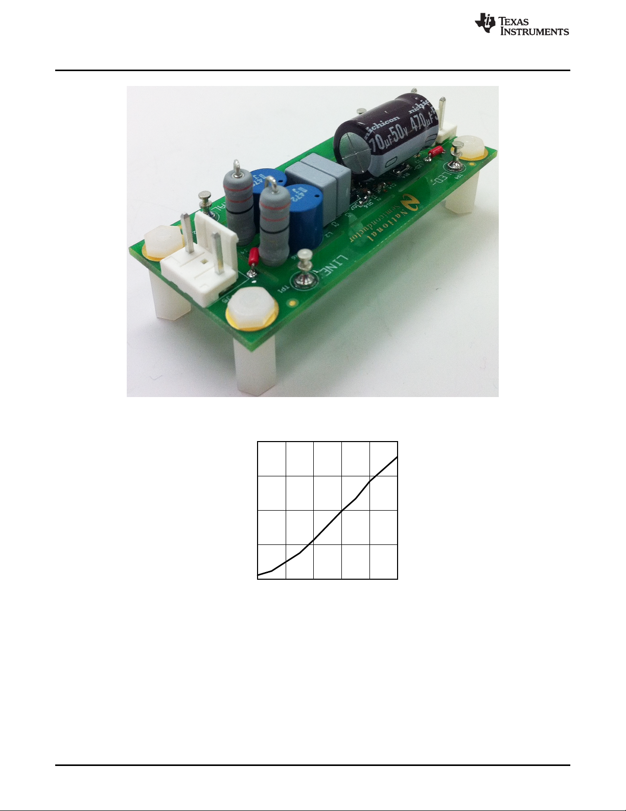
Figure 1. Demo Board
Figure 2. LED Current vs. Line Voltage (using TRIAC Dimmer)
2
AN-2127 LM3448 A19 Edison Retrofit Evaluation Board SNOA559B–October 2011–Revised May 2013
Copyright © 2011–2013, Texas Instruments Incorporated
Submit Documentation Feedback
Page 3
80 90 100 110 120 130 140
50
100
150
200
250
300
350
LED CURRENT (mA)
INPUT VOLTAGE (V
RMS
)
12 LEDs
10 LEDs
8 LEDs
80 90 100 110 120 130 140
4
5
6
7
8
P
OUT
(W)
INPUT VOLTAGE V
RMS
12 LEDs
10 LEDs
8 LEDs
80 90 100 110 120 130 140
74
76
78
80
82
84
EFFICIENCY (%)
INPUT VOLTAGE (V
RMS
)
12 LEDs
10 LEDs
8 LEDs
80 90 100 110 120 130 140
0.78
0.80
0.82
0.84
0.86
0.88
0.90
POWER FACTOR
INPUT VOLTAGE V
RMS
12 LEDs
10 LEDs
8 LEDs
www.ti.com
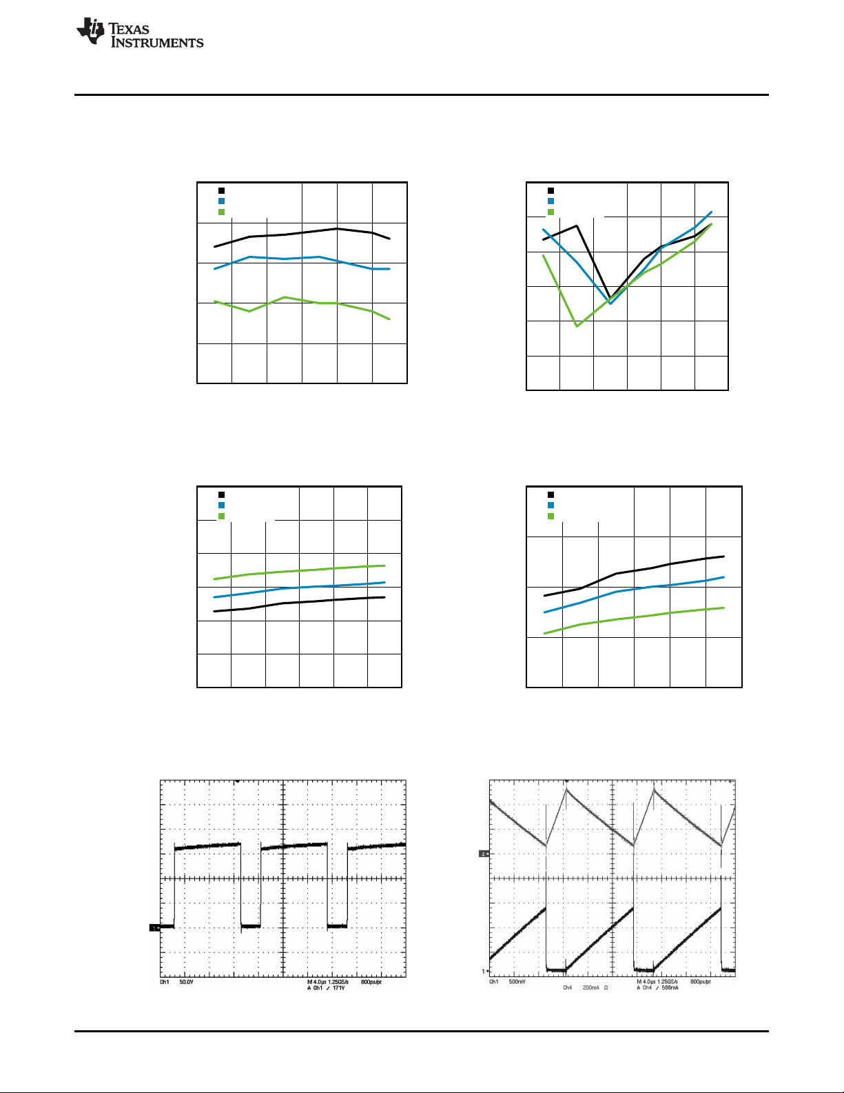
5 Typical Performance Characteristics
TJ=25°C and VCC=12V, unless otherwise specified.
Figure 3. Efficiency vs. Line Voltage Figure 4. Power Factor vs. Line Voltage
Typical Performance Characteristics
Figure 5. LED Current vs. Line Voltage Figure 6. Output Power vs. Line Voltage
Figure 7. SW FET Drain Voltage Waveform Figure 8. COFF Voltage (CH1), Inductor Current (CH4)
(VIN=120V
SNOA559B–October 2011–Revised May 2013 AN-2127 LM3448 A19 Edison Retrofit Evaluation Board
Submit Documentation Feedback
RMS
, 12 LEDs, I
=181mA) (VIN=120V
LED
Copyright © 2011–2013, Texas Instruments Incorporated
, 12 LEDs, I
RMS
LED
=181mA)
3
Page 4
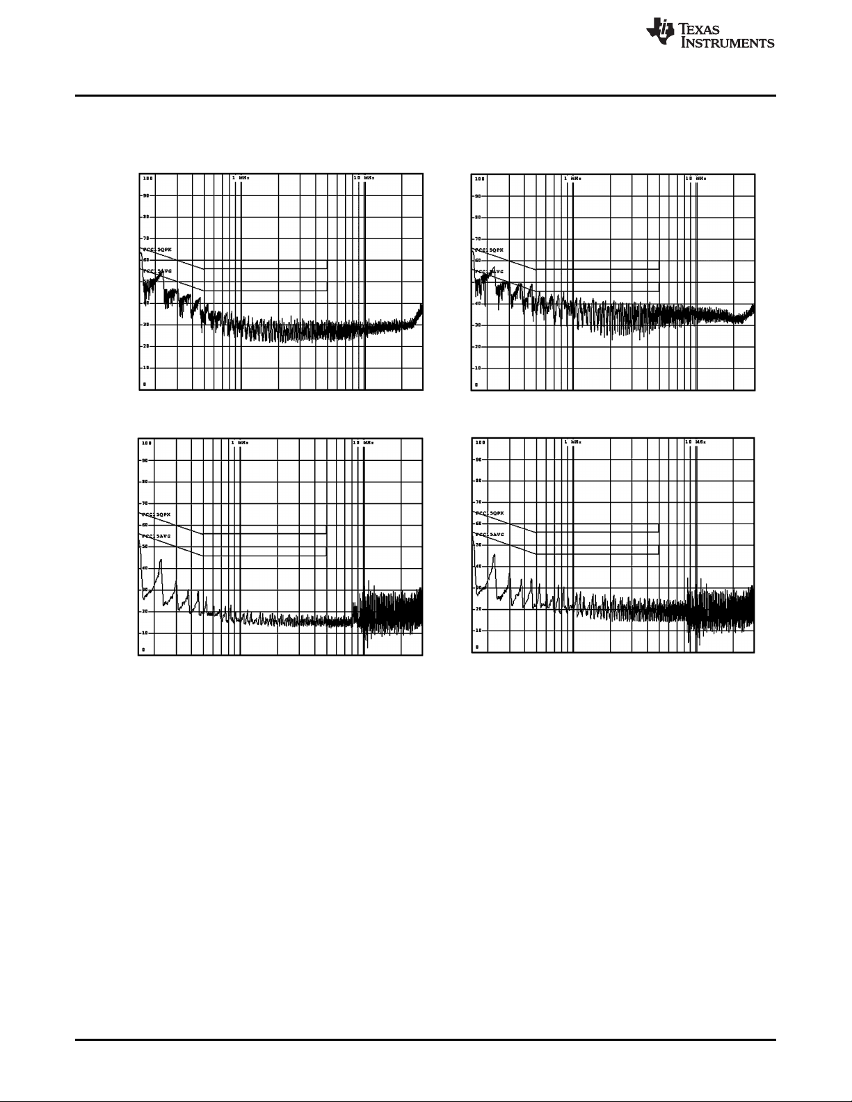
EMI Performance
6 EMI Performance
120V, 6.5W Conducted EMI Scans
Figure 9. LINE – CISPR/FCC Class B Peak Scan Figure 10. NEUTRAL – CISPR/FCC Class B Peak Scan
www.ti.com
Figure 11. LINE – CISPR/FCC Class B Average Scan Figure 12. NEUTRAL – CISPR/FCC Class B Average
Scan
4
AN-2127 LM3448 A19 Edison Retrofit Evaluation Board SNOA559B–October 2011–Revised May 2013
Copyright © 2011–2013, Texas Instruments Incorporated
Submit Documentation Feedback
Page 5
www.ti.com
Circuit Operation With Forward Phase TRIAC Dimmer
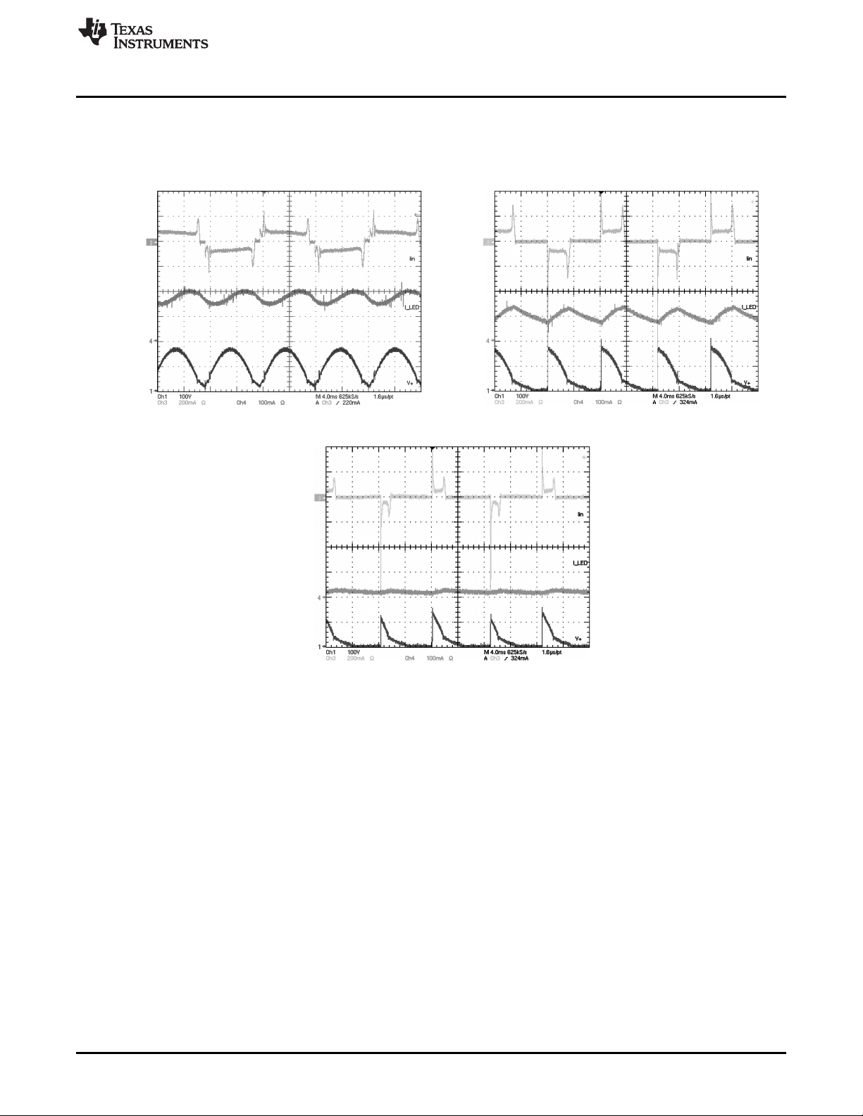
7 Circuit Operation With Forward Phase TRIAC Dimmer
The dimming operation of the circuit was verified using a forward phase TRIAC dimmer. Waveforms
captured at different dimmer settings are shown below:
Figure 13. Forward phase circuit at full brightness Figure 14. Forward phase circuit at 90° firing angle
Figure 15. Forward phase circuit at 135° firing angle
SNOA559B–October 2011–Revised May 2013 AN-2127 LM3448 A19 Edison Retrofit Evaluation Board
Submit Documentation Feedback
Copyright © 2011–2013, Texas Instruments Incorporated
5
Page 6
Circuit Operation With Reverse Phase Dimmer
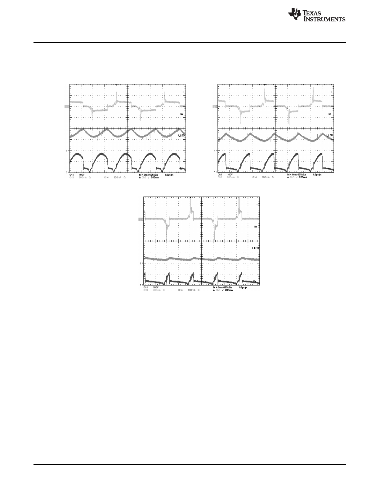
8 Circuit Operation With Reverse Phase Dimmer
The circuit operation was also verified using a reverse phase dimmer and waveforms captured at different
dimmer settings are shown below:
Figure 16. Reverse phase circuit at full brightness Figure 17. Reverse phase circuit at 90° firing angle
www.ti.com
Figure 18. Reverse phase circuit at 135° firing angle
6
AN-2127 LM3448 A19 Edison Retrofit Evaluation Board SNOA559B–October 2011–Revised May 2013
Copyright © 2011–2013, Texas Instruments Incorporated
Submit Documentation Feedback
Page 7
www.ti.com
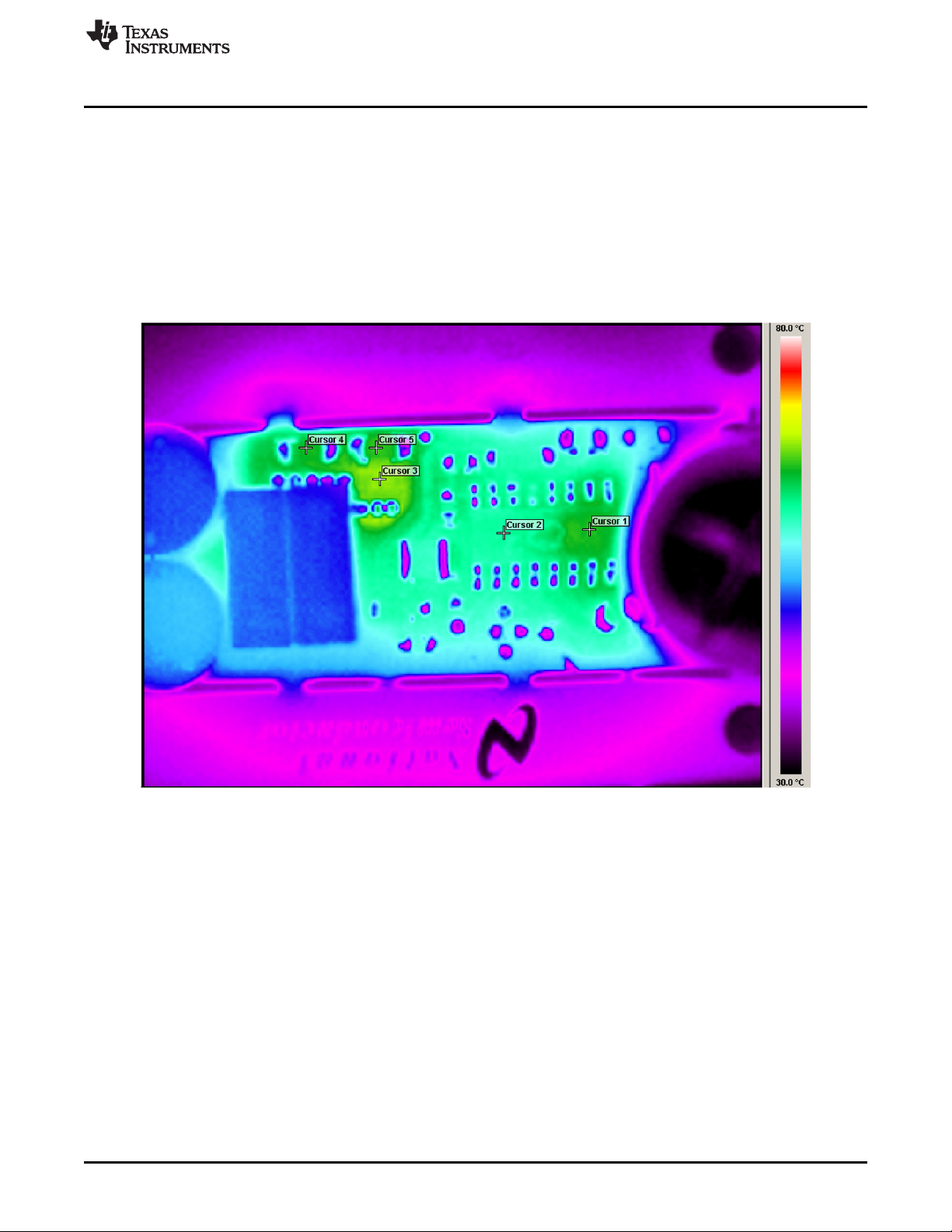
9 Thermal Performance
The board temperature was measured using an IR camera (HIS-3000, Wahl) while running under the
following conditions: VIN= 120V
NOTE: Thermal performance is highly dependent on the user's final end-application enclosure, heatsinking methods, ambient operating temperature, and PCB board layout in addition to the electrical
operating conditions. This LM3448 evaluation board is optimized to supply 6.5W of output power at room
temperature without exceeding the thermal limitations of the LM3448. However higher output power levels
can be achieved if precautions are taken not to exceed the power dissipation limits of the LM3448
package or die junction temperature. Please see the LM3448 datasheet for additional details regarding its
thermal specifications.
RMS
, I
= 181mA, # of LEDs = 12, P
LED
OUT
Thermal Performance
= 6.5W.
• Cursor 1: 65.3°C
• Cursor 2: 60.1°C
• Cursor 3: 67.6°C
• Cursor 4: 64.9°C
• Cursor 5: 65.6°C
Figure 19. Top Side - Thermal Scan
SNOA559B–October 2011–Revised May 2013 AN-2127 LM3448 A19 Edison Retrofit Evaluation Board
Submit Documentation Feedback
Copyright © 2011–2013, Texas Instruments Incorporated
7
Page 8
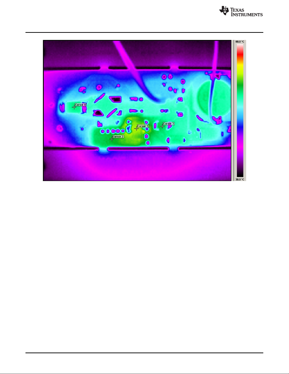
Thermal Performance
www.ti.com
• Cursor 1: 68.1°C
• Cursor 2: 64.7°C
• Cursor 3: 62.6°C
• Cursor 4: 61.7°C
Figure 20. Bottom Side - Thermal Scan
8
AN-2127 LM3448 A19 Edison Retrofit Evaluation Board SNOA559B–October 2011–Revised May 2013
Copyright © 2011–2013, Texas Instruments Incorporated
Submit Documentation Feedback
Page 9
1
4
3
2
16
13
14
15
ASNS
DIM
GND
FLTR1
COFF
FLTR2
5 12
BLDR
ISNS
11
NC
NC
VCC
GND
10
8 9
SW
SW
6
7
SW
SW
www.ti.com
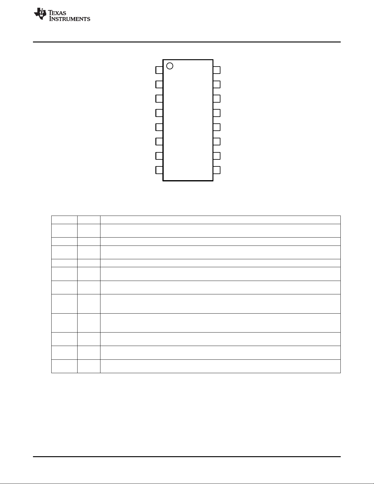
10 LM3448 Device Pin-Out
Pin # Name Description
1, 2, 15, SW Drain connection of internal 600V MOSFET.
16
3, 14 NC No connect. Provides clearance between high voltage and low voltage pins. Do not tie to GND.
4 BLDR Bleeder pin. Provides the input signal to the angle detect circuitry. A 230Ω internal resistor ensures BLDR is
5, 12 GND Circuit ground connection.
6 V
7 ASNS PWM output of the TRIAC dim decoder circuit. Outputs a 0 to 4V PWM signal with a duty cycle proportional
8 FLTR1 First filter input. The 120Hz PWM signal from ASNS is filtered to a DC signal and compared to a 1 to 3V,
9 DIM Input/output dual function dim pin. This pin can be driven with an external PWM signal to dim the LEDs. It
10 COFF OFF time setting pin. A user set current and capacitor connected from the output to this pin sets the
11 FLTR2 Second filter input. A capacitor tied to this pin filters the PWM dimming signal to supply a DC voltage to
13 ISNS LED current sense pin (internally connected to MOSFET source). Connect a resistor from ISNS to GND to
pulled down for proper angle sense detection.
Input voltage pin. This pin provides the power for the internal control circuitry and gate driver. Connect a
CC
22µF (minimum) bypass capacitor to ground.
to the TRIAC dimmer on-time.
5.85 kHz ramp to generate a higher frequency PWM signal with a duty cycle proportional to the TRIAC
dimmer firing angle. Pull above 4.9V (typical) to TRI-STATE® DIM.
may also be used as an output signal and connected to the DIM pin of other LM3448/LM3445 devices or
LED drivers to dim multiple LED circuits simultaneously.
constant OFF time of the switching controller.
control the LED current. Could also be used as an analog dimming input.
set the maximum LED current.
LM3448 Device Pin-Out
Figure 21. Device Pin-Out
Table 1. Pin Description 16 Pin Narrow SOIC
SNOA559B–October 2011–Revised May 2013 AN-2127 LM3448 A19 Edison Retrofit Evaluation Board
Submit Documentation Feedback
Copyright © 2011–2013, Texas Instruments Incorporated
9
Page 10

LED +
LED - LINE
NEUTRAL
J10
J5
TP4
TP3
TP1
TP2
Demo Board Wiring Overview
11 Demo Board Wiring Overview
Figure 22. Wiring Connection Diagram
Test Name I/O Description
Point
TP3 LED + Output LED Constant Current Supply
TP4 LED - Output LED Return Connection (not GND)
TP1 LINE Input AC Line Voltage
TP2 NEUTRAL Input AC Neutral
www.ti.com
Table 2. Test Points
Supplies voltage and constant-current to anode of LED string.
Connects to cathode of LED string. Do NOT connect to GND.
Connects directly to AC line or output of TRIAC dimmer of a 120VAC system.
Connects directly to AC neutral of a 120VAC system.
12 Demo Board Assembly
Figure 23. Top View
10
AN-2127 LM3448 A19 Edison Retrofit Evaluation Board SNOA559B–October 2011–Revised May 2013
Copyright © 2011–2013, Texas Instruments Incorporated
Submit Documentation Feedback
Page 11

R15 C15
R2
R7
R1
R3
D7
Q1
R8
DIM
COFF
FLTR2
GND
ISNS
FLTR1
ASNS
BLDR
VCC
GND
LM3448
9
10
11
12
13
8
7
6
5
4
V+
C8
V
CC
R22 D8
R14
+
V
LED+
V
LED±
L1
C6
D2
V+
LINE
NEUTRAL
LINE EMI FILTER
D4
C4
C3
COFF
R16
C12
L2
C2
C
OFF
Current Source
C1
L3
C16
R4
C10
C14
R6
R5
D1
C5
NC
SW
SW
NC
SW
SW
14
15
16
3
2
1
R9
COFF
C13
U1
V
CC
www.ti.com
13 Design Guide
Design Guide
Figure 24. Bottom View
SNOA559B–October 2011–Revised May 2013 AN-2127 LM3448 A19 Edison Retrofit Evaluation Board
Submit Documentation Feedback
Figure 25. Evaluation Board Schematic
Copyright © 2011–2013, Texas Instruments Incorporated
11
Page 12

R15
C15
R2
R7
V+
LM3448
11 FLTR2
C14
V
INJECT
t
V
INJECT
Design Guide
13.1 Buck Converter
The following section explains how to design a non-isolated buck converter using the LM3448. Refer to
the LM3448 datasheet for specific details regarding the function of the LM3448 device. All reference
designators refer to the Evaluation Board Schematic in Figure 25 unless otherwise noted. The circuit
operates in open-loop based on a constant off-time that is set by selecting appropriate circuit components.
Like an incandescent lamp, the driver is compatible with both forward and reverse phase dimmers.
AC-Coupled Line Injection
By injecting a voltage V
input current shaping is obtained which improves power factor performance. By AC-coupling the V
signal through capacitor C14, improved line-regulation of the LED current is also achieved (see
Figure 27).
which is proportional to the line voltage into the FLTR2 pin (see Figure 26),
INJECT
Figure 26. FLTR2 Waveform with No Dimmer
www.ti.com
INJECT
12
Figure 27. AC-Coupled Line-Injection Circuit
Figure 28 shows how line shaping of the input current is implemented. Peak voltage at the FLTR2 pin
should be kept below 1.25V otherwise current limit will be tripped. A good starting point is to set up the
resistor divider consisting of resistors R2, R7 and R15 to provide a V
peak input voltage of 1.0V at
INJECT
the input of capacitor C14 at the nominal input voltage. Recommended values for the AC-coupling
capacitor C14 is 0.47µF and for the FLTR2 capacitor C15 is 0.1µF.
With a 1.0V V
voltage, the voltage at the FLTR2 pin at the maximum and minimum input voltages can
INJECT
be calculated using the following equations,
(1)
These V
voltages will be used later to determine ripple and peak inductor currents.
FLTR2
AN-2127 LM3448 A19 Edison Retrofit Evaluation Board SNOA559B–October 2011–Revised May 2013
Copyright © 2011–2013, Texas Instruments Incorporated
Submit Documentation Feedback
Page 13

R
FLTR1
R
SNS
PWM
I-LIM
1.27V
ISNS
ASNS
GND
FLTR1
FLTR2
DIM
DIM DECODER
4.9V
Tri-State
50k
370k
C
FLTR2
C
FLTR1
1k
RAMP GEN.
5.9 kHz
3V
1V
750 mV
125 ns
LEADING EDGE BLANKING
1V
The PWM reference increases
as the line voltage increases.
As line voltage increases, the voltage across the
inductor increases, and the peak current increases.
LED Current
RAMP
www.ti.com
Off-time, On-time and Switching Frequency
The AC mains voltage at the line frequency fLis assumed to be perfectly sinusoidal and the diode bridge
ideal. This yields a perfect rectified sinusoid at the input to the buck converter. The maximum, nominal and
minimum peak input voltages are defined as follows,
Design Guide
Figure 28. Typical Operation of FLTR2 Pin
The LM3448 will operate as a constant off-time regulator, and so t
will be constant throughout all
OFF
operating points. The on-time tON(and subsequently the switching frequency fSW) will vary depending on
input voltage and LED stack voltage values. For this buck converter operating in continuous conduction
mode (CCM), the minimum on-time t
f
at the maximum peak input voltage,
SW(MAX)
The off-time t
It is important to note that there is a minimum on-time of 200ns that needs to be met in order for proper
is now calculated where T
OFF
LED driver operation.
SNOA559B–October 2011–Revised May 2013 AN-2127 LM3448 A19 Edison Retrofit Evaluation Board
Submit Documentation Feedback
Copyright © 2011–2013, Texas Instruments Incorporated
can be determined for a maximum desired switching frequency
ON(MIN)
is the minimum switching period,
S(MIN)
(2)
(3)
(4)
13
Page 14

R
SNS
(W)
I
LED
(mA)
400
370
340
310
280
250
220
190
160
P
OUT
(W)
9.8
9.1
8.3
7.6
6.8
6.1
5.3
4.6
2.62.52.42.32.22.12.01.91.81.71.61.51.41.3
3.8
R
SNS
(W)
I
LED
(mA)
270
250
230
210
190
170
150
130
110
P
OUT
(W)
9.8
9.1
8.3
7.6
6.8
6.1
5.3
4.6
2.62.52.42.32.22.12.01.91.81.71.61.51.41.3
3.8
R
SNS
(W)
I
LED
(mA)
322
298
274
250
226
202
178
154
130
P
OUT
(W)
9.8
9.1
8.3
7.6
6.8
6.1
5.3
4.6
2.62.52.42.32.22.12.01.91.81.71.61.51.41.3
3.8
Design Guide
Output Power and Current Sense Resistor
Due to the interaction of the AC-coupled line-injection voltage with the FLTR2 signal, the equations for
determining the correct sense resistor R
desired output power P
graphs showing the relationship between LED current, P
and Figure 31 for common stack voltages of 8, 10 and 12 LEDs. By referring to these graphs, users can
choose R14 values that will meet their LED current and output power requirements.
(shown as R14 in the evaluation board schematic) for a
are complex and beyond the scope of this document. Instead, performance
OUT
SNS
OUT
and R
are shown in Figure 29, Figure 30
SNS
www.ti.com
Figure 29. I
LED
vs. P
OUT
vs. R
SNS
Figure 30. I
LED
for 12 LEDs (Vf=3.0V) for 10 LEDs (Vf=3.0V)
Figure 31. I
LED
vs. P
OUT
vs. R
SNS
for 8 LEDs (Vf=3.0V)
Inductor
Peak inductor currents will need to be calculated as shown below based on the V
sense resistor R14 at the maximum and minimum peak input voltages,
vs. P
vs. R
OUT
FLTR2
SNS
voltages and chosen
14
AN-2127 LM3448 A19 Edison Retrofit Evaluation Board SNOA559B–October 2011–Revised May 2013
Copyright © 2011–2013, Texas Instruments Incorporated
Submit Documentation Feedback
(5)
Page 15

COFF
R16
C12
V
CC
www.ti.com
Inductor ripple current will need to be specified by the user based on desired EMI performance, inductor
size and other operating conditions. The following equations show how to calculate for maximum and
minimum inductor ripple currents respectively by basing the ripple (i.e.Δi
peak inductor currents,
It is recommended that this buck converter design operate in CCM over the full range of operating peak
input voltages, and so the minimum inductor peak current at V
The inductor value can be calculated based on the minimum on-time, LED output voltage and the
specified inductor ripple current Δi
COFF Current Source
The current source used to establish the constant off-time is shown in Figure 32.
L-PK(VIN-PK-MAX)
Design Guide
as a percentage of maximum
L(%)
IN-PK(MIN)
should not go below zero,
at the maximum peak input voltage as described below,
(6)
(7)
(8)
Figure 32. COFF Current Source Circuit
Capacitor C12 will be charged with current from the VCCsupply through resistor R16. The COFF pin
threshold will therefore be tripped based on the following capacitor equation,
(9)
where,
(10)
Solving for off-time t
SNOA559B–October 2011–Revised May 2013 AN-2127 LM3448 A19 Edison Retrofit Evaluation Board
Submit Documentation Feedback
results in,
OFF
(11)
15
Copyright © 2011–2013, Texas Instruments Incorporated
Page 16

Design Guide
Re-arranging the above equation results in R16 being calculated where C12 is typically chosen as value
around 470pF,
Additionally, the maximum on-time t
maximum switching period T
calculated inductor value, these values can now be calculated as,
Maximum and minimum duty cycles, D
voltages respectively,
and corresponding minimum switching frequency f
ON(MAX)
occur at the minimum peak input voltage. Using the previously
S(MAX)
MAX
and D
, will occur at the minimum and maximum peak input
MIN
SW(MIN)
www.ti.com
(12)
and
(13)
(14)
Switching MOSFET (SW FET)
Peak and RMS SW FET currents are calculated along with maximum SW FET power dissipation based on
the SW FET R
value using the following equations,
DS-ON
(15)
(16)
and,
(17)
Current Limit
The peak inductor current limit I
should be approximately 25% higher than the maximum operating peak
LIM
inductor current,
(18)
The sense resistor will need to be able to dissipate the maximum power,
16
(19)
AN-2127 LM3448 A19 Edison Retrofit Evaluation Board SNOA559B–October 2011–Revised May 2013
Copyright © 2011–2013, Texas Instruments Incorporated
Submit Documentation Feedback
Page 17

www.ti.com
Re-circulating Diode
The main re-circulating diode (D4) should be sized to block the maximum reverse voltage V
operate at the maximum peak I
P
as determined by the following equations,
D4(MAX)
DR-PK(MAX)
NOTE: For proper converter operation, the chosen diode should have a reverse recovery time that is less
than the LM3448's leading edge blanking time of 125ns.
13.2 Bias Supplies and Capacitances
The VCC bias supply circuit is shown in Figure 33. The passFET (Q1) is used in its linear region to standoff the line voltage from the LM3448 regulator. Both the VCC startup current and discharging of the EMI
filter capacitance for proper phase angle detection are handled by Q1. Therefore Q1 has to block the
maximum peak input voltage and have both sufficient surge and power handling capability with regards to
its safe operating area (SOA). The design equations are,
and RMS currents I
D4-RMS(MAX)
Design Guide
,
RD4(MAX)
, and dissipate the maximum power
(20)
(21)
(22)
(23)
Note that if additional TRIAC holding current is to be sourced through Q1, then the transistor will need to
be sized appropriately to handle the additional current and power dissipation requirements.
(24)
(25)
(26)
SNOA559B–October 2011–Revised May 2013 AN-2127 LM3448 A19 Edison Retrofit Evaluation Board
Submit Documentation Feedback
Copyright © 2011–2013, Texas Instruments Incorporated
17
Page 18

R3
D7
Q1
R8
V+
C8
R22
D8
LM3448
6VCC
R1
V
CC
Design Guide
www.ti.com
Figure 33. Bias Supply Circuit
Input Capacitance
The input capacitors C1 and C10 have to be able to provide energy during the worst-case switching period
at the peak of the AC voltage input. They should be high frequency, high stability capacitors (usually
metallized film capacitors, either polypropylene or polyester) with an AC voltage rating equal to the
maximum input voltage. They should also have a DC voltage rating exceeding the maximum peak input
voltage plus half of the peak to peak input voltage ripple specification. The minimum required input
capacitance is calculated given the same ripple specification,
(27)
Output Capacitance
C3 should be a high quality electrolytic capacitor with a voltage rating greater than the specified LED stack
voltage. Given the desired voltage ripple, the minimum output capacitance is calculated,
(28)
13.3 Input Filter
Background
Since the LM3448 is used for AC to DC systems, electromagnetic interference (EMI) filtering is critical to
pass the necessary standards for both conducted and radiated EMI. This filter will vary depending on the
output power, the switching frequencies, and the layout of the PCB. There are two major components to
EMI: differential noise and common-mode noise. Differential noise is typically represented in the EMI
spectrum below approximately 500kHz while common-mode noise shows up at higher frequencies.
18
AN-2127 LM3448 A19 Edison Retrofit Evaluation Board SNOA559B–October 2011–Revised May 2013
Copyright © 2011–2013, Texas Instruments Incorporated
Submit Documentation Feedback
Page 19

L1
C6
D2
V+
LINE
NEUTRAL
L2
C2
C16
R4
R6
R5
C5
www.ti.com
Conducted
Figure 34 shows a typical filter used with this LM3448 flyback design. In order to conform to conducted
standards, a fourth order filter is implemented using inductors and "X" rated AC capacitors. If sized
properly, this filter design can provide ample attenuation of the switching frequency and lower order
harmonics contributing to differential noise. This combination of filter components along with any
necessary damping can easily provide a passing conducted EMI signature.
Radiated
Conforming to radiated EMI standards is much more difficult and is completely dependent on the entire
system including the enclosure. Reduction of dV/dt on switching edges and PCB layout iterations are
frequently necessary. Consult available literature and/or an EMI specialist for help with this. Several
iterations of component selection and layout changes may be necessary before passing a specific
radiated EMI standard.
Interaction with Dimmers
In general input filters and forward phase dimmers do not work well together. The TRIAC needs a
minimum amount of holding current to function. The converter itself is demanding a certain amount of
current from the input to provide to its output, and the input filter is providing or taking current depending
upon the dV/dt of the capacitors. The best way to deal with this problem is to minimize filter capacitance
and increase the regulated hold current until there is enough current to satisfy the dimmer and filter
simultaneously.
Design Guide
Figure 34. Input EMI Filter
13.4 Inrush Limiting and Damping
Inrush
With a forward phase dimmer, a very steep rising edge causes a large inrush current every cycle as
shown in Figure 35. Series resistance (R5, R6) can be placed between the filter and the TRIAC to limit the
effect of this current on the converter and to provide some of the necessary holding current at the same
time. This will degrade efficiency but some inrush protection is always necessary in any AC system due to
startup. The size of R5 and R6 are best found experimentally as they provide attenuation for the whole
system.
SNOA559B–October 2011–Revised May 2013 AN-2127 LM3448 A19 Edison Retrofit Evaluation Board
Submit Documentation Feedback
Copyright © 2011–2013, Texas Instruments Incorporated
19
Page 20

t
Iin(t)
0
Potential Misfire
Triac Fires Æ Inrush Spike
Design Calculations
Damper
The inrush spike can also excite a resonance between the input filter of the TRIAC and the input filter of
the converter. The associated interaction can cause the current to ring negative, as shown in Figure 35,
thereby shutting off the TRIAC. A TRIAC damper can be placed between the dimmer and the EMI filter to
absorb some of the ringing energy and reduce the potential for misfires. The damper is also best sized
experimentally due to the large variance in TRIAC input filters. Resistors R5 and R6 can also be increased
to help dampen the ringing at the expense of some efficiency and power factor performance.
www.ti.com
Figure 35. Inrush Current Spike
14 Design Calculations
The following is a step-by-step procedure with calculations for a 120V, 6.5W non-isolated buck converter
design.
14.1 Specifications
V
V
V
P
V
I
LED
Efficiency,η = 80%
fL= 60Hz
f
SW(MAX)
T
Δv
Δv
SW FET V
SW FET R
V
VCC= 12V
IN(MAX)
IN(NOM)
IN(MIN)
= 6.5W
OUT
= 36V
OUT
= 181mA
S(MIN)
= 1V
OUT
IN-PK
= 0.8V
f(D4)
= 135VAC
= 120VAC
= 85VAC
=75kHz
=13.33µs
= 35V
DS(MAX)
DS-ON
= 600V
= 3.5Ω
20
AN-2127 LM3448 A19 Edison Retrofit Evaluation Board SNOA559B–October 2011–Revised May 2013
Copyright © 2011–2013, Texas Instruments Incorporated
Submit Documentation Feedback
Page 21

www.ti.com
V
=12V
Z(D7)
R8=49.9kΩ
V
=0.7V
GS(Q1)
14.2 Preliminary Calculations
Nominal peak input voltage:
Calculate minimum on-time and verify it's greater than 200ns:
Calculate off-time:
From Figure 29, choose R14=2.0Ω for 6.5W output power with 12 LEDs.
Design Calculations
(29)
(30)
(31)
14.3 FLTR2 AC-LINE Injection
Choose V
INJECT(NOM)
Choose R2=R7=274kΩ
Calculate R15:
or,
Calculate maximum FLTR2 pin voltage and verify it is less than 1.25V:
Calculate minimum FLTR2 pin voltage:
=1.0V
(32)
(33)
(34)
(35)
SNOA559B–October 2011–Revised May 2013 AN-2127 LM3448 A19 Edison Retrofit Evaluation Board
Submit Documentation Feedback
Copyright © 2011–2013, Texas Instruments Incorporated
21
Page 22

Design Calculations
14.4 Inductor
Calculate peak inductor currents at the minimum and maximum peak input voltages:
Calculate inductor ripple currents at the minimum and maximum peak input voltages based on 80% of
maximum peak inductor currents:
Verify that converter is in CCM operation at the minimum peak input voltage:
Calculate inductor value:
www.ti.com
(36)
(37)
(38)
14.5 COFF Current Source
Choose capacitor C12=470pF.
Calculate resistor R16:
Calculate maximum on-time, minimum switching frequency and maximum switching period:
Calculate maximum and minimum duty cycles:
(39)
(40)
(41)
22
(42)
AN-2127 LM3448 A19 Edison Retrofit Evaluation Board SNOA559B–October 2011–Revised May 2013
Copyright © 2011–2013, Texas Instruments Incorporated
Submit Documentation Feedback
Page 23

www.ti.com
14.6 SW FET
Calculate maximum peak SW FET current:
Calculate maximum RMS SW FET current:
Calculate maximum power dissipation:
14.7 Current Limit
Calculate peak inductor current limit:
Power dissipation:
Resulting component choice:
Design Calculations
(43)
(44)
(45)
(46)
(47)
14.8 Re-circulating Diode
Maximum reverse blocking voltage:
Maximum peak diode current:
Maximum RMS diode current:
Maximum power dissipation:
Resulting component choice:
(48)
(49)
(50)
(51)
(52)
(53)
SNOA559B–October 2011–Revised May 2013 AN-2127 LM3448 A19 Edison Retrofit Evaluation Board
Submit Documentation Feedback
Copyright © 2011–2013, Texas Instruments Incorporated
23
Page 24

Design Calculations
14.9 PassFET
Calculate maximum peak voltage:
Calculate current:
Calculate maximum power dissipation:
Resulting component choice:
14.10 Input Capacitance
Minimum capacitance:
www.ti.com
(54)
(55)
(56)
(57)
AC Voltage rating:
DC Voltage rating:
Resulting component choice:
14.11 Output Capacitance
Minimum capacitance:
Voltage rating:
Resulting component choice:
(58)
(59)
(60)
(61)
(62)
(63)
24
(64)
AN-2127 LM3448 A19 Edison Retrofit Evaluation Board SNOA559B–October 2011–Revised May 2013
Copyright © 2011–2013, Texas Instruments Incorporated
Submit Documentation Feedback
Page 25

R15 C15
R2
R7
R1
R3
D7
Q1
R8
DIM
COFF
FLTR2
GND
ISNS
FLTR1
ASNS
BLDR
VCC
GND
LM3448
9
10
11
12
13
8
7
6
5
4
V+
C8
V
CC
R22 D8
R14
+
V
LED+
V
LED±
L1
C6
D2
V+
LINE
NEUTRAL
LINE EMI FILTER
D4
C4
C3
COFF
R16
C12
L2
C2
C
OFF
Current Source
C1
L3
C16
R4
C10
C14
R6
R5
D1
C5
NC
SW
SW
NC
SW
SW
14
15
16
3
2
1
R9
COFF
C13
U1
V
CC
www.ti.com
15 Evaluation Board Schematic
Evaluation Board Schematic
The LM3448 evaluation board has exposed high voltage
components that present a shock hazard. Caution must be taken
when handling the evaluation board. Avoid touching the evaluation
board and removing any cables while the evaluation board is
operating. Isolating the evaluation board rather than the
oscilloscope is highly recommended.
WARNING
SNOA559B–October 2011–Revised May 2013 AN-2127 LM3448 A19 Edison Retrofit Evaluation Board
Submit Documentation Feedback
Copyright © 2011–2013, Texas Instruments Incorporated
25
Page 26

Bill of Materials
16 Bill of Materials
Part ID Description Manufacturer Part Number
C1, C10 CAP CER 47000PF 500V X7R 1210 Johanson Dielectrics 501S41W473KV4E
C2, C6 CAP FILM MKP .015UF 310VAC X2 Vishay/BC Comp BFC233820153
C3 CAP 470UF 50V ELECT PW RADIAL Nichicon UPW1H471MHD
C4 DNP DNP DNP
C5, C16 CAP CER .15UF 250V X7R 1210 TDK C3225X7R2E154K
C8 Ceramic, X5R, 16V, 20% MuRata GRM32ER61C476ME15L
C12 Ceramic, X7R, 50V, 10% MuRata GRM188R71H471KA01D
C13, C15 Ceramic, X7R, 16V, 10% MuRata GRM188R71C104KA01D
C14 Ceramic, X7R, 16V, 10% MuRata GRM188R71C474KA88D
D1, D8 DIODE SCHOTTKY 1A 200V PWRDI 123 Diodes Inc. DFLS1200-7
D2 RECT BRIDGE GP 400V 0.5A MINIDIP Diodes Inc. RH04DICT-ND
D4 DIODE FAST 1A 300V SMA Fairchild ES1F
D7 DIODE ZENER 15V 500MW SOD-123 Fairchild Semi MMSZ5245B
J5, J10 CONN HEADER .312 VERT 2POS TIN Tyco Electronics 1-1318301-2
L1, L2 INDUCTOR 4700UH .13A RADIAL TDK Corp TSL0808RA-472JR13-PF
L3 820uH, Shielded Drum Core, Coilcraft Inc. MSS1038-824KL
Q1 MOSFET N-CH 240V 260MA SOT-89 Infineon Technologies BSS87 L6327
R1, R3 1%, 0.25W Vishay-Dale CRCW1206200kFKEA
R2, R7 1%, 0.25W Vishay-Dale CRCW1206274kFKEA
R4 RES 430 OHM 1/2W 5% 2010 SMD Vishay\Dale CRCW2010430RJNEF
R5, R6 RES 33 OHM 3W 5% AXIAL TT Electronics/Welwyn ULW3-33RJA1
R8 1%, 0.1W Vishay-Dale CRCW060349K9FKEA
R9 1%, 0.1W Vishay-Dale CRCW060348K7FKEA
R14 RES, 2.00 ohm, 1%, 0.25W, 1206 Vishay-Dale CRCW12062R00FNEA
R15 RES, 3.16k ohm, 1%, 0.1W, 0603 Vishay-Dale CRCW06033K16FKEA
R16 RES, 226k ohm, 1%, 0.1W, 0603 Vishay-Dale CRCW0603226KFKEA
R22 1%, 0.125W Vishay-Dale CRCW080540R2FKEA
TP1, TP2, Terminal, Turret, TH, Double Keystone Electronics 1502-2
TP3, TP4
U1 LM3448 LED Driver Texas Instruments LM3448
www.ti.com
26
AN-2127 LM3448 A19 Edison Retrofit Evaluation Board SNOA559B–October 2011–Revised May 2013
Copyright © 2011–2013, Texas Instruments Incorporated
Submit Documentation Feedback
Page 27

www.ti.com
17 PCB Layout
NOTE: Spacing between traces and components of this evaluation board are based on high voltage
recommendations for designs that will be potted. Users are cautioned to satisfy themselves as to the
suitability of this design for the intended end application and take any necessary precautions where high
voltage layout and spacing rules must be followed.
PCB Layout
Figure 36. Top Layer
Figure 37. Bottom Layer
SNOA559B–October 2011–Revised May 2013 AN-2127 LM3448 A19 Edison Retrofit Evaluation Board
Submit Documentation Feedback
Copyright © 2011–2013, Texas Instruments Incorporated
27
Page 28

IMPORTANT NOTICE
Texas Instruments Incorporated and its subsidiaries (TI) reserve the right to make corrections, enhancements, improvements and other
changes to its semiconductor products and services per JESD46, latest issue, and to discontinue any product or service per JESD48, latest
issue. Buyers should obtain the latest relevant information before placing orders and should verify that such information is current and
complete. All semiconductor products (also referred to herein as “components”) are sold subject to TI’s terms and conditions of sale
supplied at the time of order acknowledgment.
TI warrants performance of its components to the specifications applicable at the time of sale, in accordance with the warranty in TI’s terms
and conditions of sale of semiconductor products. Testing and other quality control techniques are used to the extent TI deems necessary
to support this warranty. Except where mandated by applicable law, testing of all parameters of each component is not necessarily
performed.
TI assumes no liability for applications assistance or the design of Buyers’ products. Buyers are responsible for their products and
applications using TI components. To minimize the risks associated with Buyers’ products and applications, Buyers should provide
adequate design and operating safeguards.
TI does not warrant or represent that any license, either express or implied, is granted under any patent right, copyright, mask work right, or
other intellectual property right relating to any combination, machine, or process in which TI components or services are used. Information
published by TI regarding third-party products or services does not constitute a license to use such products or services or a warranty or
endorsement thereof. Use of such information may require a license from a third party under the patents or other intellectual property of the
third party, or a license from TI under the patents or other intellectual property of TI.
Reproduction of significant portions of TI information in TI data books or data sheets is permissible only if reproduction is without alteration
and is accompanied by all associated warranties, conditions, limitations, and notices. TI is not responsible or liable for such altered
documentation. Information of third parties may be subject to additional restrictions.
Resale of TI components or services with statements different from or beyond the parameters stated by TI for that component or service
voids all express and any implied warranties for the associated TI component or service and is an unfair and deceptive business practice.
TI is not responsible or liable for any such statements.
Buyer acknowledges and agrees that it is solely responsible for compliance with all legal, regulatory and safety-related requirements
concerning its products, and any use of TI components in its applications, notwithstanding any applications-related information or support
that may be provided by TI. Buyer represents and agrees that it has all the necessary expertise to create and implement safeguards which
anticipate dangerous consequences of failures, monitor failures and their consequences, lessen the likelihood of failures that might cause
harm and take appropriate remedial actions. Buyer will fully indemnify TI and its representatives against any damages arising out of the use
of any TI components in safety-critical applications.
In some cases, TI components may be promoted specifically to facilitate safety-related applications. With such components, TI’s goal is to
help enable customers to design and create their own end-product solutions that meet applicable functional safety standards and
requirements. Nonetheless, such components are subject to these terms.
No TI components are authorized for use in FDA Class III (or similar life-critical medical equipment) unless authorized officers of the parties
have executed a special agreement specifically governing such use.
Only those TI components which TI has specifically designated as military grade or “enhanced plastic” are designed and intended for use in
military/aerospace applications or environments. Buyer acknowledges and agrees that any military or aerospace use of TI components
which have not been so designated is solely at the Buyer's risk, and that Buyer is solely responsible for compliance with all legal and
regulatory requirements in connection with such use.
TI has specifically designated certain components as meeting ISO/TS16949 requirements, mainly for automotive use. In any case of use of
non-designated products, TI will not be responsible for any failure to meet ISO/TS16949.
Products Applications
Audio www.ti.com/audio Automotive and Transportation www.ti.com/automotive
Amplifiers amplifier.ti.com Communications and Telecom www.ti.com/communications
Data Converters dataconverter.ti.com Computers and Peripherals www.ti.com/computers
DLP® Products www.dlp.com Consumer Electronics www.ti.com/consumer-apps
DSP dsp.ti.com Energy and Lighting www.ti.com/energy
Clocks and Timers www.ti.com/clocks Industrial www.ti.com/industrial
Interface interface.ti.com Medical www.ti.com/medical
Logic logic.ti.com Security www.ti.com/security
Power Mgmt power.ti.com Space, Avionics and Defense www.ti.com/space-avionics-defense
Microcontrollers microcontroller.ti.com Video and Imaging www.ti.com/video
RFID www.ti-rfid.com
OMAP Applications Processors www.ti.com/omap TI E2E Community e2e.ti.com
Wireless Connectivity www.ti.com/wirelessconnectivity
Mailing Address: Texas Instruments, Post Office Box 655303, Dallas, Texas 75265
Copyright © 2013, Texas Instruments Incorporated
 Loading...