

Page 1

AN-2061 LM3445 A19 Edison Retrofit Evaluation Board
1 Introduction
The evaluation board included in this shipment converts 85VACto 135VACinput and drives five to thirteen
series connected LED’s at the currents listed in the Evaluation Board Operating Conditions section. This is
a two-layer board using the bottom and top layer for component placement. The board is surrounded by a
larger area allowing for extra test points and connectors for ease of evaluation. The actual board size is
contained inside the larger outer area and can be cut out for the smallest size possible. The evaluation
board can be modified to adjust the LED forward current and the number of series connected LEDs. The
topology used for this evaluation board eliminates the need for passive power factor correction and results
in high efficiency and power factor with minimal component count which results in a size that can fit in a
standard A19 Edison socket. This board also operates correctly and dims smoothly using most standard
triac dimmers. Output current is regulated within ±15% of nominal from circuit to circuit and over line
voltage variation. For details on the LM3445 IC, see the LM3445 Triac Dimmable Offline LED Driver Data
Sheet (SNVS570).
A bill of materials shown in Table 2 describes the parts used on this demonstration board. A schematic
and layout have also been included along with measured performance characteristics including EMI/EMC
data. The above restrictions for the input voltage are valid only for the demonstration board as shipped
with the schematic below. for detailed information regarding the LM3445 device, see the LM3445 Triac
Dimmable Offline LED Driver Data Sheet (SNVS570). The board is currently set up to drive five to thirteen
series connected LEDs, but the evaluation board may be modified to accept more series LEDs. Refer to
the tables in this document to modify the board to accept more LEDs and/or adjust for different current
levels.
User's Guide
SNVA442C–June 2010–Revised May 2013
2 Evalution Board Operating Conditions
VIN= 85VACto 135V
5 to 13 series connected LEDs as configured with the currents listed below:
• Can drive up to 18 series LEDs (see table)
• I
• I
• I
• I
• I
All trademarks are the property of their respective owners.
= 340 mA (5 LEDs)
LED
= 300 mA (7 LEDs)
LED
= 260 mA (9 LEDs)
LED
= 230 mA (11 LEDs)
LED
= 205 mA (13 LEDs)
LED
AC
SNVA442C–June 2010–Revised May 2013 AN-2061 LM3445 A19 Edison Retrofit Evaluation Board
Submit Documentation Feedback
Copyright © 2010–2013, Texas Instruments Incorporated
1
Page 2
R15 C15
FLTR2
R2
R7
DIM
R9
COFF
C13
R1
R3
D7
Q1
R8
ASNS
FLTR1
DIM
COFF
FLTR2
BLDR
VCC
GND
GATE
ISNS
LM3445
1
2
3
4
5
10
9
8
7
6
V+
C8
V
CC
R22
D8
R12
R14
+
VLED+
VLED±
L1
C6
D2
V+
LINE NEUTRAL
LINE EMI FILTER
Q4
D4
C4
C3
V
CC
COFF
R16
C12
L2
C2
C
OFF
Current Source
C1
L3
C5
R4
C10
C14
RT1
F1
R6
R24
R5C9
D1
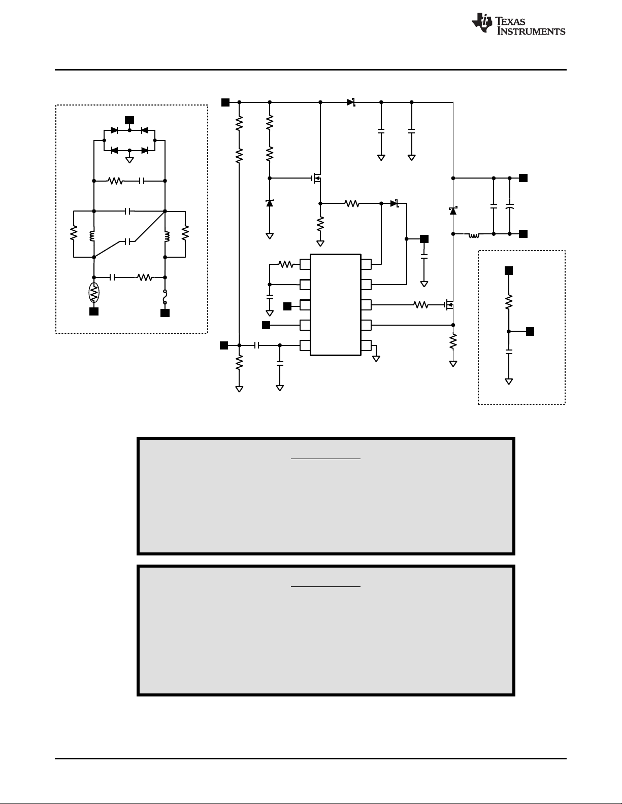
Simplified LM3445 Schematic
3 Simplified LM3445 Schematic
www.ti.com
WARNING
The LM3445 evaluation boards have no isolation or any type of
protection from shock. Caution must be taken when handling
evaluation board. Avoid touching evaluation board, and removing
any cables while evaluation board is operating. Isolating the
evaluation board rather than the oscilloscope is highly
recommended.
This LM3445 evaluation PCB is a non-isolated design. The ground
connection on the evaluation board is NOT referenced to earth
ground. If an oscilloscope ground lead is connected to the
evaluation board ground test point for analysis, and AC power is
applied, the fuse (F1) will fail open. The oscilloscope should be
powered via an isolation transformer before an oscilloscope
ground lead is connected to the evaluation board.
WARNING
2
AN-2061 LM3445 A19 Edison Retrofit Evaluation Board SNVA442C–June 2010–Revised May 2013
Copyright © 2010–2013, Texas Instruments Incorporated
Submit Documentation Feedback
Page 3
1
4
3
2
10
7
8
9
I
SNS
FLTR1
GATE
BLDR
COFF
V
CC
ASNS
DIM
5 6FLTR2 GND
www.ti.com
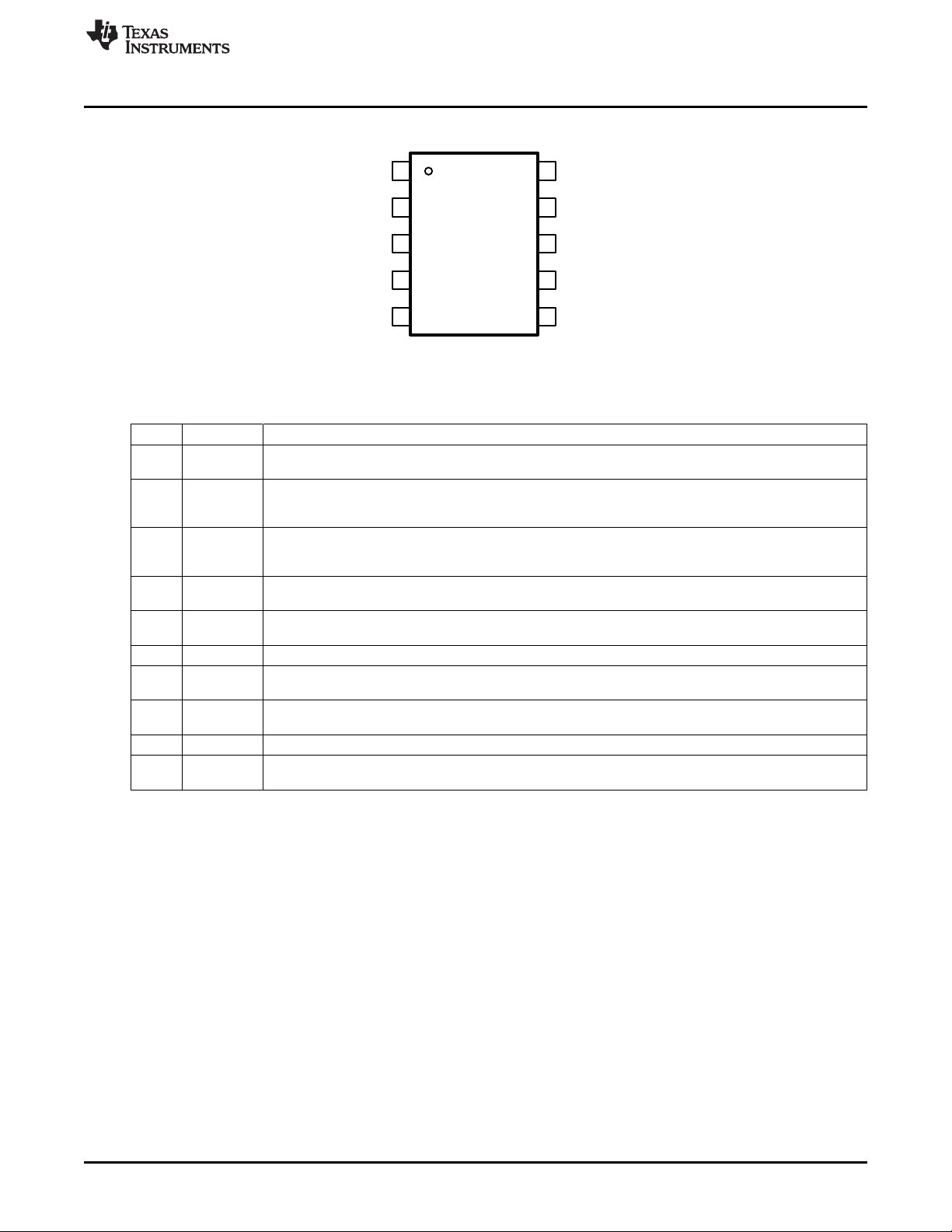
4 Pin-Out
Pin No Name Description
1 ASNS PWM output of the triac dim decoder circuit. Outputs a 0 to 4V PWM signal with a duty cycle proportional to
2 FLTR1 First filter input. The 120Hz PWM signal from ASNS is filtered to a DC signal and compared to a 1 to 3V,
3 DIM Input/output dual function dim pin. This pin can be driven with an external PWM signal to dim the LEDs. It
4 COFF OFF time setting pin. A user set current and capacitor connected from the output to this pin sets the
5 FLTR2 Second filter input. A capacitor tied to this pin filters the PWM dimming signal to supply a DC voltage to
6 GND Circuit ground connection.
7 ISNS LED current sense pin. Connect a resistor from main switching MOSFET source, ISNS to GND to set the
8 GATE Power MOSFET driver pin. This output provides the gate drive for the power switching MOSFET of the
9 V
10 BLDR Bleeder pin. Provides the input signal to the angle detect circuitry as well as a current path through a
Figure 1. 10-Pin VSSOP
Table 1. Pin Description 10 Pin VSSOP
the triac dimmer on-time.
5.85 kHz ramp to generate a higher frequency PWM signal with a duty cycle proportional to the triac
dimmer firing angle. Pull above 4.9V (typical) to tri-state DIM.
may also be used as an output signal and connected to the DIM pin of other LM3445 or LED drivers to dim
multiple LED circuits simultaneously.
constant OFF time of the switching controller.
control the LED current. Could also be used as an analog dimming input.
maximum LED current.
buck controller.
Input voltage pin. This pin provides the power for the internal control circuitry and gate driver.
CC
switched 230Ω resistor to ensure proper firing of the triac dimmer.
Pin-Out
SNVA442C–June 2010–Revised May 2013 AN-2061 LM3445 A19 Edison Retrofit Evaluation Board
Submit Documentation Feedback
Copyright © 2010–2013, Texas Instruments Incorporated
3
Page 4
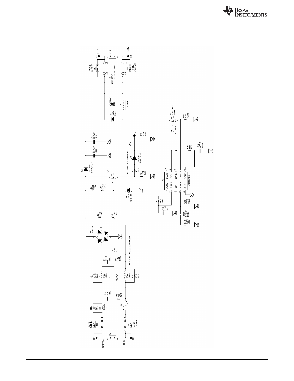
LM3445 Evaluation Board Schematic
5 LM3445 Evaluation Board Schematic
www.ti.com
4
AN-2061 LM3445 A19 Edison Retrofit Evaluation Board SNVA442C–June 2010–Revised May 2013
Copyright © 2010–2013, Texas Instruments Incorporated
Submit Documentation Feedback
Page 5

www.ti.com
Bill of Materials (BOM) LM3445 Evaluation Board
6 Bill of Materials (BOM) LM3445 Evaluation Board
Table 2. Bill of Materials (BOM)
REF DES Description MFG MFG Part Number
U1 IC DRIVER LED W/TRIAC DIM 10VSSOP Texas Instruments LM3445
C1, C10 Ceramic, 47000pF, 500V, X7R, 1210 Johanson Dielectrics 501S41W473KV4E
C2 CAP FILM MKP .0047µF 310VAC X2 Vishay/BC Components BFC233820472
C3 CAP 470µF 50V ELECT PW RADIAL Nichicon UPW1H471MHD
C4/RBLDR
C13, C15 Ceramic, 0.1µF, 16V, X7R, 0603 MuRata GRM188R71C104KA01D
J5, J10 CONN HEADER .312 VERT 2POS TIN Tyco Electronics 1-1318301-2
L1, L2 INDUCTOR 3900µH .12A RADIAL J.W. Miller/Bourns RL875S-392K-RC
R1, R3 RES 200kΩ, 0.25W, 1%, 1206 Vishay-Dale CRCW1206200kFKEA
R2, R7 RES 274kΩ, 0.25W, 1%, 1206 Vishay-Dale CRCW1206274kFKEA
R6, R24 RES 30.1kΩ, 0.25W, 1%, 1206 Vishay-Dale CRCW120630k1FKEA
TP1, TP2, TP3, TP4 Terminal, Turret, TH, Double Keystone Electronics 1502-2
(1)
C4/RBLDR is a dual purpose pad which is unpopulated by default. A ceramic capacitor (C4) may be used here if extra high frequency
bypassing is desired across the LED load. Alternatively a bleeder resistor (RBLDR) in the range of 10kΩ to 100kΩ may be placed here to
quickly discharge C3 and prevent prolonged LED glow due to the energy stored in C3.
(1)
DNP
C5 Ceramic, .33µF, 250V, X7R, 1812 TDK Corporation C4532X7R2E334K
C6 CAP .10µF 305VAC EMI SUPPRESSION EPCOS B32921C3104M
C8 Ceramic, 47µF, X5R, 16V, 1210 MuRata GRM32ER61C476ME15L
C9 Ceramic, .1µF, 250V, X7R, 1210 Taiyo Yuden QMK325B7104KN-T
C12 Ceramic, 470pF, 50V, X7R, 0603 MuRata GRM188R71H471KA01D
C14 Ceramic, 0.47µF, 16V, X7R, 0603 MuRata GRM188R71C474KA88D
D1 DIODE SCHOTTKY 1A 200V PWRDI 123 Diodes Inc. DFLS1200-7
D2 Bridge Rectifier, Vr = 400V, Io = 0.8A, Vf = 1V Diodes Inc. HD04-T
D4 DIODE FAST 1A 300V SMA Fairchild Semi conductor ES1F
D7 DIODE ZENER 15V 500MW SOD-123 Fairchild Semi conductor MMSZ5245B
D8 DIODE SCHOTTKY 1A 200V PWRDI 123 Diodes Inc. DFLS1200-7
F1 FUSE 1A 125V FAST Cooper/Bussman 6125FA1A
L3 820µH, Shielded Drum Core Coilcraft Inc. MSS1038-824KL
M1 JUMPER WIRE 0.3" J6 TO J1 3M 923345-03-C
M2 JUMPER WIRE 0.3" J7 to J4 3M 923345-03-C
M3 JUMPER WIRE 0.3" J2 TO J8 3M 923345-03-C
M4 JUMPER WIRE 0.3" J3 TO J9 3M 923345-03-C
Q1 MOSFET N-CH 240V 260MA SOT-89 Infineon Technologies BSS87 L6327
Q2 MOSFET N-CH 250V 4.4A DPAK Fairchild Semi conductor FDD6N25TM
R4 RES 430Ω, 1/2W, 5%, 2010 Vishay-Dale CRCW2010430RJNEF
R5 RES 430Ω, 1/3W, 5%, 1210 Vishay-Dale CRCW1210430RJNEA
R8 RES 49.9kΩ, 0.1W, 1%, 0603 Vishay-Dale CRCW060349K9FKEA
R9 RES 48.7kΩ, 0.1W, 1%, 0603 Vishay-Dale CRCW060348K7FKEA
R10 DNP
R12 RES 4.7Ω, 0.1W, 5%, 0603 Vishay-Dale CRCW06034R70JNEA
R14 RES 1.54Ω, 1/4W, 1%, 1206 Vishay-Dale CRCW12061R54FNEA
R15 RES 3.16kΩ, 0.1w, 1%, 0603 Vishay-Dale CRCW06033K16FKEA
R16 RES 255kΩ, 0.1W, 1%, 0603 Vishay-Dale CRCW0603255KFKEA
R22 RES 40.2Ω, 0.125W, 1%, 0805 Vishay-Dale CRCW080540R2FKEA
RT1 CURRENT LIMITOR INRUSH 60Ω 20% Cantherm MF72-060D5
SNVA442C–June 2010–Revised May 2013 AN-2061 LM3445 A19 Edison Retrofit Evaluation Board
Submit Documentation Feedback
Copyright © 2010–2013, Texas Instruments Incorporated
5
Page 6

Output Current versus Number of LEDs for Various Modifications
7 Output Current versus Number of LEDs for Various Modifications
www.ti.com
# of LEDs Original Circuit Modification A
Output Current (mA) Output Current (mA) Output Current (mA) Output Current (mA)
(1)
Modification B
(2)
2 520
3 500
4 475
5 340 248 265 455
6 315 235 250 432
7 300 222 237 412
8 275 210 224
9 260 200 212
10 245 190 200
11 230 180 190
12 215 170 180
13 205 164 170
(4)
14
(4)
15
(4)
16
(4)
17
(4)
18
(1)
Modification A: R14 = 2.37Ω, R16 = 150kΩ, C3 = 330µF, 63V.
(2)
Modification B: R14 = 2.2Ω, R16 = 165kΩ.
(3)
Modification C: R14 = 1.2Ω, R16 = 137kΩ, L3 = 470µH, C3 = 1000µF, 25V.
(4)
For all applications using greater than 13 LEDs a 330µF, 63V output capacitor (C3) was used.
196 156 162
190 150 155
183 142 148
175 135 142
170 130 137
Modification C
(3)
6
AN-2061 LM3445 A19 Edison Retrofit Evaluation Board SNVA442C–June 2010–Revised May 2013
Copyright © 2010–2013, Texas Instruments Incorporated
Submit Documentation Feedback
Page 7

LINE VOLTAGE (VAC)
EFFICIENCY (%)
90
85
80
75
70
80 90 100 110 120 130 140
18 LEDs @ 130 mA
LINE VOLTAGE (VAC)
POWER FACTOR
0.95
0.90
0.85
0.80
0.75
80 90 100 110 120 130 140
18 LEDs @ 130 mA
LINE VOLTAGE (VAC)
EFFICIENCY
(%)
90
85
80
75
70
80 90 100 110 120 130 140
9 LEDs @ 260 mA
LINE VOLTAGE (VAC)
POWER FACTOR
0.95
0.90
0.85
0.80
0.75
80 90 100 110 120 130 140
9 LEDs @ 260 mA
www.ti.com
8 Typical Performance Characteristics
Figure 2. Efficiency vs. Line Voltage Figure 3. Power Factor vs. Line Voltage
Original Circuit Original Circuit
Typical Performance Characteristics
SNVA442C–June 2010–Revised May 2013 AN-2061 LM3445 A19 Edison Retrofit Evaluation Board
Submit Documentation Feedback
Figure 4. Efficiency vs. Line Voltage Figure 5. Power Factor vs. Line Voltage
Modification A Modification A
7
Copyright © 2010–2013, Texas Instruments Incorporated
Page 8

LINE VOLTAGE (VAC)
EFFICIENCY
(%)
90
85
80
75
70
80 90 100 110 120 130 140
13 LEDs @ 170 mA
LINE VOLTAGE (VAC)
POWER FACTOR
0.95
0.90
0.85
0.80
0.75
80 90 100 110 120 130 140
13 LEDs @ 170 mA
Typical Performance Characteristics
Figure 6. Efficiency vs. Line Voltage Figure 7. Power Factor vs. Line Voltage
Modification B Modification B
www.ti.com
8
AN-2061 LM3445 A19 Edison Retrofit Evaluation Board SNVA442C–June 2010–Revised May 2013
Copyright © 2010–2013, Texas Instruments Incorporated
Submit Documentation Feedback
Page 9

www.ti.com
9 PCB Layout
PCB Layout
Figure 8. Top Layer
Figure 9. Bottom Layer
WARNING
The LM3445 evaluation boards have no isolation or any type of
protection from shock. Caution must be taken when handling
evaluation board. Avoid touching evaluation board, and removing
any cables while evaluation board is operating. Isolating the
evaluation board rather than the oscilloscope is highly
recommended.
SNVA442C–June 2010–Revised May 2013 AN-2061 LM3445 A19 Edison Retrofit Evaluation Board
Submit Documentation Feedback
Copyright © 2010–2013, Texas Instruments Incorporated
9
Page 10

EMI/EMC Information
10 EMI/EMC Information
www.ti.com
Figure 10. Radiated EMI
10
Figure 11. Conducted EMC. Line = Blue, Neutral = Black
Frequency Amplitude Limit Delta Amplitude Average Limit Delta
Neutral 154 kHz 57 66 -9 47 56 -9
Line 1.1 MHz 31 46 -15
AN-2061 LM3445 A19 Edison Retrofit Evaluation Board SNVA442C–June 2010–Revised May 2013
Quasi-Peak Quasi-Peak Quasi-Peak Average Average
Copyright © 2010–2013, Texas Instruments Incorporated
Submit Documentation Feedback
Page 11

IMPORTANT NOTICE
Texas Instruments Incorporated and its subsidiaries (TI) reserve the right to make corrections, enhancements, improvements and other
changes to its semiconductor products and services per JESD46, latest issue, and to discontinue any product or service per JESD48, latest
issue. Buyers should obtain the latest relevant information before placing orders and should verify that such information is current and
complete. All semiconductor products (also referred to herein as “components”) are sold subject to TI’s terms and conditions of sale
supplied at the time of order acknowledgment.
TI warrants performance of its components to the specifications applicable at the time of sale, in accordance with the warranty in TI’s terms
and conditions of sale of semiconductor products. Testing and other quality control techniques are used to the extent TI deems necessary
to support this warranty. Except where mandated by applicable law, testing of all parameters of each component is not necessarily
performed.
TI assumes no liability for applications assistance or the design of Buyers’ products. Buyers are responsible for their products and
applications using TI components. To minimize the risks associated with Buyers’ products and applications, Buyers should provide
adequate design and operating safeguards.
TI does not warrant or represent that any license, either express or implied, is granted under any patent right, copyright, mask work right, or
other intellectual property right relating to any combination, machine, or process in which TI components or services are used. Information
published by TI regarding third-party products or services does not constitute a license to use such products or services or a warranty or
endorsement thereof. Use of such information may require a license from a third party under the patents or other intellectual property of the
third party, or a license from TI under the patents or other intellectual property of TI.
Reproduction of significant portions of TI information in TI data books or data sheets is permissible only if reproduction is without alteration
and is accompanied by all associated warranties, conditions, limitations, and notices. TI is not responsible or liable for such altered
documentation. Information of third parties may be subject to additional restrictions.
Resale of TI components or services with statements different from or beyond the parameters stated by TI for that component or service
voids all express and any implied warranties for the associated TI component or service and is an unfair and deceptive business practice.
TI is not responsible or liable for any such statements.
Buyer acknowledges and agrees that it is solely responsible for compliance with all legal, regulatory and safety-related requirements
concerning its products, and any use of TI components in its applications, notwithstanding any applications-related information or support
that may be provided by TI. Buyer represents and agrees that it has all the necessary expertise to create and implement safeguards which
anticipate dangerous consequences of failures, monitor failures and their consequences, lessen the likelihood of failures that might cause
harm and take appropriate remedial actions. Buyer will fully indemnify TI and its representatives against any damages arising out of the use
of any TI components in safety-critical applications.
In some cases, TI components may be promoted specifically to facilitate safety-related applications. With such components, TI’s goal is to
help enable customers to design and create their own end-product solutions that meet applicable functional safety standards and
requirements. Nonetheless, such components are subject to these terms.
No TI components are authorized for use in FDA Class III (or similar life-critical medical equipment) unless authorized officers of the parties
have executed a special agreement specifically governing such use.
Only those TI components which TI has specifically designated as military grade or “enhanced plastic” are designed and intended for use in
military/aerospace applications or environments. Buyer acknowledges and agrees that any military or aerospace use of TI components
which have not been so designated is solely at the Buyer's risk, and that Buyer is solely responsible for compliance with all legal and
regulatory requirements in connection with such use.
TI has specifically designated certain components as meeting ISO/TS16949 requirements, mainly for automotive use. In any case of use of
non-designated products, TI will not be responsible for any failure to meet ISO/TS16949.
Products Applications
Audio www.ti.com/audio Automotive and Transportation www.ti.com/automotive
Amplifiers amplifier.ti.com Communications and Telecom www.ti.com/communications
Data Converters dataconverter.ti.com Computers and Peripherals www.ti.com/computers
DLP® Products www.dlp.com Consumer Electronics www.ti.com/consumer-apps
DSP dsp.ti.com Energy and Lighting www.ti.com/energy
Clocks and Timers www.ti.com/clocks Industrial www.ti.com/industrial
Interface interface.ti.com Medical www.ti.com/medical
Logic logic.ti.com Security www.ti.com/security
Power Mgmt power.ti.com Space, Avionics and Defense www.ti.com/space-avionics-defense
Microcontrollers microcontroller.ti.com Video and Imaging www.ti.com/video
RFID www.ti-rfid.com
OMAP Applications Processors www.ti.com/omap TI E2E Community e2e.ti.com
Wireless Connectivity www.ti.com/wirelessconnectivity
Mailing Address: Texas Instruments, Post Office Box 655303, Dallas, Texas 75265
Copyright © 2013, Texas Instruments Incorporated
 Loading...