

Page 1

Application Report
SNVA429C–August 2010–Revised May 2013
AN-2034 LM3445 -120VAC, 8W Isolated Flyback
LED Driver
.....................................................................................................................................................
ABSTRACT
This demonstration board highlights the performance of a LM3445 based Flyback LED driver solution that
can be used to power a single LED string consisting of 4 to 8 series connected LEDs from an 90 V
135 V
, 60 Hz input power supply. The key performance characteristics under typical operating
RMS
conditions are summarized in this application report.
Contents
1 Introduction .................................................................................................................. 3
2 Key Features ................................................................................................................ 3
3 Applications .................................................................................................................. 3
4 Performance Specifications ................................................................................................ 3
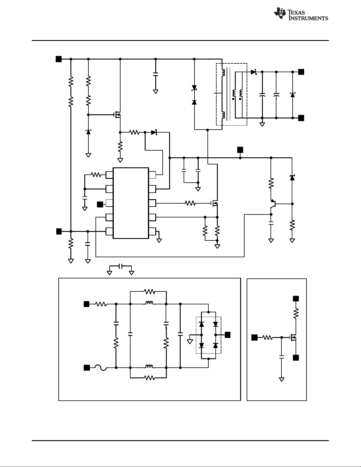
5 LM3445 120VAC, 8W Isolated Flyback LED Driver Demo Board Schematic ...................................... 5
6 LM3445 Device Pin-Out .................................................................................................... 7
7 Bill of Materials .............................................................................................................. 7
8 Demo Board Wiring Overview ............................................................................................. 9
9 Demo Board Assembly ................................................................................................... 10
10 Typical Performance Characteristics .................................................................................... 11
11 PCB Layout ................................................................................................................. 14
12 Transformer Design ....................................................................................................... 15
13 Experimental Results ..................................................................................................... 16
13.1 Non-Dimming Performance ..................................................................................... 16
13.2 Dimming Performance ........................................................................................... 17
13.3 Power Factor Performance ...................................................................................... 19
14 Circuit Operation With Rotary Forward Phase TRIAC Dimmer ..................................................... 20
15 Circuit Operation With Reverse Phase TRIAC Dimmer .............................................................. 21
16 Electromagnetic Interference (EMI) ..................................................................................... 22
17 Thermal Analysis .......................................................................................................... 24
18 Circuit Analysis and Explanations ....................................................................................... 26
18.1 Injecting Line Voltage into Filter-2 (Achieving PFC > 0.95) ................................................. 26
RMS
to
List of Figures
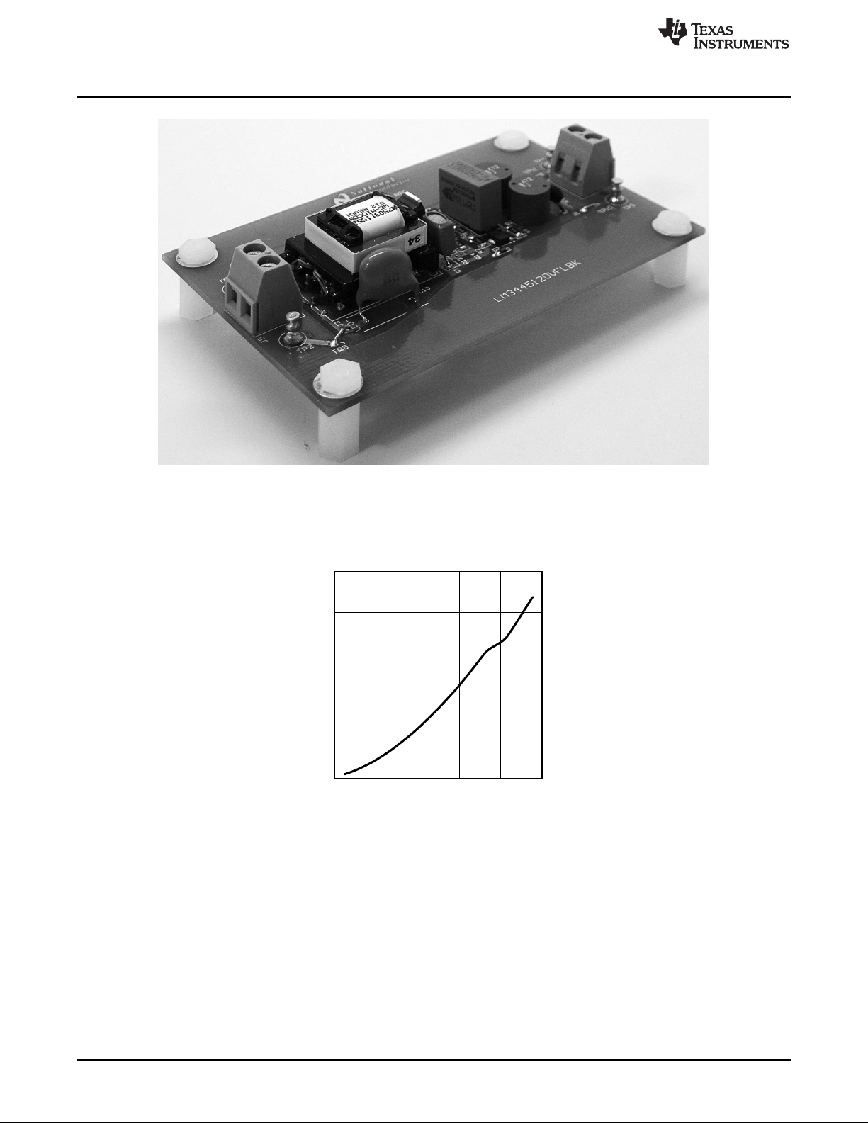
1 Demo Board ................................................................................................................. 4
2 LED Current vs. Input Voltage (using Dimmer)......................................................................... 4
3 Demo Board Schematic.................................................................................................... 6
4 LM3445 Device Pin-Out.................................................................................................... 7
5 Wiring Connection Diagram ............................................................................................... 9
6 Top View.................................................................................................................... 10
7 Bottom View................................................................................................................ 10
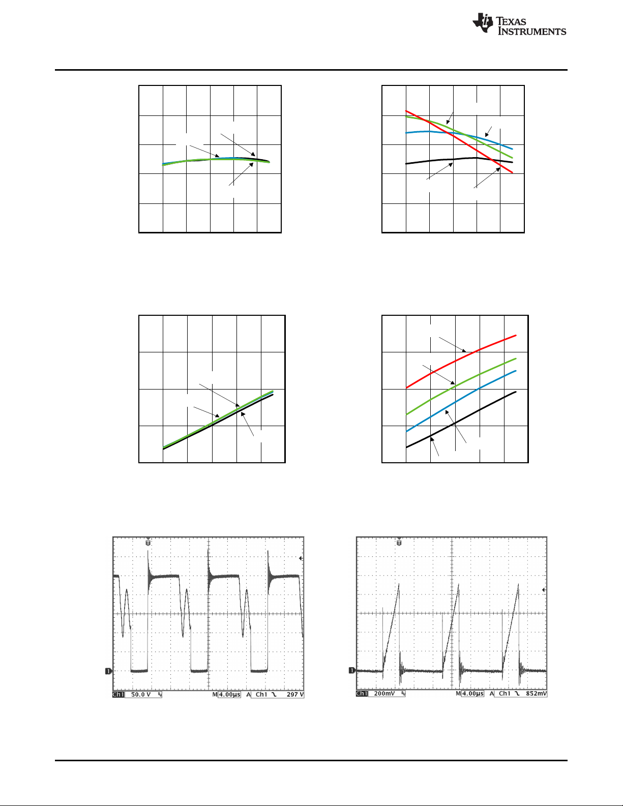
8 Efficiency vs. Line Voltage Original Circuit............................................................................. 11
9 Efficiency vs. Line Voltage Modified Circuits .......................................................................... 11
10 LED Current vs. Line Voltage Original Circuit ......................................................................... 11
PowerWise is a trademark of Texas Instruments.
All other trademarks are the property of their respective owners.
SNVA429C–August 2010–Revised May 2013 AN-2034 LM3445 -120VAC, 8W Isolated Flyback LED Driver
Submit Documentation Feedback
Copyright © 2010–2013, Texas Instruments Incorporated
1
Page 2

www.ti.com
11 LED Current vs. Line Voltage Modified Circuits....................................................................... 11
12 Power Factor vs. Line Voltage Original Circuit ........................................................................ 11
13 Power Factor vs. Line Voltage Modified Circuits...................................................................... 11
14 Output Power vs. Line Voltage Original Circuit........................................................................ 12
15 Output Power vs. Line Voltage Modified Circuits ..................................................................... 12
16 Power MOSFET Drain Voltage Waveform (VIN= 120V
17 Current Sense Waveform (VIN= 120V
18 FLTR2 Waveform (VIN= 120V
, 6 LEDs, I
RMS
, 6 LEDs, I
RMS
LED
= 350mA) ........................................................... 12
, 6 LEDs, I
RMS
= 350mA) .................................................. 12
LED
= 350mA)............................... 12
LED
19 Top Layer................................................................................................................... 14
20 Bottom Layer............................................................................................................... 14
21 LED Current vs. Input Voltage (using Dimmer) ....................................................................... 18
22 Current Harmonic Performance vs. EN/IEC61000-3-2 Class C Limits............................................. 19
23 Forward Phase Circuit at Full Brightness .............................................................................. 20
24 Forward Phase Circuit at 90° Firing Angle............................................................................. 20
25 Forward Phase Circuit at 150° Firing Angle ........................................................................... 20
26 Reverse Phase Circuit at Full Brightness .............................................................................. 21
27 Reverse Phase Circuit at 90° Firing Angle............................................................................. 21
28 Reverse Phase Circuit at 150° Firing Angle ........................................................................... 21
29 Input EMI Filter and Rectifier Circuit.................................................................................... 22
30 Peak Conductive EMI Scan per CISPR-22, Class B Limits.......................................................... 22
31 Peak Conductive EMI Scan with Additional 33nF of Input Capacitance........................................... 23
32 Top Side Thermal Scan .................................................................................................. 24
33 Bottom Side Thermal Scan............................................................................................... 25
34 Line Voltage Injection Circuit............................................................................................. 26
35 FLTR2 Waveform with No Dimmer ..................................................................................... 26
36 Typical Operation of FLTR2 Pin ........................................................................................ 27
List of Tables
1 Pin Description 10 Pin VSSOP............................................................................................ 7
2 Wiring Connection .......................................................................................................... 9
3 Measured Efficiency and Line Regulation (6 LEDs, No TRIAC Dimmer).......................................... 16
4 LED Current, Output Power Versus Number of LEDs for Various Circuit Modifications (VIN= 120 VAC, no
TRIAC Dimmer)............................................................................................................ 16
5 Measured Efficiency and Line Regulation Data (with TRIAC Dimmer)............................................. 17
2
AN-2034 LM3445 -120VAC, 8W Isolated Flyback LED Driver SNVA429C–August 2010–Revised May 2013
Copyright © 2010–2013, Texas Instruments Incorporated
Submit Documentation Feedback
Page 3

www.ti.com
1 Introduction
This is a two-layer board using the bottom and top layer for component placement. The demonstration
board can be modified to adjust the LED forward current, the number of series connected LEDs that are
driven and the switching frequency. For detailed instructions, see Triac Dimmable Offline LED Driver
(SNVS570).
A bill of materials is included that describes the parts used on this demonstration board. A schematic and
layout have also been included along with measured performance characteristics.
2 Key Features
• Drop-in compatibility with TRIAC dimmers
• Line injection circuitry enables PFC values greater than 0.95
• Adjustable LED current and switching frequency
• Flicker free operation
3 Applications
• Retro-fit TRIAC Dimming
• Solid State Lighting
• Industrial and Commercial Lighting
• Residential Lighting
Introduction
4 Performance Specifications
Based on an LED Vf= 3.4V
Symbol Parameter Min Typ Max
V
IN
V
OUT
I
LED
P
OUT
f
sw
Input voltage 90 V
LED string voltage 13 V 20 V 27 V
LED string average current - 365 mA -
Output power - 7.3 W -
Switching frequency - 78.5 kHz -
RMS
120 V
RMS
135 V
RMS
SNVA429C–August 2010–Revised May 2013 AN-2034 LM3445 -120VAC, 8W Isolated Flyback LED Driver
Submit Documentation Feedback
Copyright © 2010–2013, Texas Instruments Incorporated
3
Page 4
Input Voltage (V
rms
)
I
LED
(mA)
400
320
240
160
80
0
10 32 54 76 98 120
Performance Specifications
www.ti.com
Figure 1. Demo Board
4
AN-2034 LM3445 -120VAC, 8W Isolated Flyback LED Driver SNVA429C–August 2010–Revised May 2013
Figure 2. LED Current vs. Input Voltage (using Dimmer)
Copyright © 2010–2013, Texas Instruments Incorporated
Submit Documentation Feedback
Page 5

www.ti.com
LM3445 120VAC, 8W Isolated Flyback LED Driver Demo Board Schematic
5 LM3445 120VAC, 8W Isolated Flyback LED Driver Demo Board Schematic
WARNING
The LM3445 evaluation board has exposed high voltage
components that present a shock hazard. Care must be taken when
handling the evaluation board. Avoid touching the evaluation
board and removing any cables while the evaluation board is
operating. Isolating the evaluation board rather than the
oscilloscope is highly recommended.
CAUTION
The ground connection on the evaluation board is NOT referenced to earth
ground. If an oscilloscope ground lead is connected to the evaluation board
ground test point for analysis and AC power is applied, the fuse (F1) will fail
open. The oscilloscope should be powered via an isolation transformer before
an oscilloscope ground lead is connected to the evaluation board.
The LM3445 evaluation board should not be powered with an open load. For
proper operation, ensure that the desired number of LEDs are connected at the
output before applying power to the evaluation board.
SNVA429C–August 2010–Revised May 2013 AN-2034 LM3445 -120VAC, 8W Isolated Flyback LED Driver
Submit Documentation Feedback
Copyright © 2010–2013, Texas Instruments Incorporated
5
Page 6
R15
C11
FLTR2
R2
R7
DIM
R9
C14
R1
R3
D7
Q1
R8
ASNS
FLTR1
DIM
COFF
FLTR2
BLDR
VCC
GND
GATE
ISNS
LM3445
1
2
3
4
5
10
9
8
7
6
V+
C7 C8
V
CC
R22 D8
R12
R13 R14
+
VLED+
VLED±
L1
C5
R4
V+
LINE
NEUTRAL
INPUT EMI FILTER AND RECTIFIER CIRCUIT
Q2
D1
D3
D4
D5C3
C4
DIM
V
CC
FLTR2
R11
C10
R10
TRIAC HOLDING
CIRCUIT
R16
C12
Q3
Q4
R20
C1
D6
C6
L2
R6
R24
C9
R5
C2
RT1
D2
F1
T1
C13
+
LM3445 120VAC, 8W Isolated Flyback LED Driver Demo Board Schematic
www.ti.com
6
AN-2034 LM3445 -120VAC, 8W Isolated Flyback LED Driver SNVA429C–August 2010–Revised May 2013
Figure 3. Demo Board Schematic
Copyright © 2010–2013, Texas Instruments Incorporated
Submit Documentation Feedback
Page 7
1
4
3
2
10
7
8
9
I
SNS
FLTR1
GATE
BLDR
COFF
V
CC
ASNS
DIM
5 6FLTR2 GND
www.ti.com
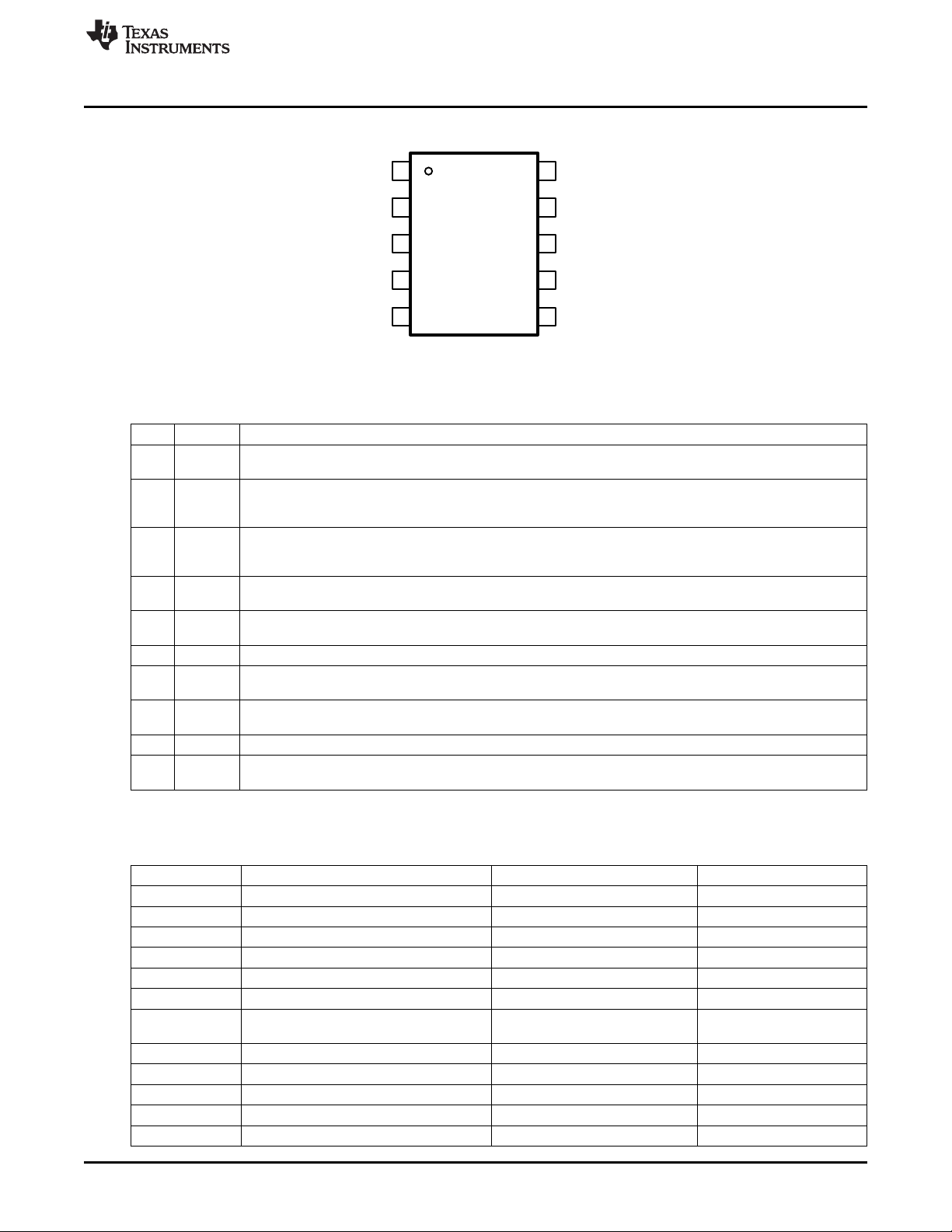
6 LM3445 Device Pin-Out
Pin # Name Description
1 ASNS PWM output of the TRIAC dimmer decoder circuit. Outputs a 0 to 4V PWM signal with a duty cycle proportional
2 FLTR1 First filter input. The 120Hz PWM signal from ASNS is filtered to a DC signal and compared to a 1 to 3V, 5.85
3 DIM Input/output dual function dim pin. This pin can be driven with an external PWM signal to dim the LEDs. It may
4 COFF OFF time setting pin. A user set current and capacitor connected from the output to this pin sets the constant
5 FLTR2 Second filter input. A capacitor tied to this pin filters the PWM dimming signal to supply a DC voltage to control
6 GND Circuit ground connection.
7 ISNS LED current sense pin. Connect a resistor from main switching MOSFET source, ISNS to GND to set the
8 GATE Power MOSFET driver pin. This output provides the gate drive for the power switching MOSFET of the buck
9 V
10 BLDR Bleeder pin. Provides the input signal to the angle detect circuitry as well as a current path through a switched
to the TRIAC dimmer on-time.
kHz ramp to generate a higher frequency PWM signal with a duty cycle proportional to the TRIAC dimmer firing
angle. Pull above 4.9V (typical) to tri-state DIM.
also be used as an output signal and connected to the DIM pin of other LM3445 or LED drivers to dim multiple
LED circuits simultaneously.
OFF time of the switching controller.
the LED current. Could also be used as an analog dimming input.
maximum LED current.
controller.
Input voltage pin. This pin provides the power for the internal control circuitry and gate driver.
CC
230Ω resistor to ensure proper firing of the TRIAC dimmer.
LM3445 Device Pin-Out
Figure 4. LM3445 Device Pin-Out
Table 1. Pin Description 10 Pin VSSOP
7 Bill of Materials
Designator Description Manufacturer Part Number
AA1 Printed Circuit Board - 551600457-001A
C1 CAP .047UF 630V METAL POLYPRO EPCOS Inc B32559C6473K000
C2 CAP 10000PF X7R 250VAC X2 2220 Murata Electronics North America GA355DR7GB103KY02L
C3, C4 CAP 330UF 35V ELECT PW Nichicon UPW1V331MPD6
C5 CAP CER .33UF 250V X7R 1812 TDK Corporation C4532X7R2E334K
C6 CAP .10UF 305VAC EMI SUPPRESSION EPCOS B32921C3104M
C7 CAP, CERM, 0.1µF, 16V, +/-10%, X7R, Kemet C0805C104K4RACTU
SNVA429C–August 2010–Revised May 2013 AN-2034 LM3445 -120VAC, 8W Isolated Flyback LED Driver
Submit Documentation Feedback
C8 CAP CER 47UF 16V X5R 1210 MuRata GRM32ER61C476ME15L
C9 CAP CER .10UF 250V X7R 10% 1206 TDK C3216X7R2E104K
C10 CAP CER .22UF 16V X7R 0603 MuRata GRM188R71C224KA01D
C11 CAP CER 2200PF 50V 10% X7R 0603 MuRata GRM188R71H222KA01D
C12 CAP CER 330PF 50V 5% C0G 0603 MuRata GRM1885C1H331JA01D
0805
Copyright © 2010–2013, Texas Instruments Incorporated
7
Page 8

Bill of Materials
Designator Description Manufacturer Part Number
J1, J2, J3, J4, 16 GA WIRE HOLE, 18 GA WIRE HOLE 3M 923345-02-C
TP8, TP9, TP10
R1, R3 RES 200K OHM 1/4W 5% 1206 SMD Vishay-Dale CRCW1206200KJNEA
R2, R7 RES, 309k ohm, 1%, 0.25W, 1206 Vishay-Dale CRCW1206309KFKEA
R4, R5 RES, 430 ohm, 5%, 0.25W, 1206 Vishay-Dale CRCW1206430RJNEA
R6, R24 RES, 10.5k ohm, 1%, 0.125W, 0805 Vishay-Dale CRCW080510K5FKEA
R8, R11 RES 49.9K OHM 1/10W 1% 0603 SMD Vishay-Dale CRCW060349K9FKEA
TP2-TP5 Terminal, Turret, TH, Double Keystone Electronics 1502-2
www.ti.com
C13 CAP CER 2200PF 250VAC X1Y1 RAD TDK Corporation CD12-E2GA222MYNS
C14 CAP CERM .47UF 10% 25V X5R 0805 AVX 08053D474KAT2A
D1 DIODE TVS 150V 600W UNI 5% SMB Littlefuse SMAJ120A
D2 RECT BRIDGE GP 600V 0.5A MINIDIP Diodes Inc. RH06-T
D3 DIODE RECT GP 1A 1000V MINI-SMA Comchip Technology CGRM4007-G
D4 DIODE SCHOTTKY 100V 1A SMA ST Microelectronics STPS1H100A
D5 DIODE ZENER 30V 1.5W SMA ON Semiconductor 1SMA5936BT3G
D6 DIODE ZENER 5.1V 200MW SOD-523F Fairchild Semiconductor MM5Z5V1
D7 DIODE ZENER 12V 200MW Fairchild Semiconductor MM5Z12V
D8 DIODE SWITCH 200V 200MW Diode Inc BAV20WS-7-F
F1 FUSE BRICK 1A 125V FAST 6125FA Cooper/Bussmann 6125FA
J5, J6 Conn Term Block, 2POS, 5.08mm PCB Phoenix Contact 1715721
L1, L2 INDUCTOR 4700UH .13A RADIAL TDK Corporation TSL0808RA-472JR13-PF
Q1 MOSFET N-CH 600V 90MA SOT-89 Infineon Technologies BSS225 L6327
Q2 MOSFET N-CH 600V 1.8A TO-251 Infineon Technology SPU02N60S5
Q3 MOSFET N-CH 100V 170MA SC70-3 Diodes Inc BSS123W-7-F
Q4 TRANS GP SS PNP 40V SOT323 On Semiconductor MMBT3906WT1G
R9 RES 100K OHM 1/10W 1% 0603 SMD Vishay-Dale CRCW0603100KFKEA
R10 DNP - R12 RES 4.7 OHM 1/10W 5% 0603 SMD Vishay-Dale CRCW06034R70JNEA
R13 RES 10 OHM 1/8W 5% 0805 SMD Vishay-Dale CRCW080510R0JNEA
R14 RES 1.50 OHM 1/4W 1% 1206 SMD Vishay-Dale CRCW12061R50FNEA
R15 RES 3.48K OHM 1/10W 1% 0603 SMD Vishay-Dale CRCW06033K48FKEA
R16 RES 75.0K OHM 1/10W 1% 0603 SMD Vishay-Dale CRCW060375K0FKEA
R20 RES 30.1K OHM 1/10W 1% 0603 SMD Vishay-Dale CRCW060330K1FKEA
R22 RES 40.2 OHM 1/8W 1% 0805 SMD Vishay-Dale CRCW080540R2FKEA
RT1 CURRENT LIMITOR INRUSH 60OHM Cantherm MF72-060D5
20%
T1 Transformer Wurth Electronics 750311553 Rev. 01
TP7 TEST POINT ICT - -
U1 TRIAC Dimmable Offline LED Driver, Texas Instruments LM3445
PowerWise™
8
AN-2034 LM3445 -120VAC, 8W Isolated Flyback LED Driver SNVA429C–August 2010–Revised May 2013
Copyright © 2010–2013, Texas Instruments Incorporated
Submit Documentation Feedback
Page 9

LED +
LED -
LINE
NEUTRAL
J5
J6
TP3
TP2
TP4
TP5
www.ti.com
8 Demo Board Wiring Overview
Figure 5. Wiring Connection Diagram
Test Name I/O Description
Point
TP3 LED + Output LED Constant Current Supply
TP2 LED - Output LED Return Connection (not GND)
TP4 LINE Input AC Line Voltage
TP5 NEUTRAL Input AC Neutral
Demo Board Wiring Overview
Table 2. Wiring Connection
Supplies voltage and constant-current to anode of LED string.
Connects to cathode of LED string. Do NOT connect to GND.
Connects directly to AC line or output of TRIAC dimmer of a 120VAC system.
Connects directly to AC neutral of a 120VAC system.
SNVA429C–August 2010–Revised May 2013 AN-2034 LM3445 -120VAC, 8W Isolated Flyback LED Driver
Submit Documentation Feedback
Copyright © 2010–2013, Texas Instruments Incorporated
9
Page 10
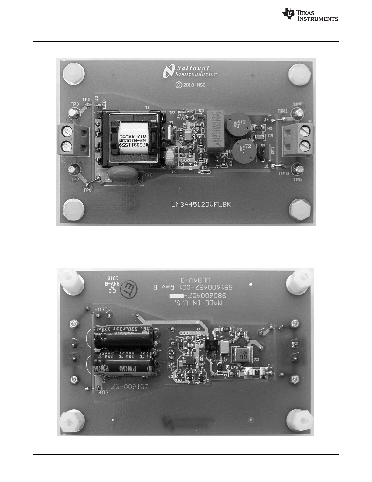
Demo Board Assembly
9 Demo Board Assembly
www.ti.com
Figure 6. Top View
10
Figure 7. Bottom View
AN-2034 LM3445 -120VAC, 8W Isolated Flyback LED Driver SNVA429C–August 2010–Revised May 2013
Copyright © 2010–2013, Texas Instruments Incorporated
Submit Documentation Feedback
Page 11

80 90 100 110 120 130 140
0.0
0.2
0.4
0.7
0.8
1.0
I
LED
(A)
LINE VOLTAGE (V
RMS
)
4 LEDs
6 LEDs
8 LEDs
80 90 100 110 120 130 140
0.0
0.2
0.4
0.7
0.8
1.0
I
LED
(A)
LINE VOLTAGE (V
RMS
)
Original
Mod A
Mod B
Mod C
80 90 100 110 120 130 140
72
74
76
78
80
82
EFFICIENCY (%)
LINE VOLTAGE (V
RMS
)
4 LEDs
6 LEDs
8 LEDs
80 90 100 110 120 130 140
72
74
76
78
80
82
EFFICIENCY (%)
LINE VOLTAGE (V
RMS
)
Mod C
Mod A
Mod B
Original
www.ti.com
10 Typical Performance Characteristics
Original Circuit: R14 = 1.50Ω; Modification A: R14 = 1.20Ω; Modification B: R14 = 1.00Ω; Modification C:
R14 = 0.75Ω
Figure 8. Efficiency vs. Line Voltage Figure 9. Efficiency vs. Line Voltage
Original Circuit Modified Circuits
Typical Performance Characteristics
Figure 10. LED Current vs. Line Voltage Figure 11. LED Current vs. Line Voltage
Original Circuit Modified Circuits
Copyright © 2010–2013, Texas Instruments Incorporated
SNVA429C–August 2010–Revised May 2013 AN-2034 LM3445 -120VAC, 8W Isolated Flyback LED Driver
Submit Documentation Feedback
11
Page 12
80 90 100 110 120 130 140
3
6
9
12
15
P
OUT
(W)
LINE VOLTAGE (V
RMS
)
4 LEDs
6 LEDs
8 LEDs
80 90 100 110 120 130 140
3
6
9
12
15
P
OUT
(W)
LINE VOLTAGE (V
RMS
)
Original
Mod A
Mod B
Mod C
80 90 100 110 120 130 140
90
92
94
96
98
100
POWER FACTOR
LINE VOLTAGE (V
RMS
)
4 LEDs
8 LEDs
6 LEDs
80 90 100 110 120 130 140
90
92
94
96
98
100
POWER FACTOR
LINE VOLTAGE (V
RMS
)
Original
Mod A
Mod B
Mod C
Typical Performance Characteristics
Figure 12. Power Factor vs. Line Voltage Figure 13. Power Factor vs. Line Voltage
Original Circuit Modified Circuits
www.ti.com
Figure 14. Output Power vs. Line Voltage Figure 15. Output Power vs. Line Voltage
(VIN= 120V
Figure 16. Power MOSFET Drain Voltage Waveform Figure 17. Current Sense Waveform
12
AN-2034 LM3445 -120VAC, 8W Isolated Flyback LED Driver SNVA429C–August 2010–Revised May 2013
Original Circuit Modified Circuits
RMS
, 6 LEDs, I
= 350mA) (VIN= 120V
LED
Copyright © 2010–2013, Texas Instruments Incorporated
, 6 LEDs, I
RMS
Submit Documentation Feedback
= 350mA)
LED
Page 13

www.ti.com
Figure 18. FLTR2 Waveform
(VIN= 120V
, 6 LEDs, I
RMS
= 350mA)
LED
Typical Performance Characteristics
SNVA429C–August 2010–Revised May 2013 AN-2034 LM3445 -120VAC, 8W Isolated Flyback LED Driver
Submit Documentation Feedback
Copyright © 2010–2013, Texas Instruments Incorporated
13
Page 14

PCB Layout
11 PCB Layout
www.ti.com
Figure 19. Top Layer
14
Figure 20. Bottom Layer
AN-2034 LM3445 -120VAC, 8W Isolated Flyback LED Driver SNVA429C–August 2010–Revised May 2013
Copyright © 2010–2013, Texas Instruments Incorporated
Submit Documentation Feedback
Page 15

www.ti.com
12 Transformer Design
Mfg: Wurth Electronics, Part #: 750311553 Rev. 01
Transformer Design
SNVA429C–August 2010–Revised May 2013 AN-2034 LM3445 -120VAC, 8W Isolated Flyback LED Driver
Submit Documentation Feedback
Copyright © 2010–2013, Texas Instruments Incorporated
15
Page 16

Experimental Results
13 Experimental Results
The LED driver is designed to accurately emulate an incandescent light bulb and therefore behave as an
emulated resistor. The resistor value is determined based on the LED string configuration and the desired
output power. The circuit then operates in open-loop, with a fixed duty cycle based on a constant on-time
and constant off-time that is set by selecting appropriate circuit components. Like an incandescent lamp,
the driver is compatible with both forward and reverse phase dimmers.
13.1 Non-Dimming Performance
In steady state, the LED string voltage is measured to be 20.1 V and the average LED current is
measured as 365 mA. The 120 Hz current ripple flowing through the LED string was measured to be 182
mA
connected across the output port and the TRIAC firing angle. The ripple current can be reduced by
increasing the value of energy storage capacitor or by increasing the LED string voltage. With TRIAC
dimmers, the ripple magnitude is directly proportional to the input power and therefore reduces at lower
LED current.
The LED driver switching frequency is measured to be close to the specified 78.5 kHz. The circuit
operates with a constant duty cycle of 0.28 and consumes near 9.2 W of input power. The driver steady
state performance for an LED string consisting of 6 series LEDs without using a TRIAC dimmer is
summarized in Table 3.
at full load. The magnitude of the ripple is a function of the value of energy storage capacitors
pk-pk
Table 3. Measured Efficiency and Line Regulation (6 LEDs, No TRIAC Dimmer)
VIN(V
) IIN(mA
RMS
) PIN(W) V
RMS
89.98 64 5.44 19.24 222 4.27 78.5 94.7
95.03 67 6.03 19.40 244 4.73 78.5 94.8
100.00 70 6.62 19.55 267 5.22 78.8 94.9
104.97 73 7.24 19.69 291 5.73 79.1 95.0
110.03 76 7.90 19.83 315 6.25 79.1 95.0
115.00 78 8.55 19.95 340 6.78 79.3 95.1
120.05 81 9.21 20.06 365 7.32 79.5 95.1
125.02 83 9.84 20.14 389 7.83 79.6 95.0
129.99 85 10.44 20.22 412 8.33 79.8 94.9
135.04 86 11.02 20.29 433 8.79 79.7 94.8
(V) I
OUT
(mA) P
LED
www.ti.com
(W) Efficiency (%) Power Factor
OUT
16
Table 4. LED Current, Output Power Versus Number of LEDs for Various Circuit Modifications
(VIN= 120 VAC, no TRIAC Dimmer)
# of LEDs Original Circuit
I
(mA) P
LED
(1)
(W) I
OUT
Modification A
(mA) P
LED
4 513 7.11 627 8.83 683 10.03 805 11.91
6 365 7.32 435 9.09 481 10.22 566 12.23
8 276 7.34 334 9.16 367 10.16 431 12.12
(1)
Original Circuit: R14 = 1.50Ω; Modification A: R14 = 1.20Ω; Modification B: R14 = 1.00Ω; Modification C: R14 = 0.75Ω
AN-2034 LM3445 -120VAC, 8W Isolated Flyback LED Driver SNVA429C–August 2010–Revised May 2013
Copyright © 2010–2013, Texas Instruments Incorporated
(1)
(W) I
OUT
Modification B
(mA) P
LED
(1)
(W) I
OUT
Modification C
(mA) P
LED
Submit Documentation Feedback
OUT
(1)
(W)
Page 17

www.ti.com
13.2 Dimming Performance
The LED driver is capable of matching or exceeding the dimming performance of an incandescent lamp.
Using a simple rotary TRIAC dimmer, smooth and near logarithmic dimming performance is achieved. By
varying the firing angle of the TRIAC dimmer and measuring the corresponding input and output
parameters, the dimming performance of the demonstration board driving 6 LEDs is summarized in
Table 5.
Table 5. Measured Efficiency and Line Regulation Data (with TRIAC Dimmer)
VIN(V
) VO(V) IO(mA) P
RMS
115.0 19.9 351 7.0
110.1 19.8 323 6.4
105.2 19.7 295 5.8
100.4 19.6 269 5.3
95.5 19.6 258 5.0
90.7 19.5 248 4.8
85.2 19.4 222 4.3
80.2 19.3 199 3.8
75.1 19.2 176 3.4
70.8 19.1 159 3.0
65.5 18.7 138 2.6
60.5 18.8 120 2.3
55.2 18.6 101 1.9
50.6 18.5 86 1.6
45.7 18.3 72 1.3
39.4 18.0 54 1.0
34.2 17.8 42 0.7
30.3 17.6 33 0.6
26.0 17.4 25 0.4
20.0 17.0 15 0.3
15.2 16.6 9 0.1
Experimental Results
(W)
OUT
SNVA429C–August 2010–Revised May 2013 AN-2034 LM3445 -120VAC, 8W Isolated Flyback LED Driver
Submit Documentation Feedback
Copyright © 2010–2013, Texas Instruments Incorporated
17
Page 18

Input Voltage (V
rms
)
I
LED
(mA)
400
320
240
160
80
0
10 32 54 76 98 120
Experimental Results
www.ti.com
Figure 21. LED Current vs. Input Voltage (using Dimmer)
18
AN-2034 LM3445 -120VAC, 8W Isolated Flyback LED Driver SNVA429C–August 2010–Revised May 2013
Copyright © 2010–2013, Texas Instruments Incorporated
Submit Documentation Feedback
Page 19

www.ti.com
13.3 Power Factor Performance
The LED driver is able to achieve close to unity power factor (P.F. ~ 0.95) which meets Energy Star
requirements. This design also exhibits low current harmonics as a percentage of the fundamental current
(as shown in the following figure) and therefore meets the requirements of the IEC 61000-3-2 Class-3
standard.
Experimental Results
Figure 22. Current Harmonic Performance vs. EN/IEC61000-3-2 Class C Limits
SNVA429C–August 2010–Revised May 2013 AN-2034 LM3445 -120VAC, 8W Isolated Flyback LED Driver
Submit Documentation Feedback
Copyright © 2010–2013, Texas Instruments Incorporated
19
Page 20

Circuit Operation With Rotary Forward Phase TRIAC Dimmer
14 Circuit Operation With Rotary Forward Phase TRIAC Dimmer
The dimming operation of the circuit was verified using a forward phase rotary TRIAC dimmer. Waveforms
captured at different dimmer settings are shown in the following figures.
www.ti.com
Figure 23. Forward Phase Circuit at Full Brightness Figure 24. Forward Phase Circuit at 90° Firing Angle
Figure 25. Forward Phase Circuit at 150° Firing Angle
20
AN-2034 LM3445 -120VAC, 8W Isolated Flyback LED Driver SNVA429C–August 2010–Revised May 2013
Copyright © 2010–2013, Texas Instruments Incorporated
Submit Documentation Feedback
Page 21

www.ti.com
Circuit Operation With Reverse Phase TRIAC Dimmer
15 Circuit Operation With Reverse Phase TRIAC Dimmer
The circuit operation was also verified using a reverse phase dimmer and waveforms captured at different
dimmer settings are shown in the following figures.
Figure 26. Reverse Phase Circuit at Full Brightness Figure 27. Reverse Phase Circuit at 90° Firing Angle
Figure 28. Reverse Phase Circuit at 150° Firing Angle
SNVA429C–August 2010–Revised May 2013 AN-2034 LM3445 -120VAC, 8W Isolated Flyback LED Driver
Submit Documentation Feedback
Copyright © 2010–2013, Texas Instruments Incorporated
21
Page 22

L1
C5
R4
V+
LINE
NEUTRAL
C6
L2
R6
R24
C9
R5
C2
RT1
D2
F1
Electromagnetic Interference (EMI)
16 Electromagnetic Interference (EMI)
The EMI input filter of this evaluation board is configured as shown in Figure 29.
Figure 29. Input EMI Filter and Rectifier Circuit
www.ti.com
In order to get a quick estimate of the EMI filter performance, only the PEAK conductive EMI scan was
measured and the data was compared to the Class B conducted EMI limits published in FCC – 47,
section 15.
Figure 30. Peak Conductive EMI Scan per CISPR-22, Class B Limits
If an additional 33nF of input capacitance (that is, C6) is utilized in the input filter, the EMI conductive
performance is further improved as shown in Figure 31.
22
AN-2034 LM3445 -120VAC, 8W Isolated Flyback LED Driver SNVA429C–August 2010–Revised May 2013
Copyright © 2010–2013, Texas Instruments Incorporated
Submit Documentation Feedback
Page 23

www.ti.com
Electromagnetic Interference (EMI)
Figure 31. Peak Conductive EMI Scan with Additional 33nF of Input Capacitance
SNVA429C–August 2010–Revised May 2013 AN-2034 LM3445 -120VAC, 8W Isolated Flyback LED Driver
Submit Documentation Feedback
Copyright © 2010–2013, Texas Instruments Incorporated
23
Page 24

Thermal Analysis
17 Thermal Analysis
The board temperature was measured using an IR camera (HIS-3000, Wahl) while running under the
following conditions:
• VIN= 120 V
• I
= 365 mA
LED
• Number of LEDs = 6
• P
OUT
The results are shown in the following figures.
RMS
= 7.3 W
www.ti.com
24
Figure 32. Top Side Thermal Scan
AN-2034 LM3445 -120VAC, 8W Isolated Flyback LED Driver SNVA429C–August 2010–Revised May 2013
Copyright © 2010–2013, Texas Instruments Incorporated
Submit Documentation Feedback
Page 25

www.ti.com
Thermal Analysis
Figure 33. Bottom Side Thermal Scan
SNVA429C–August 2010–Revised May 2013 AN-2034 LM3445 -120VAC, 8W Isolated Flyback LED Driver
Submit Documentation Feedback
Copyright © 2010–2013, Texas Instruments Incorporated
25
Page 26
R15 C11
FLTR2
R2
R7
DIM
R9
COFF
ASNS
FLTR1
DIM
COFF
FLTR2
BLDR
VCC
GND
GATE
ISNS
LM3445
1
2
3
4
5
10
9
8
7
6
V+
t
V
FLTR2
Circuit Analysis and Explanations
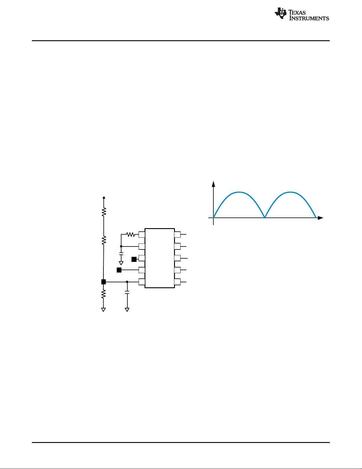
18 Circuit Analysis and Explanations
18.1 Injecting Line Voltage into Filter-2 (Achieving PFC > 0.95)
If a small portion (750mV to 1.00V) of line voltage is injected at FLTR2 of the LM3445, the circuit is
essentially turned into a constant power flyback as shown in Figure 34.
The LM3445 works as a constant off-time controller normally, but by injecting the 1.0V rectified AC voltage
into the FLTR2 pin, the on-time can be made to be constant. With a DCM Flyback, Δi needs to increase
as the input voltage line increases. Therefore a constant on-time (since inductor L is constant) can be
obtained.
By using the line voltage injection technique, the FLTR2 pin has the voltage wave shape shown in
Figure 35 on it with no TRIAC dimmer in-line. Voltage at V
current limit is tripped. C11 is small enough not to distort the AC signal but adds a little filtering.
Although the on-time is probably never truly constant, it can be observed in Figure 36 how (by adding the
rectified voltage) the on-time is adjusted.
peak should be kept below 1.25V. At 1.25V
FLTR2
www.ti.com
For this evaluation board, the following resistor values are used:
R2 = R7 = 309kΩ
R15 = 3.48kΩ
Therefore the voltages observed on the FLTR2 pin will be as follows for listed input voltages:
For VIN = 90V
For VIN = 120V
For VIN = 135V
Using this technique, a power factor greater than 0.95 can be achieved without additional passive active
power factor control (PFC) circuitry.
26
AN-2034 LM3445 -120VAC, 8W Isolated Flyback LED Driver SNVA429C–August 2010–Revised May 2013
Figure 34. Line Voltage Injection Circuit Figure 35. FLTR2 Waveform with No Dimmer
, V
RMS
RMS
RMS
FLTR2
, V
FLTR2
, V
FLTR2
= 0.71V
= 0.95V
= 1.07V
Copyright © 2010–2013, Texas Instruments Incorporated
Submit Documentation Feedback
Page 27

R
FLTR1
R
SNS
PWM
I-LIM
1.25V
I
SNS
ASNS
PGND
FLTR1
FLTR2
DIM
DIM DECODER
4.5V
Tri-State
50k
333k
C
FLTR2
C
FLTR1
1k
RAMP GEN.
5.5 kHz
3V
1V
750 mV
110 ns
LEADING EDGE BLANKING
1V
Nearly a constant on-
time as the line varies
The PWM reference increases
as the line voltage increases.
As line voltage increases, the voltage across the
inductor increases, and the peak current increases.
1V
D x LED Current
www.ti.com
Circuit Analysis and Explanations
Figure 36. Typical Operation of FLTR2 Pin
SNVA429C–August 2010–Revised May 2013 AN-2034 LM3445 -120VAC, 8W Isolated Flyback LED Driver
Submit Documentation Feedback
Copyright © 2010–2013, Texas Instruments Incorporated
27
Page 28

IMPORTANT NOTICE
Texas Instruments Incorporated and its subsidiaries (TI) reserve the right to make corrections, enhancements, improvements and other
changes to its semiconductor products and services per JESD46, latest issue, and to discontinue any product or service per JESD48, latest
issue. Buyers should obtain the latest relevant information before placing orders and should verify that such information is current and
complete. All semiconductor products (also referred to herein as “components”) are sold subject to TI’s terms and conditions of sale
supplied at the time of order acknowledgment.
TI warrants performance of its components to the specifications applicable at the time of sale, in accordance with the warranty in TI’s terms
and conditions of sale of semiconductor products. Testing and other quality control techniques are used to the extent TI deems necessary
to support this warranty. Except where mandated by applicable law, testing of all parameters of each component is not necessarily
performed.
TI assumes no liability for applications assistance or the design of Buyers’ products. Buyers are responsible for their products and
applications using TI components. To minimize the risks associated with Buyers’ products and applications, Buyers should provide
adequate design and operating safeguards.
TI does not warrant or represent that any license, either express or implied, is granted under any patent right, copyright, mask work right, or
other intellectual property right relating to any combination, machine, or process in which TI components or services are used. Information
published by TI regarding third-party products or services does not constitute a license to use such products or services or a warranty or
endorsement thereof. Use of such information may require a license from a third party under the patents or other intellectual property of the
third party, or a license from TI under the patents or other intellectual property of TI.
Reproduction of significant portions of TI information in TI data books or data sheets is permissible only if reproduction is without alteration
and is accompanied by all associated warranties, conditions, limitations, and notices. TI is not responsible or liable for such altered
documentation. Information of third parties may be subject to additional restrictions.
Resale of TI components or services with statements different from or beyond the parameters stated by TI for that component or service
voids all express and any implied warranties for the associated TI component or service and is an unfair and deceptive business practice.
TI is not responsible or liable for any such statements.
Buyer acknowledges and agrees that it is solely responsible for compliance with all legal, regulatory and safety-related requirements
concerning its products, and any use of TI components in its applications, notwithstanding any applications-related information or support
that may be provided by TI. Buyer represents and agrees that it has all the necessary expertise to create and implement safeguards which
anticipate dangerous consequences of failures, monitor failures and their consequences, lessen the likelihood of failures that might cause
harm and take appropriate remedial actions. Buyer will fully indemnify TI and its representatives against any damages arising out of the use
of any TI components in safety-critical applications.
In some cases, TI components may be promoted specifically to facilitate safety-related applications. With such components, TI’s goal is to
help enable customers to design and create their own end-product solutions that meet applicable functional safety standards and
requirements. Nonetheless, such components are subject to these terms.
No TI components are authorized for use in FDA Class III (or similar life-critical medical equipment) unless authorized officers of the parties
have executed a special agreement specifically governing such use.
Only those TI components which TI has specifically designated as military grade or “enhanced plastic” are designed and intended for use in
military/aerospace applications or environments. Buyer acknowledges and agrees that any military or aerospace use of TI components
which have not been so designated is solely at the Buyer's risk, and that Buyer is solely responsible for compliance with all legal and
regulatory requirements in connection with such use.
TI has specifically designated certain components as meeting ISO/TS16949 requirements, mainly for automotive use. In any case of use of
non-designated products, TI will not be responsible for any failure to meet ISO/TS16949.
Products Applications
Audio www.ti.com/audio Automotive and Transportation www.ti.com/automotive
Amplifiers amplifier.ti.com Communications and Telecom www.ti.com/communications
Data Converters dataconverter.ti.com Computers and Peripherals www.ti.com/computers
DLP® Products www.dlp.com Consumer Electronics www.ti.com/consumer-apps
DSP dsp.ti.com Energy and Lighting www.ti.com/energy
Clocks and Timers www.ti.com/clocks Industrial www.ti.com/industrial
Interface interface.ti.com Medical www.ti.com/medical
Logic logic.ti.com Security www.ti.com/security
Power Mgmt power.ti.com Space, Avionics and Defense www.ti.com/space-avionics-defense
Microcontrollers microcontroller.ti.com Video and Imaging www.ti.com/video
RFID www.ti-rfid.com
OMAP Applications Processors www.ti.com/omap TI E2E Community e2e.ti.com
Wireless Connectivity www.ti.com/wirelessconnectivity
Mailing Address: Texas Instruments, Post Office Box 655303, Dallas, Texas 75265
Copyright © 2013, Texas Instruments Incorporated
 Loading...