

Page 1
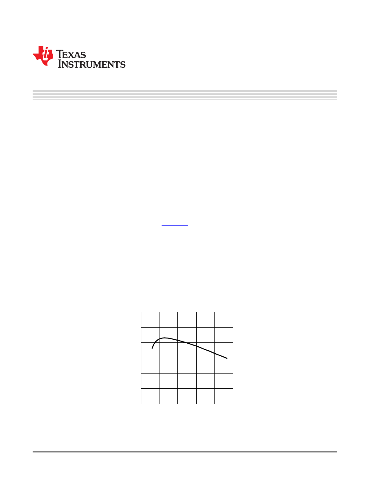
VIN (V)
EFFICIENCY (%)
100
95
90
85
80
75
70
0 16 32 48 64 80
1 Introduction
This wide range evaluation board showcases the LM3424 NFET controller used with a buck-boost current
regulator. It is designed to drive 4 to 10 LEDs at a maximum average LED current of 1A from a DC input
voltage of 10 to 70V.
The evaluation board showcases many of the LM3424 features including thermal foldback, analog
dimming, external switching frequency synchronization, and high frequency PWM dimming, among others.
There are many external connection points to facilitate the full evaluation of the LM3424 device including
inputs, outputs and test points. Refer to Table 1 for a summary of the connectors and test points.
The buck-boost circuit can be easily redesigned for different specifications by changing only a few
components (see the Alternate Designs section). Note that design modifications can change the system
efficiency for better or worse.
This application note is designed to be used in conjunction with the LM3424 datasheet as a reference for
the LM3424 buck-boost evaluation board. Refer to the LM3424 Constant Current N-Channel Controller
with Thermal Foldback for Driving LEDs (SNVS603) data sheet for a comprehensive explanation of the
device, design procedures, and application information.
User's Guide
SNVA397A–August 2009–Revised May 2013
AN-1967 LM3424 Buck-Boost Evaluation Board
2 Key Features
• Input: 10V to 70V
• Output: 4 to 10 LEDs at 1A
• Thermal Foldback / Analog Dimming
• PWM Dimming up to 10 kHz
• External Synchronization > 500 kHz
• Input Under-voltage and Output Over-voltage Protection
All trademarks are the property of their respective owners.
SNVA397A–August 2009–Revised May 2013 AN-1967 LM3424 Buck-Boost Evaluation Board
Submit Documentation Feedback
Figure 1. Efficiency with 9 Series LEDS AT 1A
1
Copyright © 2009–2013, Texas Instruments Incorporated
Page 2
External Connection Descriptions
3 External Connection Descriptions
Table 1. Connectors and Test Points
Qty Name Description Application Information
J1 V
IN
J2 GND Input Ground Connect to negative terminal of supply voltage (GND).
J3 EN Enable On/Off Jumper connected enables device.
J4 LED+ LED Positive Connect to anode (top) of LED string.
J5 LED- LED Negative Connect to cathode (bottom) of LED string.
J6 BNC Dimming Input Connect a 3V to 10V PWM input signal up to 10 kHz for PWM dimming the LED load.
J7 OUT Output with NTC Alternative connector for LED+ and LED-. Pins 4 and 11 are used for connecting an
TP1 SW Switch Node Test point for switch node (where Q1, D1, and L1 connect).
TP3 SGND Signal Ground Connection for GND when applying signals to TP5, TP8, and TP9.
TP4 LED+ LED Positive Test point for anode (top) of LED string.
TP5 nDIM Inverted Dim Signal Test point for dimming input (inverted from input signal).
TP6 V
IN
TP8 SYNC Synchronization Connect a 3V to 6V PWM clock signal > 500 kHz (pulse width of 100ns) to synchronize
TP9 NTC Temp Sense Input Connect a 0V to 1.24V DC voltage to analog dim the LED current.
TP10 PGND Power Ground Test point for GND when monitoring TP1, TP4, or TP6.
Input Voltage Connect to positive terminal of supply voltage.
external NTC thermistor. Refer to schematic for detailed connectivity.
Voltage
Voltage
Input Voltage Test point for input voltage.
Input the LM3424 switching frequency to the external clock.
www.ti.com
2
AN-1967 LM3424 Buck-Boost Evaluation Board SNVA397A–August 2009–Revised May 2013
Copyright © 2009–2013, Texas Instruments Incorporated
Submit Documentation Feedback
Page 3
SS
TGAIN
OVP
LM3424
nDIM
GND
TSENSE
TREF
DDRV
VS
DAP
GATE
EN
COMP
VIN
CSH
RT/SYNC
IS
HSN
SLOPE
VCC
HSP
Q7
D1
L1
R14
C9
R6
Q1
C7
R17
R11
R13
R5
R15
NTC
R19
R21
R22
1
2
3
4
5
6
7
8
9
10
20
19
18
17
16
15
14
13
12
11
R8
R7
C22
R9
R20
C12
C11
C15
Q3
PWM
R4
Q6
Q5
Q4
D2
V
IN
LED+
V
IN
DIM
DIM
R24
R23
Q2
C4,
C5,
C6,
C17,
C19
C2,
C3,
C16,
C18,
C23
C1
R3
J3
R12
J6
TP5
R2
C8
R1
R10
3
4
5
C10
C13
C14
R25
TP3 TP10
TP8
TP6
TP1
TP4
V
IN
J1
GND
J2
R26
C20
C21
8
9
10
12
13
14
7
6
5
3
2
1
J7
11 4
LED-
J4
J5
NTC
www.ti.com
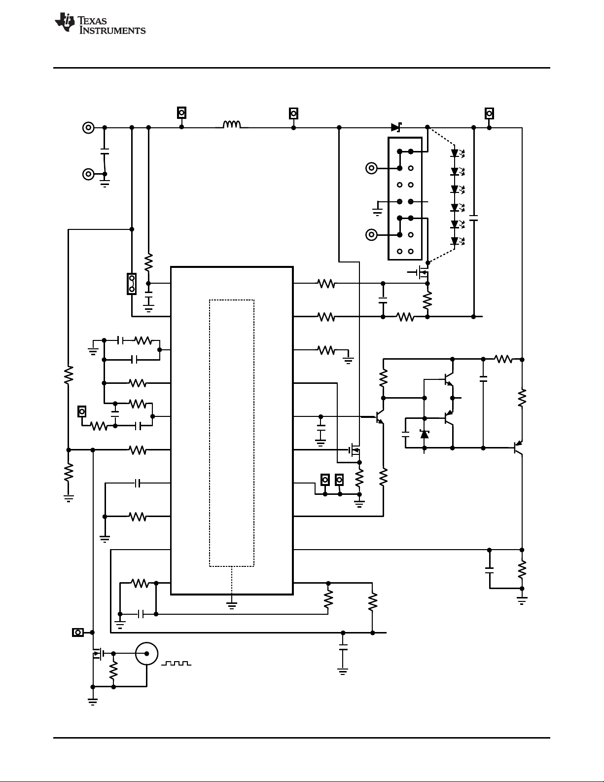
4 Schematic
Schematic
SNVA397A–August 2009–Revised May 2013 AN-1967 LM3424 Buck-Boost Evaluation Board
Submit Documentation Feedback
Copyright © 2009–2013, Texas Instruments Incorporated
3
Page 4

LM3424 Pin Descriptions
5 LM3424 Pin Descriptions
Pin Name Description Application Information
1 V
2 EN Enable the device or to < 0.8V for low
3 COMP Compensation
4 CSH Current Sense High
5 RT Resistor Timing synchronize external clock as
6 nDIM Not DIM input
7 SS Soft-start
8 TGAIN Temperature Foldback Gain
9 TSENSE Temperature Sense Input
10 TREF VSto set the temperature
11 V
12 OVP Over-Voltage Protection Turn-off threshold is 1.24V and
13 DDRV Dimming Gate Drive Output
14 GND Ground
15 GATE Gate Drive Output
www.ti.com
Bypass with 100 nF capacitor
IN
Input Voltage
to GND as close to the device
as possible in the circuit board
layout.
Connect to > 2.4V to enable
power shutdown.
Connect a capacitor to GND to
compensate control loop.
Connect a resistor to GND to
set the signal current. Can also
be used to analog dim as
explained in the Thermal
Foldback / Analog Dimming
section of the datasheet.
Connect a resistor to GND to
set the switching frequency.
Can also be used to
explained in the Switching
Frequency section of the
datasheet.
Connect a PWM signal for
dimming as detailed in the
PWM Dimming section of the
datasheet and/or a resistor
divider from VINto program
input under-voltage lockout
(UVLO). Turn-on threshold is
1.24V and hysteresis for turnoff is provided by 20 µA current
source.
Connect a capacitor to GND to
extend start-up time.
Connect a resistor to GND to
set the foldback slope.
Connect a resistor/ thermistor
divider from VSto sense the
temperature as explained in
the Thermal Foldback / Analog
Dimming section of the
datasheet.
Temperature Foldback
Reference
Connect a resistor divider from
foldback reference voltage.
2.45V reference for
S
Voltage Reference temperature foldback circuit
and other external circuitry.
Connect to a resistor divider
from VOto program output
over-voltage lockout (OVLO).
hysteresis for turn-on is
provided by 20 µA current
source.
Connect to gate of dimming
MosFET.
Connect to DAP to provide
proper system GND
Connect to gate of main
switching MosFET.
4
AN-1967 LM3424 Buck-Boost Evaluation Board SNVA397A–August 2009–Revised May 2013
Submit Documentation Feedback
Copyright © 2009–2013, Texas Instruments Incorporated
Page 5

www.ti.com
Pin Name Description Application Information
16 V
17 IS Main Switch Current Sense switch for R
18 SLOPE Slope Compensation
19 HSN resistor to the negative side of
20 HSP resistor to the positive side of
DAP (21) DAP Thermal pad on bottom of IC 9 vias to bottom layer ground
6 Bill of Materials
Qty Part ID Part Value Manufacturer Part Number
4 C1, C5, C20, C23 0.1 µF X7R 10% 100V TDK C2012X7R2A104K
4 C2, C3, C16, C18 4.7 µF X7R 10% 100V TDK C5750X7R2A475K
4 C4, C6, C17, C19 10 µF X7R 10% 50V TDK C5750X7R1H106K
2 C7, C22 0.47 µF X7R 10% 16V MURATA GRM21BR71C474KA01L
0 C8 DNP
1 C9 2.2 µF X7R 10% 16V MURATA GRM21BR71C225KA12L
1 C10 1 µF X7R 10% 16V MURATA GRM21BR71C105KA01L
1 C11 47 pF COG/NPO 5% 50V AVX 08055A470JAT2A
1 C12 0.22 µF X7R 10% 16V MURATA GRM219R71C224KA01D
3 C13, C14, C21 100 pF COG/NPO 5% 50V MURATA GRM2165C1H101JA01D
1 C15 1 µF X7R 10% 16V MURATA GRM21BR71C105MA01L
1 D1 Schottky 100V 12A VISHAY 12CWQ10FNPBF
1 D2 Zener 10V ON-SEMI BZX84C10LT1G
4 J1, J2, J4, J5 Banana Jack KEYSTONE 575-8
1 J3 1x2 Header Male SAMTEC TSW-102-07-T-S
1 J6 BNC connector AMPHENOL 112536
1 J7 2x7 Header Male Shrouded SAMTEC TSSH-107-01-SDRA
1 L1 33 µH 20% 6.3A COILCRAFT MSS1278-333MLB
2 Q1, Q2 NMOS 100V 32A FAIRCHILD FDD3682
1 Q3 NMOS 60V 260mA ON-SEMI 2N7002ET1G
1 Q4 PNP 40V 200mA FAIRCHILD MMBT5087
1 Q5 PNP 150V 600 mA FAIRCHILD MMBT5401
1 Q6 NPN 300V 600mA FAIRCHILD MMBTA42
1 Q7 NPN 40V 200mA FAIRCHILD MMBT6428
2 R1, R11 12.4 kΩ 1% VISHAY CRCW080512K4FKEA
0 R2 DNP
3 R3, R20, R26 10Ω 1% VISHAY CRCW080510R0FKEA
1 R4 17.4 kΩ 1% VISHAY CRCW080517K4FKEA
1 R5 1.43 kΩ 1% VISHAY CRCW08051K43FKEA
CC
RA
Internal Regulator Output
High-Side LED Current Sense
Negative
High-Side LED Current Sense
Positive
Bill of Materials
Bypass with a 2.2 µF–3.3 µF,
ceramic capacitor to GND.
Connect to the drain of the
main N-channel MosFET
a sense resistor installed in the
source of the same device.
Connect a resistor to GND to
set slope of additional ramp.
Connect through a series
the LED current sense resistor.
Connect through a series
the LED current sense resistor.
Connect to GND and place 6 pour.
sensing or to
DS-ON
SNVA397A–August 2009–Revised May 2013 AN-1967 LM3424 Buck-Boost Evaluation Board
Submit Documentation Feedback
Copyright © 2009–2013, Texas Instruments Incorporated
5
Page 6

Bill of Materials
www.ti.com
1 R6 0.04Ω 1% 1W VISHAY WSL2512R0400FEA
2 R7, R8 1.0 kΩ 1% VISHAY CRCW08051K00FKEA
1 R9 0.1Ω 1% 1W VISHAY WSL2512R1000FEA
1 R10 14.3 kΩ 1% VISHAY CRCW080514K3FKEA
4 R12, R13, R14, R15 10.0 kΩ 1% VISHAY CRCW080510K0FKEA
1 R17 499 kΩ 1% VISHAY CRCW0805499KFKEA
3 R19, R21, R22 49.9 kΩ 1% VISHAY CRCW080549K9FKEA
1 R23 499Ω 1% VISHAY CRCW0805499RFKEA
1 R24 4.99 kΩ 1% VISHAY CRCW08054K99FKEA
1 R25 150Ω 1% VISHAY CRCW0805150RFKEA
8 TP1, TP3, TP4, Turret Keystone 1502-2
TP5, TP6, TP8,
TP9, TP10
1 U1 Buck-boost controller TI LM3424
6
AN-1967 LM3424 Buck-Boost Evaluation Board SNVA397A–August 2009–Revised May 2013
Copyright © 2009–2013, Texas Instruments Incorporated
Submit Documentation Feedback
Page 7

www.ti.com
7 PCB Layout
PCB Layout
Figure 2. Top Layer
Figure 3. Bottom Layer
SNVA397A–August 2009–Revised May 2013 AN-1967 LM3424 Buck-Boost Evaluation Board
Submit Documentation Feedback
Copyright © 2009–2013, Texas Instruments Incorporated
7
Page 8

R10 = =
= 14.4 k:
1 + 1.95e-8 x f
SW
1.40e
-10
x f
SW
1 + 1.95e-8 x 500 kHz
1.40e
-10
x 500 kHz
D
MAX
==
677.0
=
V21
V10V21 +
V
O
VV
IN-MINO
+
21V
=
21V + 70V
= 0.231
D
MIN
=
VO + V
IN-MAX
V
O
533.0467.01D1'D
=
-
=
-
=
D
==
467.0
=
V21
V24V21 +
V
O
VV
INO
+
:
=
:x
=
x
=
95.1m3256rNr
LEDD
V21V5.36VNV
LEDO
=
x
=
x
=
Design Procedure
8 Design Procedure
8.1 Specifications
N = 6
V
= 3.5V
LED
r
= 325 mΩ
LED
VIN= 24V
V
= 10V
IN-MIN
V
fSW= 500 kHz
V
I
Δi
Δi
Δv
I
V
V
V
V
TBK= 45°C
T
t
IN-MAX
SNS
= 1A
LED
L-PP
LED-PP
IN-PP
= 6A
LIM
TURN-ON
HYS
TURN-OFF
HYSO
= 125°C
END
= 40 ms
TSU
= 70V
= 100 mV
= 700 mA
= 12 mA
= 100 mV
= 10V
= 3V
= 50V
= 10V
www.ti.com
8.2 Operating Point
8.3 Switching Frequency
8
Solve for VOand rD:
(1)
(2)
Solve for D, D', D
MAX
, and D
MIN
:
(3)
(4)
(5)
(6)
Solve for RT:
(7)
AN-1967 LM3424 Buck-Boost Evaluation Board SNVA397A–August 2009–Revised May 2013
Copyright © 2009–2013, Texas Instruments Incorporated
Submit Documentation Feedback
Page 9

PP-==L
DVINx
f1LSWx
kHz045H33 xP
467.0V42 x
mA674
=
'i
==
DVINx
fSWx
467.0V42 x
PH
32
=
1L
PP-'iL
kHz045700 mA x
R15 = 10 k:
R19 = R21 = R22 = 49.9 k:
R
GAIN
=
R19
x 2.45V
100 PA
R19 + R21
-
¸
¸
¹
·
¸
¸
¹
·
R
NTC-END
R
NTC-END
+ R22
I
CSH
= 9.49 k:
R
GAIN
=
1
x 2.45V
2
-
¸
¸
¹
·
¸
¸
¹
·
6.34 k: + 49.9 k:
6.34 k:
R8 = R7 = 1 k:
R1 = 12.4 k:
R9 = 0.1:
LED
=
= = 1.0A
1.24V x R8
R9 x R1
1.24V x 1.0 k:
0.1: x 1.24 k:
= 1.0 k:
I
LED
x R1 x R9
1.24V
1A x 1.24 k: x 0.1:
= 0.1:
V
SNS
100 mV
1A
I
LED
R10 = 14.3 k:
fSW =
= 504 kHz
1.40e
-10
x 14.3 k: - 1.95e
-8
1
fSW =
1.40e
-10
x R10 - 1.95e
-8
1
www.ti.com
The closest standard resistor is 14.3 kΩ therefore fSWis:
The chosen component from step 2 is:
8.4 Average LED Current
Design Procedure
(8)
(9)
Solve for R
Assume R
:
SNS
= 12.4 kΩ and solve for R
CSH
The closest standard resistor for R
The chosen components from step 3 are:
8.5 Thermal Foldback
Using a standard 100k NTC thermistor (connected to pins 4 and 11 of J7), find the resistances
corresponding to TBKand T
datasheet. Assuming R
Solve for R
GAIN
:
END(RNTC-BK
= R
REF1
:
HSP
is actually 0.1Ω and for R
SNS
= 243 kΩ and R
= 49.9 kΩ, then R
REF2
NTC-END
BIAS
is actually 1 kΩ therefore I
HSP
= 71.5 kΩ) from the manufacturer's
= R
NTC-BK
= 243 kΩ.
LED
(10)
(11)
is:
(12)
(13)
The chosen components from step 4 are:
8.6 Inductor Ripple Current
Solve for L1:
The closest standard inductor is 33 µH therefore Δi
SNVA397A–August 2009–Revised May 2013 AN-1967 LM3424 Buck-Boost Evaluation Board
Submit Documentation Feedback
is:
L-PP
Copyright © 2009–2013, Texas Instruments Incorporated
(14)
(15)
(16)
(17)
9
Page 10

= 9.9 k:
R15 =
VO x R10 x R9
R15 =
1.5e13 x L1
35V x 14.3 k: x 0.1:
1.5e13 x 33 PH
R6 = 0.04:
=
0.04:
= 6.13A
I
LIM
=
R6
245 mV 245 mV
=
6A
= 0.041:
R6 =
I
LIM
245 mV 245 mV
C4 = C6 = C17 = C19 = 10 PF
x
A1
=
I
LED
I
RMSCO-
=
1- 0.677
677.0
1.45A
x
1- D
MAX
D
MAX
=
DI
LED
x
=
'i
PP-LED
SW
fxrDx
C
O
2
= =
kHz04595.1 xx:
1 mA
467.0A1 x
F40 P
'i
PP-LED
f
'i
r
SWPP-LEDD
xx
DI
LED
x
CO=
2
= F39.6P=
kHz045mA195.1 xx:
467.0A1 x
C
O
H331L P
=
A89.1
12
1
1
I
RMSL
=
+
x
=
-
I
I
LED
RMSL
x
=
-
12
1
1
2
x
+
¸
¸
¹
·
¨
¨
©
§
Di
PPL
c
x
'
-
I
LED
D
c
533.0mA674
2
x
¸
¸
¹
·
¨
¨
©
§
A1
x
533.0
A1
Design Procedure
Determine minimum allowable RMS current rating:
The chosen component from step 5 is:
8.7 Output Capacitance
Solve for CO:
The closest capacitance totals 40 µF therefore Δi
LED-PP
www.ti.com
(18)
(19)
(20)
is:
Determine minimum allowable RMS current rating:
The chosen components from step 6 are:
8.8 Peak Current Limit
Solve for R
The closest standard resistor is 0.04 Ω therefore I
The chosen component from step 7 is:
LIM
:
8.9 Slope Compensation
Solve for R
SLP
:
LIM
(21)
(22)
(23)
(24)
is:
(25)
(26)
The chosen component from step 8 is:
10
AN-1967 LM3424 Buck-Boost Evaluation Board SNVA397A–August 2009–Revised May 2013
(27)
Copyright © 2009–2013, Texas Instruments Incorporated
Submit Documentation Feedback
Page 11

C2 = C3 = C16 = C18 = 4.7 PF
x
A1
=
I
LED
I
RMSIN-
=
1- 0.677
677.0
1.45A
x
1- D
MAX
D
MAX
=
C
IN
==
kHz504mV100 x
467.0A1 x
F27.9 P=
f
'v
SWPPIN-
x
DI
LED
x
C12 = 0.22 PF
C10 = 1 PF
R20 = 10:
C12 = =
= 0.28 PF
1
10:xZP3
1
rad
sec
10:x 360k
1010(max
1P
xZ
=
x
=
,
1Z1P
ZZ
sec
rad
k36
sec
rad
k36010=x
=
3P
Z
3P
Z
)
C10 = =
= 0.30 PF
1
Z
P2
x 5e
6
:
1
0.675 x 5e
6
:
rad
sec
= =
sec
rad
675.0=
sec
rad
k19
56305 x56305x
1Z
Z
2P
=Z
),min(
1Z1P
ZZ
T50Ux
TU0 =
= = 5630
D' x 620V
(1 + D) x I
LED
x R6
0.533 x 620V
1.467 x 1A x 0.04:
sec
rad
k36===
533.095.12x:
H33467.0 Px
Dr
2
D
c
x
L1Dx
1Z
Z
sec
rad
k19===
1.467
F40
1.95:
Px
COrDx
D1+
1P
Z
R
SLP
= 10 k:
www.ti.com
8.10 Loop Compensation
ω
is approximated:
P1
ω
is approximated:
Z1
TU0is approximated:
To ensure stability, calculate ωP2:
Solve for C
CMP
:
Design Procedure
(28)
(29)
(30)
(31)
(32)
To attenuate switching noise, calculate ωP3:
Assume RFS= 10Ω and solve for CFS:
The chosen components from step 9 are:
8.11 Input Capacitance
Solve for the minimum CIN:
To minimize power supply interaction a 200% larger capacitance of approximately 20 µF is used, therefore
the actual Δv
capacitors are chosen.
Determine minimum allowable RMS current rating:
is much lower. Since high voltage ceramic capacitor selection is limited, four 4.7 µF X7R
IN-PP
(33)
(34)
(35)
(36)
(37)
The chosen components from step 10 are:
SNVA397A–August 2009–Revised May 2013 AN-1967 LM3424 Buck-Boost Evaluation Board
Submit Documentation Feedback
(38)
(39)
11
Copyright © 2009–2013, Texas Instruments Incorporated
Page 12

V
TURN-ON
=
R5
1.24V x (1.43 k: + 10 k:)
1.43 k:
1.24V x (R5 + R13)
= 9.91V
V
TURN-ON
=
1.24V x R13
V
TURN-ON
- 1.24V
= 1.42 k:
R5 = =
1.24V x 10 k:
10V - 1.24V
HYS
=
R5
20 PA x 17.4 k: x (1.43 k: + 10 k:)
1.43 k:
HYS
=
+ 20 PA x R13
20 PA x R4 x (R5 + R13)
+ 20 PA x 10 k: = 2.98V
R4 =
R5 x (V
HYS
- 20 PA x R13)
20 PA x (R5 + R13)
= 17.5 k:
R4 =
1.43 k: x (3V - 20 PA x 10 k:)
20 PA x (1.43 k: + 10 k:)
D1 o 12A, 100V, DPAK
mW600mV600A1VIP
FDDD
=
x
=
x
=
A1II
LEDMAXD==-
V91V21V70VVV
OMAXINMAXRD
=
+
=
+
=
--
Q1 o 32A, 100V, DPAK
mW82m50A28.1RIP
2
DSON
2
RMSTT
=
:x
=
x
=
-
x
I
RMST=-
I
LED
D
c
=
x
A28.1
=
0.467
A1
533.0
D
=
A2.1A1=x
677.01-
677.0
I
MAXT-
V91V21V70VVV
OMAXINMAXT
=+=+=
--
Design Procedure
8.12 NFET
Determine minimum Q1 voltage rating and current rating:
A 100V NFET is chosen with a current rating of 32A due to the low R
PT:
The chosen component from step 11 is:
8.13 Diode
Determine minimum D1 voltage rating and current rating:
= 50 mΩ. Determine I
DS-ON
www.ti.com
and
T-RMS
(40)
(41)
(42)
(43)
(44)
(45)
A 100V diode is chosen with a current rating of 12A and VD= 600 mV. Determine PD:
The chosen component from step 12 is:
8.14 Input UVLO
Solve for R
The closest standard resistor is 150 kΩ therefore V
Solve for R
UV2
UV1
(46)
(47)
(48)
:
(49)
is:
HYS
(50)
:
The closest standard resistor is 21 kΩ making V
12
AN-1967 LM3424 Buck-Boost Evaluation Board SNVA397A–August 2009–Revised May 2013
(51)
:
TURN-ON
(52)
Copyright © 2009–2013, Texas Instruments Incorporated
Submit Documentation Feedback
Page 13

CSS = 0.47 PF
CSS =
= = 540 nF
(40 ms - 29.2 ms)
(t
TSU
- t
SU-SS-BASE
)
20 k: 20 k:
V
O
I
LED
t
SU-SS-BASE
= 168: x C9 + 28 k:x C10 + x C
O
t
SU-SS-BASE
= 29.2 ms
21V
1A
t
SU-SS-BASE
= 168: x 2.2 PF + 28 k:x 1.0 PF + x 40 PF
V
O
I
LED
tSU = 168: x C9 + 36 k:x C10 + x C
O
tSU = 37.2 ms
21V
1A
tSU = 168: x 2.2 PF + 36 k:x 1.0 PF + x 40 PF
R11 = 12.4 k:
R17 = 499 k:
= 51.1V
12.4 k:
1.24V x (12.4 k: + 499 k:)
V
TURN-OFF
=
R11
1.24V x (R11 + R17)
V
TURN-OFF
=
R11 = =
= 12.5 k:
V
TURN-OFF
- 1.24V
1.24V x R17
1.24V x 499 k:
50V - 620 mV
V
HYSO
= R17 x 20 PA = 499 k: x 20 PA = 9.98V
R17 =
=
= 500 k:
V
HYSO
10V
20 PA20 PA
R4 = 17.4 k:
R13 = 10 k:
R5 = 1.43 k:
www.ti.com
The chosen components from step 13 are:
8.15 Output OVLO
Design Procedure
(53)
Solve for R
The closest standard resistor is 499 kΩ therefore V
Solve for R
The closest standard resistor is 15.8 kΩ making V
The chosen components from step 14 are:
8.16 Soft-Start
Solve for tSU:
OV2
OV1
:
(54)
is:
HYSO
(55)
:
(56)
TURN-OFF
:
(57)
(58)
If tSUis less than t
, solve for t
TSU
Solve for CSS:
The chosen component from step 15 is:
SNVA397A–August 2009–Revised May 2013 AN-1967 LM3424 Buck-Boost Evaluation Board
Submit Documentation Feedback
SU-SS-BASE
Copyright © 2009–2013, Texas Instruments Incorporated
:
(59)
(60)
(61)
(62)
13
Page 14

I
LED
(A)
V
SW
(V)
60
40
20
0
1.0
0.5
0.0
I
LED
2 Ps/DIV
V
SW
I
LED
(A)
V
DIM
(V)
10
5
0
1.0
0.0
-1.0
I
LED
V
DIM
4 ms/DIV
Typical Waveforms
9 Typical Waveforms
TA= +25°C, VIN= 24V and VO= 21V.
Figure 4. Standard Operation Figure 5. 200Hz 50% PWM Dimming
TP1 Switch Node Voltage (VSW) TP5 Dim Voltage (V
LED Current (I
) LED Current (I
LED
LED
www.ti.com
)
DIM
)
10 Alternate Designs
Alternate designs with the LM3429 evaluation board are possible with very few changes to the existing
hardware. The evaluation board FETs and diodes are already rated higher than necessary for design
flexibility. The input UVLO, output OVP, input and output capacitance can remain the same for the designs
shown below. These alternate designs can be evaluated by changing only R9, R10, and L1.
Table 2 gives the main specifications for four different designs and the corresponding values for R9, R10,
and L1. PWM dimming can be evaluated with any of these designs.
Specification / Design 1 Design 2 Design 3 Design 4
Component
V
IN
V
O
f
SW
I
LED
R9 0.05Ω 0.2Ω 0.04Ω 0.08Ω
R10 12.1 kΩ 10.2 kΩ 14.3 kΩ 10.2 kΩ
L1 22µH 68µH 15µH 33µH
Table 2. Alternate Design Specifications
10V - 45V 15V - 50V 20V - 55V 25V - 60V
14V 21V 28V 35V
600kHz 700kHz 500kHz 700kHz
2A 500mA 2.5A 1.25A
14
AN-1967 LM3424 Buck-Boost Evaluation Board SNVA397A–August 2009–Revised May 2013
Copyright © 2009–2013, Texas Instruments Incorporated
Submit Documentation Feedback
Page 15

IMPORTANT NOTICE
Texas Instruments Incorporated and its subsidiaries (TI) reserve the right to make corrections, enhancements, improvements and other
changes to its semiconductor products and services per JESD46, latest issue, and to discontinue any product or service per JESD48, latest
issue. Buyers should obtain the latest relevant information before placing orders and should verify that such information is current and
complete. All semiconductor products (also referred to herein as “components”) are sold subject to TI’s terms and conditions of sale
supplied at the time of order acknowledgment.
TI warrants performance of its components to the specifications applicable at the time of sale, in accordance with the warranty in TI’s terms
and conditions of sale of semiconductor products. Testing and other quality control techniques are used to the extent TI deems necessary
to support this warranty. Except where mandated by applicable law, testing of all parameters of each component is not necessarily
performed.
TI assumes no liability for applications assistance or the design of Buyers’ products. Buyers are responsible for their products and
applications using TI components. To minimize the risks associated with Buyers’ products and applications, Buyers should provide
adequate design and operating safeguards.
TI does not warrant or represent that any license, either express or implied, is granted under any patent right, copyright, mask work right, or
other intellectual property right relating to any combination, machine, or process in which TI components or services are used. Information
published by TI regarding third-party products or services does not constitute a license to use such products or services or a warranty or
endorsement thereof. Use of such information may require a license from a third party under the patents or other intellectual property of the
third party, or a license from TI under the patents or other intellectual property of TI.
Reproduction of significant portions of TI information in TI data books or data sheets is permissible only if reproduction is without alteration
and is accompanied by all associated warranties, conditions, limitations, and notices. TI is not responsible or liable for such altered
documentation. Information of third parties may be subject to additional restrictions.
Resale of TI components or services with statements different from or beyond the parameters stated by TI for that component or service
voids all express and any implied warranties for the associated TI component or service and is an unfair and deceptive business practice.
TI is not responsible or liable for any such statements.
Buyer acknowledges and agrees that it is solely responsible for compliance with all legal, regulatory and safety-related requirements
concerning its products, and any use of TI components in its applications, notwithstanding any applications-related information or support
that may be provided by TI. Buyer represents and agrees that it has all the necessary expertise to create and implement safeguards which
anticipate dangerous consequences of failures, monitor failures and their consequences, lessen the likelihood of failures that might cause
harm and take appropriate remedial actions. Buyer will fully indemnify TI and its representatives against any damages arising out of the use
of any TI components in safety-critical applications.
In some cases, TI components may be promoted specifically to facilitate safety-related applications. With such components, TI’s goal is to
help enable customers to design and create their own end-product solutions that meet applicable functional safety standards and
requirements. Nonetheless, such components are subject to these terms.
No TI components are authorized for use in FDA Class III (or similar life-critical medical equipment) unless authorized officers of the parties
have executed a special agreement specifically governing such use.
Only those TI components which TI has specifically designated as military grade or “enhanced plastic” are designed and intended for use in
military/aerospace applications or environments. Buyer acknowledges and agrees that any military or aerospace use of TI components
which have not been so designated is solely at the Buyer's risk, and that Buyer is solely responsible for compliance with all legal and
regulatory requirements in connection with such use.
TI has specifically designated certain components as meeting ISO/TS16949 requirements, mainly for automotive use. In any case of use of
non-designated products, TI will not be responsible for any failure to meet ISO/TS16949.
Products Applications
Audio www.ti.com/audio Automotive and Transportation www.ti.com/automotive
Amplifiers amplifier.ti.com Communications and Telecom www.ti.com/communications
Data Converters dataconverter.ti.com Computers and Peripherals www.ti.com/computers
DLP® Products www.dlp.com Consumer Electronics www.ti.com/consumer-apps
DSP dsp.ti.com Energy and Lighting www.ti.com/energy
Clocks and Timers www.ti.com/clocks Industrial www.ti.com/industrial
Interface interface.ti.com Medical www.ti.com/medical
Logic logic.ti.com Security www.ti.com/security
Power Mgmt power.ti.com Space, Avionics and Defense www.ti.com/space-avionics-defense
Microcontrollers microcontroller.ti.com Video and Imaging www.ti.com/video
RFID www.ti-rfid.com
OMAP Applications Processors www.ti.com/omap TI E2E Community e2e.ti.com
Wireless Connectivity www.ti.com/wirelessconnectivity
Mailing Address: Texas Instruments, Post Office Box 655303, Dallas, Texas 75265
Copyright © 2013, Texas Instruments Incorporated
 Loading...