

Page 1
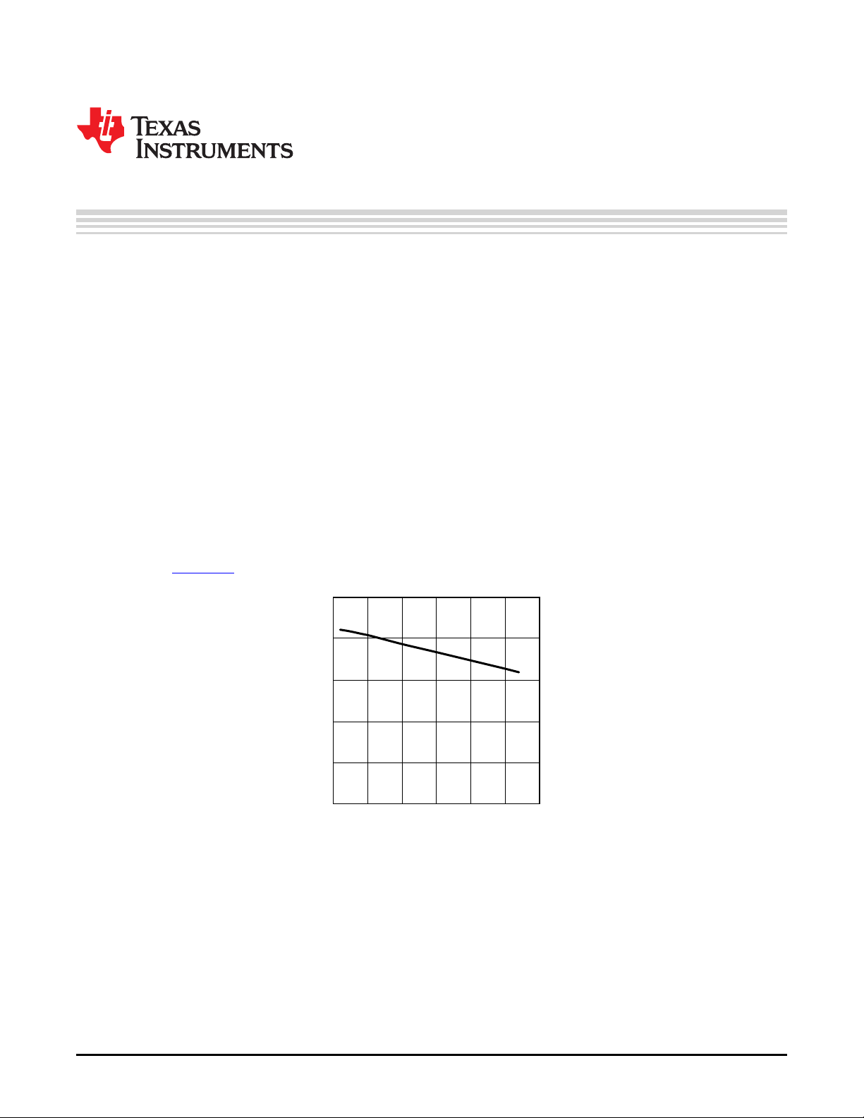
INPUT VOLTAGE (V)
EFFICIENCY (%)
100
95
90
85
80
75
15 20 25 30 35 40 45
1 Introduction
This demonstration board showcases the LM3409 PFET controller for a buck current regulator. It is
designed to drive 4 LEDs (VO= 15V) at a maximum average LED current (I
voltage (VIN= 24V). The switching frequency (fSW= 525 kHz) is targeted for the nominal operating point,
however fSWvaries across the entire operating range. The circuit can accept an input voltage of 6V-42V.
However, if the input voltage drops below the regulated LED string voltage, the converter goes into
dropout and VO= VINideally.
The PCB is made using 2 layers of 2 oz. copper with FR4 dielectric. The board showcases several
features of the LM3409 including both analog dimming using a potentiometer (R5) tied to the IADJ pin and
internal PWM dimming using the EN pin. There is a header (J1) with a removable jumper, which is used to
select PWM dimming or low power shutdown.
The board has a right angle connector (J2) which can mate with an external LED load board allowing for
the LEDs to be mounted close to the driver. This reduces potential ringing when there is no output
capacitor. Alternatively, the LED+ and LED- turrets can be used to connect the LED load.
This board can be easily modified to demonstrate other operating points as shown in Section 8. The
LM3409 / LM3409HV / LM3409Q / LM3409QHV / LM3409N PFET Buck Controller for High Power LED
Drivers (SNVS602) data sheet's Design Procedure can be used to design for any set of specifications.
User's Guide
SNVA391D–May 2009–Revised May 2013
AN-1954 LM3409 Demonstration Board
= 1A) from a DC input
LED
All trademarks are the property of their respective owners.
SNVA391D–May 2009–Revised May 2013 AN-1954 LM3409 Demonstration Board
Submit Documentation Feedback
Figure 1. Efficiency with 4 Series LEDS AT 1A
1
Copyright © 2009–2013, Texas Instruments Incorporated
Page 2
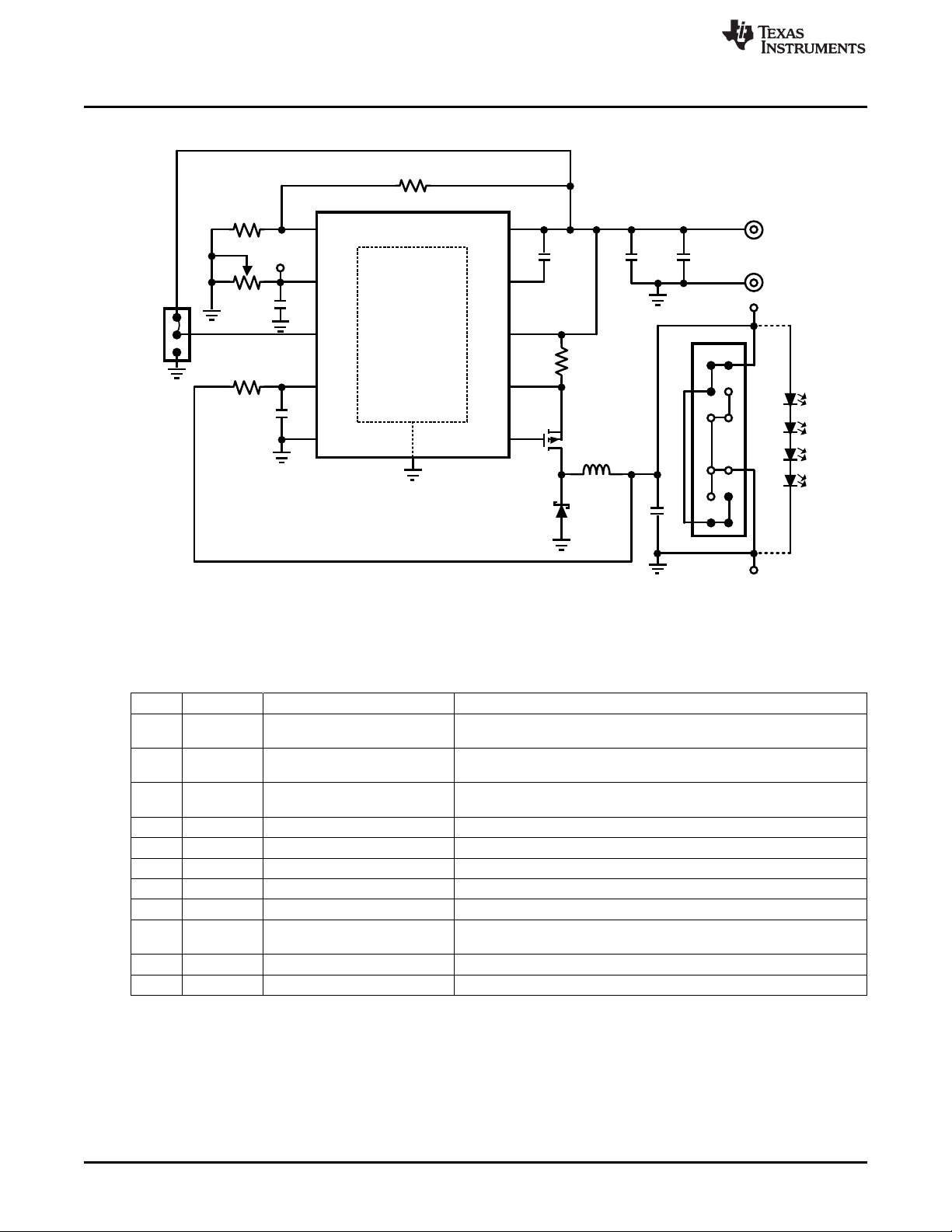
IADJ
EN
CSN
LM3409
UVLO
C1
V
IN
VCC
COFF
GND
CSP
C4
R1
PGATE
C3
R3
R2
DAP
VIN
R4
1
2
3
4
5 6
7
8
9
10
R5
C
5
GND
U1
C2
LED+
LED-
1
2
3
5
6
7
14
13
12
10
9
8
J2
D1
L1
Q1
J1
VADJ
C6
Schematic
2 Schematic
www.ti.com
Figure 2. Board Schematic
3 Pin Descriptions
Pin(s) Name Description Application Information
1 UVLO Input under-voltage lockout Connect to a resistor divider from VINand GND. Turn-on threshold is
2 IADJ Analog LED current adjust Apply a voltage between 0 - 1.24V, connect a resistor to GND, or leave
3 EN Logic level enable Apply a voltage >1.74V to enable device, a PWM signal to dim, or a
4 COFF Off-time programming Connect resistor to VO, and capacitor to GND to set the off-time.
5 GND Ground Connect to the system ground.
6 PGATE Gate drive Connect to the gate of the external PFET.
7 CSN Negative current sense Connect to the negative side of the sense resistor.
8 CSP Positive current sense Connect to the positive side of the sense resistor (VIN).
9 VCC VIN- referenced linear regulator Connect at least a 1µF ceramic capacitor to VIN. The regulator provides
2
10 VIN Input voltage Connect to the input voltage.
DAP DAP Thermal pad on bottom of IC Connect to pin 5 (GND). Place 4-6 vias from DAP to bottom GND plane.
AN-1954 LM3409 Demonstration Board SNVA391D–May 2009–Revised May 2013
output power for the PFET drive.
Copyright © 2009–2013, Texas Instruments Incorporated
1.24V and hysteresis for turn-off is provided by a 22µA current source.
open to set the current sense threshold voltage.
voltage <0.5V for low power shutdown.
Submit Documentation Feedback
Page 3
www.ti.com
4 Bill of Materials
Qty Part ID Part Value Manufacturer Part Number
1 U1 Buck controller Texas Instruments LM3409
1 C1 4.7µF X7R 20% 50V MURATA GRM55ER71H475MA01L
1 C2, C5 No Load
1 C3 470pF X7R 10% 50V TDK C1608X7R1H471K
1 C4 1.0µF X7R 10% 16V TDK C1608X7R1C105K
1 C6 0.1µF 50V 10% X7R MURATA C1608X7R1C104K
1 Q1 PMOS 70V 5.7A ZETEX ZXMP7A17KTC
1 D1 Schottky 60V 5A VISHAY CDBC560-G
1 L1 22 µH 20% 3.5A TDK SLF12565T-220M3R5
1 R1 15.4kΩ 1% VISHAY CRCW060315K4FKEA
1 R2 6.98kΩ 1% VISHAY CRCW06036K98FKEA
1 R3 49.9kΩ 1% VISHAY CRCW060349K9FKEA
1 R4 0.2Ω 1% 1W VISHAY WSL2512R2000FEA
1 R5 250kΩ potentiometer BOURNS 3352P-1-254
1 J1 MOLEX 22-28-4033
1 J2 SAMTEC TSSH-107-01-S-D-RA
2 VIN, GND KEYSTONE 575-8
3 VADJ, LED+, LED- KEYSTONE 1502-2
Bill of Materials
Table 1. Bill of Materials
SNVA391D–May 2009–Revised May 2013 AN-1954 LM3409 Demonstration Board
Submit Documentation Feedback
Copyright © 2009–2013, Texas Instruments Incorporated
3
Page 4
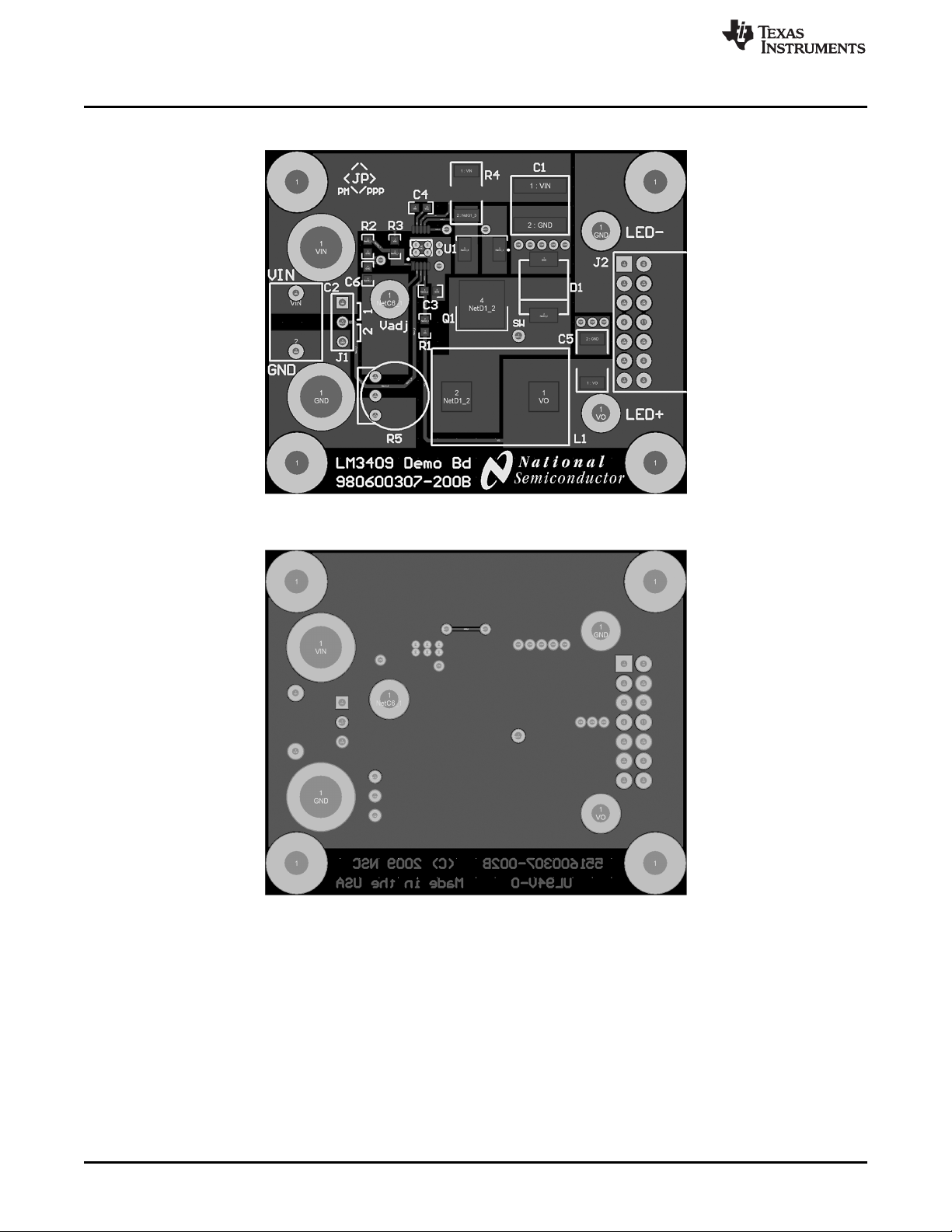
PCB Layout
5 PCB Layout
www.ti.com
Figure 3. Top Layer
Figure 4. Bottom Layer
4
AN-1954 LM3409 Demonstration Board SNVA391D–May 2009–Revised May 2013
Copyright © 2009–2013, Texas Instruments Incorporated
Submit Documentation Feedback
Page 5

H22L1 P
=
= =
H22 P
444
=
651nsV15 x
L1
tV
OFFO
x
i
PPL'-
mA
=
H7.21 P
=
L1
=
i
PPL'-
tV
OFFO
x
ns651V15 x
mA450
=
pF470C3
:
=
k4.15R1
t
OFF
fSW= =
ns651
=
kHz525
1
-
¸
¹
·
¨
©
§
V2495.0 x
V15
¸
¸
¹
·
¨
¨
©
§
V
O
VINxK
1
-
1lnk4.15pF490t
OFF
-x:x
-
=
¨
¨
©
§
ns651
=
¸
¸
¹
·
V24.1
V15
(C3+20pF)t
OFF
-
=
x R1 x11ln -
¸
¸
¹
·
¨
¨
©
§
V
O
V24.
=
R1
--
1
¸
¸
¹
·
¨
¨
©
§
V
O
xK V
IN
=
R1
:=k4.15
x lnpF490 xkHz525
¨
©
§
-
1
V15
¸
¹
·
V24.1
--
1
¨
©
§
¸
¹
·
V15
x V2495.0
-
xx 1lnf(C3 + 20 pF)
SW
¸
¸
¹
·
¨
¨
©
§
V
O
V24.1
www.ti.com
6 Design Procedure
6.1 Specifications
Design Procedure
VIN= 24V; V
IN-MAX
= 42V
VO= 15V
fSW= 525kHz
I
= 1A
LED
Δi
Δv
V
LED-PP
IN-PP
TURN-ON
= Δi
L-PP
= 720mV
= 10V; V
= 450mA
= 1.1V
HYS
η = 0.95
6.2 Nominal Switching Frequency
Assume C3 = 470pF and η = 0.95. Solve for R1:
The closest 1% tolerance resistor is 15.4 kΩ therefore the actual t
and target fSWare:
OFF
(1)
The chosen components from step 1 are:
6.3 Inductor Ripple Current
Solve for L1:
The closest standard inductor value is 22 µH therefore the actual Δi
The chosen component from step 2 is:
SNVA391D–May 2009–Revised May 2013 AN-1954 LM3409 Demonstration Board
Submit Documentation Feedback
Copyright © 2009–2013, Texas Instruments Incorporated
L-PP
is:
(2)
(3)
(4)
(5)
(6)
(7)
5
Page 6

=
mA670
=
A02.1V15 x
95.0V24 x
IDI
LEDT
=
x
=
VINKx
IV
LEDO
x
V42VV
MAXINMAXT
==
--
F7.4C1 P
=
I
RMSIN-
kHz525A02.1 xx
=
mA483
=
ns651s25.1 xP
tt
OFFON
xfII
SWLEDRMSIN
xx
=
-
2C
MININ
=
x
=
-
F54.3 PC
IN
C
MININ=-
= =
F77.1 P
mV720
A02.1 x s25.1 P
v
PPIN'-
tI
ONLED
x
1
t
ON
=
1
t
OFF
=
- - ns651
=
s25.1 P
kHz525
f
SW
=
R4
:2.0
I
LED
=
2
444
-
A02.1
=
2.05 :x
V24.1
I
LED
=
R45x
-
2
i
PPL'-
V
ADJ
mA
=
R4
V
ADJ
x-I5
MAXL
= =
:203.0
V24.1
x5 A22.1
II
LEDMAXL
+
=
-
2
A1
+
=
A22.1
=
2
i
PPL'-
444
mA
Design Procedure
6.4 Average LED Current
www.ti.com
DetermineI
Assume V
:
L-MAX
= 1.24V and solve for R4:
ADJ
The closest 1% tolerance resistor is 0.2 Ω therefore the I
The chosen component from step 3 is:
6.5 Output Capacitance
No output capacitance is necessary.
6.6 Input Capacitance
Determine tON:
Solve for C
IN-MIN
:
LED
(8)
(9)
is:
(10)
(11)
(12)
Choose CIN:
DetermineI
IN-RMS
:
The chosen components from step 5 are:
6.7 P-Channel MOSFET
Determine minimum Q1 voltage rating and current rating:
A 70V, 5.7A PFET is chosen with R
= 190mΩ and Qg= 20nC. Determine I
DS-ON
T-RMS
(13)
(14)
(15)
(16)
(17)
(18)
and PT:
6
AN-1954 LM3409 Demonstration Board SNVA391D–May 2009–Revised May 2013
Copyright © 2009–2013, Texas Instruments Incorporated
Submit Documentation Feedback
Page 7

:
=
:
=
k9.49R3
k98.6R2
=
V1.10
k98.6 :
( )k9.49k98.6V24.1 :+:x
V
ONTURN=-
V
ONTURN=-
V24.1 ( )R3R2+x
R2
=
:
=
k06.7
:
x
k9.49V24.1
- V24.1V10
=
R2
x
R3V24.1
--V24.1V
ONTURN
1k9.49A22R3V
HYS
x:
=
Px
=
V1.A22
=
P
==
V
R3
HYS
=
:k50
PA22PA22
V1.1
SMC,V60,A5D1o
mA348V
D
x=x mV750 = mW261IPDD=
( )
1ID1I
LEDD
-
=
x-
=
¨
¨
©
§
I
LED
x
¸
¸
¹
·
VINKx
V
O
mA348A02.1=x
¸
¸
¹
·
V15
1ID-
=
¨
¨
©
§
95.0V24 x
VV
MAXINMAXD
==
--
V42
Q1o 5.7 DPAK,V70,A
mW132m190mARIP
2
DSON
2
RMSTT
=:
x
=
x
=
-
830
11.02A x
+
xx
=
¨
¨
©
§
V15
12
1
95.0V24 x
I
RMST-
2
¸
¸
¹
·
¸
¸
¹
·
¨
¨
©
§
444 mA
1.02A
830 mA
=
I
RMST-
I
LED
x
=
1D
2
x
+
x
¸
¸
¸
¹
·
¸
¸
¹
·
¨
¨
©
§
¨
¨
¨
©
§
12
1
i
L-PP
'
I
LED
I
RMST-
www.ti.com
The chosen component from step 6 is:
6.8 Re-Circulating Diode
Determine minimum D1 voltage rating and current rating:
A 60V, 5A diode is chosen with VD= 750mV. Determine PD:
Design Procedure
(19)
(20)
(21)
(22)
(23)
The chosen component from step 7 is:
6.9 Input Under-Voltage Lockout (UVLO)
Solve for R3:
The closest 1% tolerance resistor is 49.9 kΩ therefore V
Solve for R2:
The closest 1% tolerance resistor is 6.98 kΩ therefore V
The chosen components from step 8 are:
is:
HYS
TURN-ON
(24)
(25)
(26)
(27)
(28)
is:
(29)
Copyright © 2009–2013, Texas Instruments Incorporated
SNVA391D–May 2009–Revised May 2013 AN-1954 LM3409 Demonstration Board
Submit Documentation Feedback
(30)
7
Page 8

:
=
k250R5
P
=
F
0.1C6
R5
=
A1P
=
I
LED
¨
¨
©
§
+
2
L-PP
'i
4Rx
¸
¸
¹
·
A1 P
2
444 mA
¨
©
§
+
200 m:
x
¸
¹
·
A02.1
248 k:
=
R5
Design Procedure
6.10 IADJ Connection Method
The IADJ pin controls the high-side current sense threshold as outlined in the data sheet. The LM3409
demonstration board allows for two methods to be evaluated using the IADJ pin. The desired method is
chosen as follows:
Method #1: Applying an external voltage to the VADJ terminal between 0 and 1.24V linearly scales the
current sense threshold between 0 and 248mV nominally.
Method #2:If no voltage is applied to the VADJ terminal, the internal 5µA current source will bias the
voltage across the external potentiometer (R5). The potentiometer can be used to adjust the current sense
threshold also. It is sized knowing the maximum desired average LED current which is chosen as I
1A:
The next highest standard potentiometer of 250kΩ is used. A 0.1µF capacitor (C6) is added from the IADJ
pin to GND in order to eliminate unwanted high frequency noise coupling on the IADJ pin.
The chosen components from step 9 are:
The Section 7Typical Waveforms shows a typical LED current waveform when analog dimming using the
potentiometer. See the Alternate Designs section for two designs that are optimized to improve analog
dimming range by reducing the switching frequency, increasing the inductance, and adding output
capacitance.
www.ti.com
=
LED
(31)
(32)
8
AN-1954 LM3409 Demonstration Board SNVA391D–May 2009–Revised May 2013
Copyright © 2009–2013, Texas Instruments Incorporated
Submit Documentation Feedback
Page 9

P
=
F0.1C4
1
2
3
1
2
1: No PWM, EN = V
IN
2: Shutdown, EN = GND
3: Internal PWM, using EN
3
J1
www.ti.com
6.11 PWM Dimming / Shutdown Method
The LM3409 demonstration board allows for PWM dimming and low power shutdown to be evaluated. The
desired method is chosen as follows:
Method #1: If no PWM dimming is desired, a jumper should be placed in position 1 (shorts pins 1 and 2)
on header J1. This shorts VIN and EN which ensures the controller is always enabled if an input voltage
greater than 1.74V is applied.
Method #2: Low power shutdown (typically 110µA) can be evaluated by placing the jumper in position 2
(shorts pins 2 and 3) on header J1. This shorts EN and GND which ensures the controller is shutdown.
Method #3: Internal PWM dimming using the EN pin can be evaluated by removing the jumper from
header J1. An external PWM signal can then be applied to the EN terminal to provide PWM dimming. The
R5 potentiometer should be rotated fully clockwise to use PWM dimming across the entire LED current
range of the demonstration board. The Typical Waveforms section shows a typical LED current waveform
during PWM dimming.
6.12 11. Bypass Capacitor
Design Procedure
The internal regulator requires at least 1µF of ceramic capacitance with a voltage rating of 16V.
The chosen component from step 11 is:
(33)
SNVA391D–May 2009–Revised May 2013 AN-1954 LM3409 Demonstration Board
Submit Documentation Feedback
Copyright © 2009–2013, Texas Instruments Incorporated
9
Page 10

I
LED
(A)
V
SW
(V)
70
60
50
40
30
20
10
0
-10
2.0
1.5
1.0
0.5
0.0
-0.5
-1.0
-1.5
-2.0
I
LED
1 Ps/DIV
V
SW
I
LED
(A)
V
SW
(V)
70
60
50
40
30
20
10
0
-10
0.3
0.2
0.1
-2.8E-17
-0.1
-0.2
-0.3
-0.4
-0.5
I
LED
400 ns/DIV
0.0
V
SW
I
LED
(A)
V
EN
(V)
14
12
10
8
6
4
2
0
-2
1.5
1.0
0.5
0.0
-0.5
-1.0
-1.5
-2.0
-2.5
I
LED
10 Ps/DIV
V
EN
I
LED
(A)
V
EN
(V)
7
6
5
4
3
2
1
0
-1
2.1
1.8
1.5
1.2
0.9
0.6
0.3
0.0
-0.3
I
LED
1 Ps/DIV
2 Ps
V
EN
Typical Waveforms
7 Typical Waveforms
TA= +25°C, VIN= 24V and VO= 15V.
Figure 5. 20kHz 50% EN pin PWM dimming Figure 6. 20kHz 50% EN pin PWM dimming (rising
www.ti.com
edge)
Figure 7. Analog dimming minimum (R5 fully Figure 8. Analog dimming with maximum (R5 fully
counterclockwise) clockwise)
10
AN-1954 LM3409 Demonstration Board SNVA391D–May 2009–Revised May 2013
Copyright © 2009–2013, Texas Instruments Incorporated
Submit Documentation Feedback
Page 11

www.ti.com
8 Alternate Designs
Alternate designs with the LM3409 demonstration board are possible with very few changes to the existing
hardware. The evaluation board FETs and diodes are already rated higher than necessary for design
flexibility. The input UVLO can remain the same and the input capacitance is sufficient for most designs,
though the input voltage ripple will change. Other designs can be evaluated by changing R1, R4, L1, and
C5.
The table below gives the main specifications for four different designs and the corresponding values for
R1, R4, L1, and C5. The RMS current rating of L1 should be at least 50% higher than the specified I
Designs 2 and 4 are optimized for best analog dimming range, while designs 1 and 3 are optimized for
best PWM dimming range. These are just examples, however any combination of specifications can be
achieved by following the Design Procedure in the LM3409 / LM3409HV / LM3409Q / LM3409QHV /
LM3409N PFET Buck Controller for High Power LED Drivers (SNVS602) data sheet.
Alternate Designs
.
LED
Specification /
Component
Dimming Method PWM Analog PWM Analog
V
IN
V
O
f
SW
I
LED
Δi
LED
R1 15.4 kΩ 15.4 kΩ 25.5 kΩ 24.9 kΩ
R4 0.2Ω 0.08Ω 0.3Ω 0.12Ω
L1 22 µH 33 µH 68 µH 68 µH
C5 None 1 µF None 1 µF
Design 1 Design 2 Design 3 Design 4
24V 12V 36V 42V
14V 7V 24V 35V
500 kHz 250 kHz 450 kHz 300 kHz
1A 3A 700 mA 2A
450 mA 70 mA 250 mA 60 mA
SNVA391D–May 2009–Revised May 2013 AN-1954 LM3409 Demonstration Board
Submit Documentation Feedback
Copyright © 2009–2013, Texas Instruments Incorporated
11
Page 12

IMPORTANT NOTICE
Texas Instruments Incorporated and its subsidiaries (TI) reserve the right to make corrections, enhancements, improvements and other
changes to its semiconductor products and services per JESD46, latest issue, and to discontinue any product or service per JESD48, latest
issue. Buyers should obtain the latest relevant information before placing orders and should verify that such information is current and
complete. All semiconductor products (also referred to herein as “components”) are sold subject to TI’s terms and conditions of sale
supplied at the time of order acknowledgment.
TI warrants performance of its components to the specifications applicable at the time of sale, in accordance with the warranty in TI’s terms
and conditions of sale of semiconductor products. Testing and other quality control techniques are used to the extent TI deems necessary
to support this warranty. Except where mandated by applicable law, testing of all parameters of each component is not necessarily
performed.
TI assumes no liability for applications assistance or the design of Buyers’ products. Buyers are responsible for their products and
applications using TI components. To minimize the risks associated with Buyers’ products and applications, Buyers should provide
adequate design and operating safeguards.
TI does not warrant or represent that any license, either express or implied, is granted under any patent right, copyright, mask work right, or
other intellectual property right relating to any combination, machine, or process in which TI components or services are used. Information
published by TI regarding third-party products or services does not constitute a license to use such products or services or a warranty or
endorsement thereof. Use of such information may require a license from a third party under the patents or other intellectual property of the
third party, or a license from TI under the patents or other intellectual property of TI.
Reproduction of significant portions of TI information in TI data books or data sheets is permissible only if reproduction is without alteration
and is accompanied by all associated warranties, conditions, limitations, and notices. TI is not responsible or liable for such altered
documentation. Information of third parties may be subject to additional restrictions.
Resale of TI components or services with statements different from or beyond the parameters stated by TI for that component or service
voids all express and any implied warranties for the associated TI component or service and is an unfair and deceptive business practice.
TI is not responsible or liable for any such statements.
Buyer acknowledges and agrees that it is solely responsible for compliance with all legal, regulatory and safety-related requirements
concerning its products, and any use of TI components in its applications, notwithstanding any applications-related information or support
that may be provided by TI. Buyer represents and agrees that it has all the necessary expertise to create and implement safeguards which
anticipate dangerous consequences of failures, monitor failures and their consequences, lessen the likelihood of failures that might cause
harm and take appropriate remedial actions. Buyer will fully indemnify TI and its representatives against any damages arising out of the use
of any TI components in safety-critical applications.
In some cases, TI components may be promoted specifically to facilitate safety-related applications. With such components, TI’s goal is to
help enable customers to design and create their own end-product solutions that meet applicable functional safety standards and
requirements. Nonetheless, such components are subject to these terms.
No TI components are authorized for use in FDA Class III (or similar life-critical medical equipment) unless authorized officers of the parties
have executed a special agreement specifically governing such use.
Only those TI components which TI has specifically designated as military grade or “enhanced plastic” are designed and intended for use in
military/aerospace applications or environments. Buyer acknowledges and agrees that any military or aerospace use of TI components
which have not been so designated is solely at the Buyer's risk, and that Buyer is solely responsible for compliance with all legal and
regulatory requirements in connection with such use.
TI has specifically designated certain components as meeting ISO/TS16949 requirements, mainly for automotive use. In any case of use of
non-designated products, TI will not be responsible for any failure to meet ISO/TS16949.
Products Applications
Audio www.ti.com/audio Automotive and Transportation www.ti.com/automotive
Amplifiers amplifier.ti.com Communications and Telecom www.ti.com/communications
Data Converters dataconverter.ti.com Computers and Peripherals www.ti.com/computers
DLP® Products www.dlp.com Consumer Electronics www.ti.com/consumer-apps
DSP dsp.ti.com Energy and Lighting www.ti.com/energy
Clocks and Timers www.ti.com/clocks Industrial www.ti.com/industrial
Interface interface.ti.com Medical www.ti.com/medical
Logic logic.ti.com Security www.ti.com/security
Power Mgmt power.ti.com Space, Avionics and Defense www.ti.com/space-avionics-defense
Microcontrollers microcontroller.ti.com Video and Imaging www.ti.com/video
RFID www.ti-rfid.com
OMAP Applications Processors www.ti.com/omap TI E2E Community e2e.ti.com
Wireless Connectivity www.ti.com/wirelessconnectivity
Mailing Address: Texas Instruments, Post Office Box 655303, Dallas, Texas 75265
Copyright © 2013, Texas Instruments Incorporated
 Loading...