

Page 1

AN-1839 LM3402/LM3404 Fast Dimming and True
Constant LED Current Evaluation Board
1 Introduction
The LM3402/02HV and LM3404/04HV are buck regulator derived controlled current sources designed to
drive a series string of high power, high brightness LEDs (HBLEDs) at forward currents of up to 0.5A
(LM3402/02HV) or 1.0A (LM3404/04HV). This evaluation board demonstrates the enhanced thermal
performance, fast dimming, and true constant LED current capabilities of the LM3402 and LM3404
devices.
2 Circuit Performance with LM3404
This evaluation board (see Figure 1) uses the LM3404 to provide a constant forward current of 700 mA
±10% to a string of up to five series-connected HBLEDs with a forward voltage of approximately 3.4V
each from an input of 18V to 36V.
3 Thermal Performance
User's Guide
SNVA342E–July 2008–Revised April 2013
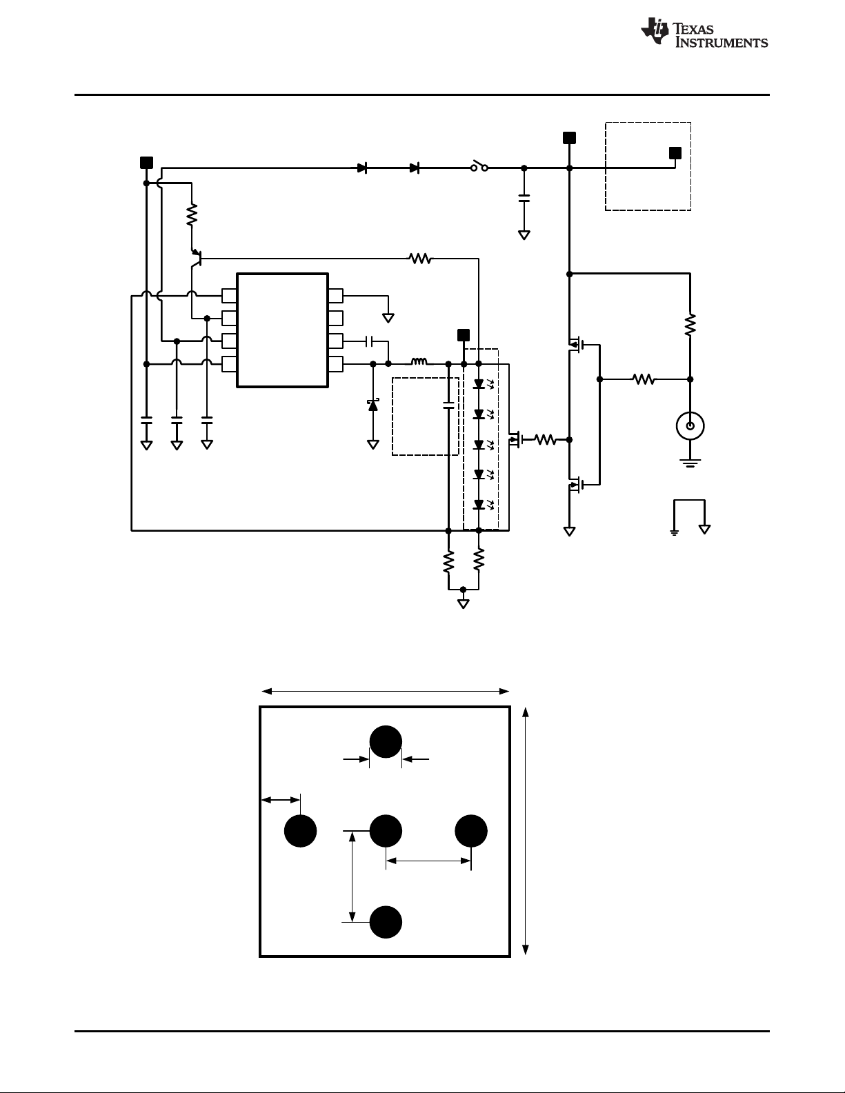
The PSOP-8 package is pin-for-pin compatible with the SO-8 package with the exception of the thermal
pad, or exposed die attach pad (DAP). The DAP is electrically connected to system ground. When the
DAP is properly soldered to an area of copper on the top layer, bottom layer, internal planes, or
combinations of various layers, the θJAof the LM3404/04HV can be significantly lower than that of the SO8 package. The PSOP-8 evaluation board is two layers of 1oz copper each, and measures 1.25" x 1.95".
The DAP is soldered to approximately 1/2 square inch of top and two square inches of bottom layer
copper. Three thermal vias connect the DAP to the bottom layer of the PCB. A recommended DAP/via
layout is shown in Figure 2.
All trademarks are the property of their respective owners.
SNVA342E–July 2008–Revised April 2013 AN-1839 LM3402/LM3404 Fast Dimming and True Constant LED Current
Submit Documentation Feedback
Copyright © 2008–2013, Texas Instruments Incorporated
Evaluation Board
1
Page 2
90 mil
10 mil
35 mil
10 mil
35 mil
90 mil
2
1
3
4
C1
V
IN
V
OUT
7
8
6
5
SW
BOOT
GND
DIM
VIN
VCC
RON
CS
C3
R1A
Q1
Q4
L1
R3
LEDs on separate PCB
Optional
R5
Q3
2
CONN-1
C4
V
DIM
C6
JMP-1
U1
External Voltage
Source Optional
4V to 6V
Single package (SC70-6)
Complementary N+P Channel
D1
D2
C2
C5
LM3404
R2
Q3
1
R1B
R4
R6
V
DIM
1N4148
Dual
Thermal Performance
www.ti.com
Figure 1. LM3402 / 04 Schematic
Figure 2. LM3402/04 PSOP Thermal PAD and Via Layout
2
AN-1839 LM3402/LM3404 Fast Dimming and True Constant LED Current SNVA342E–July 2008–Revised April 2013
Evaluation Board
Copyright © 2008–2013, Texas Instruments Incorporated
Submit Documentation Feedback
Page 3
L
T
S
DT
S
t
I
LED(t)
I
F
V
OUT
L
VIN - V
OUT
'i
L
D =
t
ON
t
ON
+ t
OFF
=
= tON x f
SW
t
ON
T
S
www.ti.com
4 Connecting to LED Array
The LM3402/04 evaluation board includes two standard 94 mil turret connectors for the cathode and
anode connections to a LED array.
5 Low Power Shutdown
The LM3402/04 can be placed into a low power shutdown state (IQtypically 90 µA) by grounding the DIM
terminal. During normal operation this terminal should be left open-circuit.
6 Constant On Time Overview
The LM3402 and LM3404 are buck regulators with a wide input voltage range and a low voltage
reference. The controlled on-time (COT) architecture is a combination of hysteretic mode control and a
one-shot on-timer that varies inversely with input voltage. With the addition of a PNP transistor, the ontimer can be made to be inversely proportional to the input voltage minus the output voltage. This is one of
the application improvements made to this demonstration board that will be discussed later (improved
average LED current circuit).
The LM3402 / 04 were designed with a focus of controlling the current through the load, not the voltage
across it. A constant current regulator is free of load current transients, and has no need for output
capacitance to supply the load and maintain output voltage. Therefore, in this demonstration board in
order to demonstrate the fast transient capabilities, I have chosen to omit the output capacitor. With any
Buck regulator, duty cycle (D) can be calculated with the following equations.
Connecting to LED Array
The average inductor current equals the average LED current whether an output capacitor is used or not.
Figure 3. Buck Converter Inductor Current Waveform
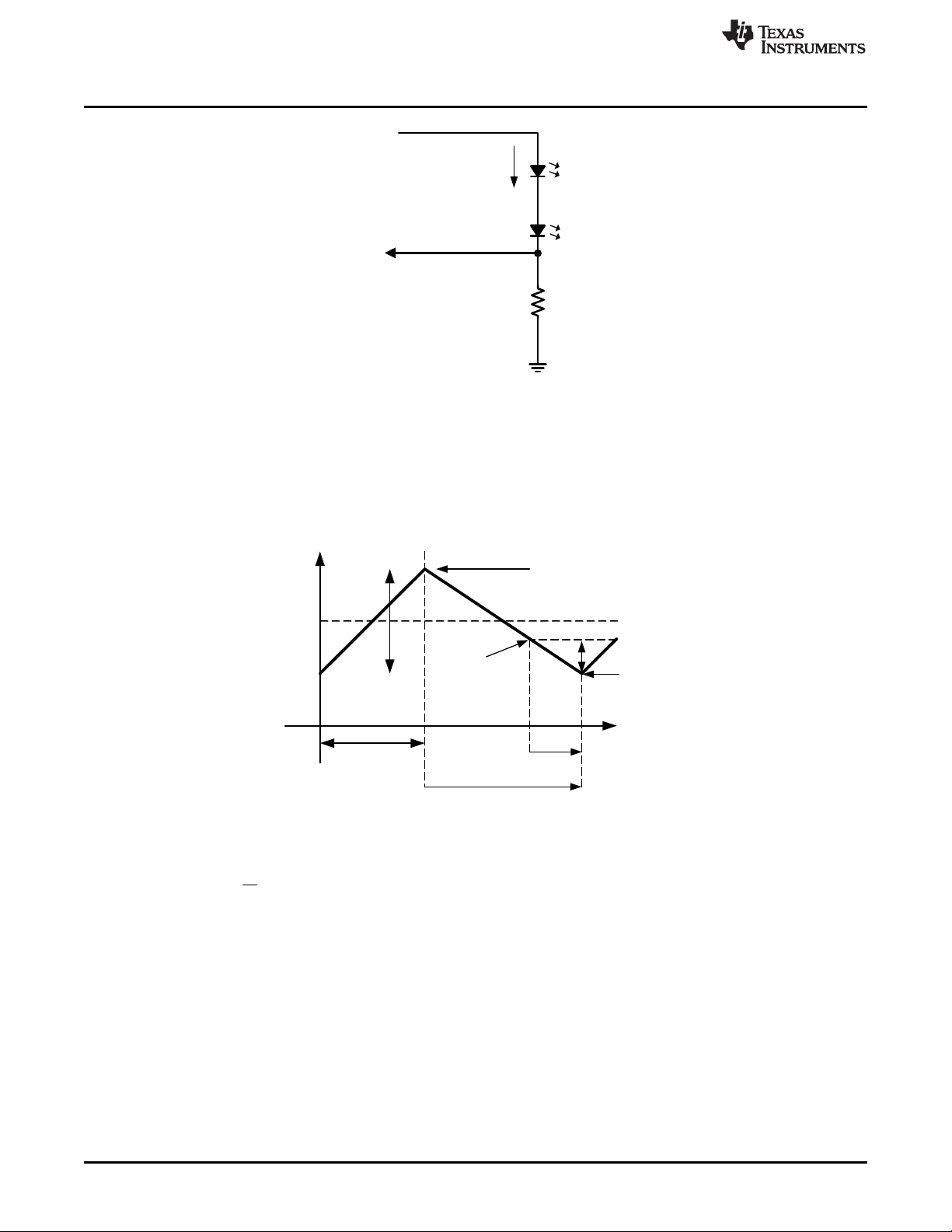
A voltage signal, V
ground. V
is fed back to the CS pin, where it is compared against a 200 mV reference (V
SNS
comparator turns on the power MOSFET when V
, is created as the LED current flows through the current setting resistor, R
SNS
falls below V
SNS
. The power MOSFET conducts for a
REF
REF
). A
SNS
, to
controlled on-time, tON, set by an external resistor, RON.
(1)
SNVA342E–July 2008–Revised April 2013 AN-1839 LM3402/LM3404 Fast Dimming and True Constant LED Current
Submit Documentation Feedback
3
Copyright © 2008–2013, Texas Instruments Incorporated
Evaluation Board
Page 4
I
LED-MIN
= IF -
'i
L
2
t
I
LED(t)
i
PEAK
t
ON
I
F
'i
D
'i
L
i
TARGET
i
LED-MIN
t
OFF
t
D
R
SNS
V
SNS
C
S
I
LED
+
-
Constant On Time Overview
www.ti.com
6.1 Setting the Average LED Current
Knowing the average LED current desired and the input and output voltages, the slopes of the currents
within the inductor can be calculated. The first step is to calculate the minimum inductor current (LED
current) point. This minimum level needs to be determined so that the average LED current can be
determined.
Figure 5. I
Figure 4. V
Current Waveform
SENSE
SNS
Circuit
Using Figure 3 and Figure 5 and the equations of a line, calculate I
LED-MIN
.
(2)
4
AN-1839 LM3402/LM3404 Fast Dimming and True Constant LED Current SNVA342E–July 2008–Revised April 2013
Evaluation Board
Copyright © 2008–2013, Texas Instruments Incorporated
Submit Documentation Feedback
Page 5

tON = k x
R
ON
V
IN
R
SNS
=
VIN - V
OUT
2L
x tON +
V
OUT
x t
D
L
(IF) -
0.20V
0.2V = R
SNS
VIN - V
OUT
2L
x tON +
V
OUT
L
x t
D
IF -
i
TARGET
= IF -
VIN - V
OUT
2L
x tON +
V
OUT
L
x t
D
V
OUT
L
'iD =
t
D
I
TARGET
= IF -
'i
L
2
+'i
D
=
VIN - V
OUT
2L
'i
2
x t
ON
www.ti.com
Where
The delta of the inductor current is given by:
There is a 220 ns delay (tD) from the time that the current sense comparator trips to the time at which the
control MOSFET actually turns on. We can solve for i
ΔiDis the magnitude of current beyond the target current and equal to:
Therefore:
The point at which you want the current sense comparator to give the signal to turn on the FET equals:
Therefore:
IF= I
i
TARGET
LED-Average
x R
SNS
Standard On-Time Set Calculation
(3)
(4)
knowing there is a delay.
TARGET
(5)
(6)
(7)
= 0.20V (8)
Finally R
can be calculated.
SNS
7 Standard On-Time Set Calculation
The control MOSFET on-time is variable, and is set with an external resistor RON(R2 from Figure 1). Ontime is governed by the following equation:
Where
k = 1.34 x 10
At the conclusion of tONthe control MOSFET turns off for a minimum OFF time (t
once t
OFF-MIN
The LM3402/04 have minimum ON and OFF time limitations. The minimum on time (tON) is 300 ns, and
the minimum allowed off time (t
Designing for the highest switching frequency possible means that you will need to know when minimum
ON and OFF times are observed.
Minimum OFF time will be seen when the input voltage is at its lowest allowed voltage, and the output
voltage is at its maximum voltage (greatest number of series LEDs).
The opposite condition needs to be considered when designing for minimum ON time. Minimum ON time
is the point at which the input voltage is at its maximum allowed voltage, and the output voltage is at its
lowest value.
-10
is complete the CS comparator compares V
) is 300 ns.
OFF
SNS
and V
) of 300 ns, and
again, waiting to begin the next cycle.
REF
OFF-MIN
(9)
(10)
(11)
(12)
SNVA342E–July 2008–Revised April 2013 AN-1839 LM3402/LM3404 Fast Dimming and True Constant LED Current
Submit Documentation Feedback
Copyright © 2008–2013, Texas Instruments Incorporated
Evaluation Board
5
Page 6

Application Circuit Calculations
8 Application Circuit Calculations
To better explain the improvements made to the COT LM3402/04 demonstration board, a comparison is
shown between the unmodified average output LED current circuit to the improved circuit. Design
Examples 1 and 2 use two original LM3402 / 04 circuits. The switching frequencies will be maximized to
provide a small solution size.
Design Example 3 is an improved average current application. Example 3 will be compared against
example 2 to illustrate the improvements.
Example 4 will use the same conditions and circuit as example 3, but the switching frequency will be
reduced to improve efficiency. The reduced switching frequency can further reduce any variations in
average LED current with a wide operating range of series LEDs and input voltages.
Design Example 1
• VIN= 48V (±20%)
• Driving three HB LEDs with VF= 3.4V
• V
• IF= 500 mA (typical application)
• Estimated efficiency = 82%
• fSW= fast as possible
• Design for typical application within tONand t
LED (inductor) ripple current of 10% to 60% is acceptable when driving LEDs. With this much allowed
ripple current, you can see that there is no need for an output capacitor. Eliminating the output capacitor is
actually desirable. An LED connected to an inductor without a capacitor creates a near perfect current
source, and this is what we are trying to create.
In this design we will choose 50% ripple current.
ΔiL= 500 mA x 0.50 = 250 mA
I
PEAK
Calculate tON, t
From the datasheet there are minimum control MOSFET ON and OFF times that need to be met.
t
OFF
tONminimum = 300 ns
The minimum ON time will occur when VINis at its maximum value. Therefore calculate RONat VIN= 60V,
and set tON= 300 ns.
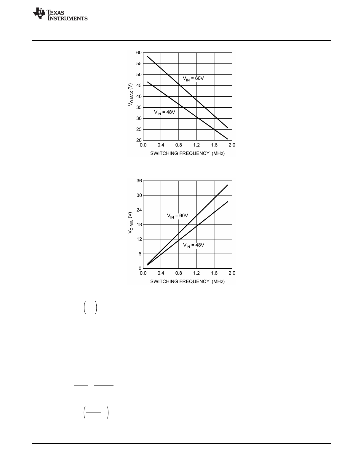
A quick guideline for maximum switching frequency allowed versus input and output voltages are in
Figure 6 and Figure 7.
= (3 x 3.4V +200 mV) = 10.4V
OUT
= 500 mA + 125 mA = 625 mA
and R
OFF
ON
minimum = 300 ns
limitations
OFF
www.ti.com
6
AN-1839 LM3402/LM3404 Fast Dimming and True Constant LED Current SNVA342E–July 2008–Revised April 2013
Evaluation Board
Copyright © 2008–2013, Texas Instruments Incorporated
Submit Documentation Feedback
Page 7
V
OUT
V
IN
x K
t
OFF
= t
ON
- 1
D =
V
OUT
V
IN
x K
=
t
ON
t
ON
+ t
OFF
tON = k x
R
ON
V
IN
www.ti.com
Application Circuit Calculations
Figure 6. V
Figure 7. V
OUT-MAX
OUT-MIN
vs f
vs f
SW
SW
RON= 135 kΩ (use standard value of 137 kΩ)
tON= 306 ns
Check to see if t
minimum is satisfied. This occurs when VINis at its minimum value.
OFF
At VIN= 36V, and RON= 137 kΩ calculate tONfrom previous equation.
tON= 510 ns
(13)
We know that:
Rearranging the above equation and solving for t
t
= 938 ns (satisfied)
OFF
SNVA342E–July 2008–Revised April 2013 AN-1839 LM3402/LM3404 Fast Dimming and True Constant LED Current
Submit Documentation Feedback
Copyright © 2008–2013, Texas Instruments Incorporated
with tONset to 510 ns
OFF
(14)
(15)
7
Evaluation Board
Page 8
I
LED(t)
i
PEAK
t
ON
I
F
'i
L
i
LED-MIN
t
OFF
t
Application Circuit Calculations
VIN(V) V
36 10.4 5.10E-07 9.38E-07
48 10.4 3.82E-07 1.06E-06
60 10.4 3.06E-07 1.14E-06
Calculate Switching Frequency
VIN= 36V, 48 and 60V.
Substituting equations:
fSW= 691kHz (VIN= 36V, 48V, and 60V)
Calculate Inductor Value
With 50% ripple at VIN= 48V
• IF= 500 mA
• ΔiL= 250 mA (target)
• L = 57 µH (68 µH standard value)
Calculate Δi for VIN= 36V, 48V, and 60V with L = 68 µH
VIN(V) V
36 10.4 0.192
48 10.4 0.211
60 10.4 0.223
Table 1. Example 1 ON and OFF Times
(V) t
OUT
ON
Table 2. Example 1 Ripple Current
(V) ΔiL(A)
OUT
t
OFF
www.ti.com
Calculate R
Calculate R
SNS
at VINtypical (48V), and average LED current (IF) set to 500 mA.
SNS
Figure 8. Inductor Current Waveform
• IF= 500 mA
• VIN= 48V
• V
• L = 68 µH
• tD= 220 ns
• tON= 382 ns
Using equations from the COT Overview section, calculate R
8
AN-1839 LM3402/LM3404 Fast Dimming and True Constant LED Current SNVA342E–July 2008–Revised April 2013
Evaluation Board
OUT
= 10.4V
.
SNS
Copyright © 2008–2013, Texas Instruments Incorporated
Submit Documentation Feedback
Page 9

tON = k x
R
ON
V
IN
IF =
R
SNS
0.20V
+
VIN - V
OUT
2L
(tON) -
V
OUT
x t
D
L
R
SNS
=
VIN - V
OUT
2L
x tON +
V
OUT
x t
D
L
(IF) -
0.20V
R
SNS
=
VIN - V
OUT
2L
V
OUT
x t
D
L
(IF) -
0.20V
Or:
k x R
ON
V
IN
+
www.ti.com
Therefore: R
Calculate Average LED current (IF)
Calculate average current through the LEDs for VIN= 36V and 60V.
Design Example 2
Design example 2 demonstrates a design if a single Bill of Materials (Bom) is desired over many different
applications (number of series LEDs, VIN, V
• VIN= 48V (±20%)
• Driving 3, 4, or 5 HB LEDs with VF= 3.4V
• IF= 500 mA (typical application)
• Estimated efficiency = 82%
• fSW= fast as possible
• Design for typical application within tONand t
The inductor, RONresistor, and the R
• V
• V
• V
Calculate tON, t
In this design we will maximize the switching frequency so that we can reduce the overall size of the
design. In a later design, a slower switching frequency is utilized to maximize efficiency. If the design is to
use the highest possible switching frequency, you must ensure that the minimum on and off times are
adhered to.
Minimum on time occurs when VINis at its maximum value, and V
Calculate RONat VIN= 60V, V
= 467 mΩ
SNS
VIN(V) V
36 10.4 0.490
48 10.4 0.500
60 10.4 0.506
= 3 x 3.4V + 200 mV = 10.4V
OUT
= 4 x 3.4V + 200 mV = 13.8V
OUT
= 5 x 3.4V + 200 mV = 17.2V
OUT
and R
OFF
ON
Table 3. Example 1 Average LED Current
(V) IF(A)
OUT
etc).
OUT
limitations
OFF
resistor is calculated for a typical or average design.
SNS
is at its lowest value.
OUT
= 10.4V, and set tON= 300 ns:
OUT
Application Circuit Calculations
(16)
(17)
RON= 137 kΩ, tON= 306 ns
Check to see if t
t
minimum occurs when VINis at its lowest value, and V
SNVA342E–July 2008–Revised April 2013 AN-1839 LM3402/LM3404 Fast Dimming and True Constant LED Current
Submit Documentation Feedback
OFF
At VIN= 36V, V
minimum is satisfied:
OFF
is at its maximum value.
= 17.2V, and RON= 137 kΩ calculate tONfrom the above equation:
OUT
Copyright © 2008–2013, Texas Instruments Incorporated
OUT
(18)
9
Evaluation Board
Page 10

'i
V
IN
- V
OUT
L =
x t
ON
fSW =
1
tON + t
OFF
fSW =
V
OUT
K x k x R
ON
fSW =
V
OUT
VIN x K x t
ON
V
OUT
V
IN
x K
t
OFF
= t
ON
- 1
V
OUT
V
IN
x K
=
t
ON
t
ON
+ t
OFF
Application Circuit Calculations
tON= 510 ns
Rearrange the above equation and solve for t
t
= 365 ns (satisfied)
OFF
Three Series LEDs
VIN(V) V
36 10.4 137 kΩ 5.10E-07 9.38E-07
48 10.4 137 kΩ 3.82E-07 1.06E-06
60 10.4 137 kΩ 3.06E-07 1.14E-06
Four Series LEDs
36 13.8 137 kΩ 5.10E-07 5.81E-07
48 13.8 137 kΩ 3.82E-07 7.08E-07
60 13.8 137 kΩ 3.06E-07 7.85E-07
Five Series LEDs
36 17.2 137 kΩ 5.10E-07 3.65E-07
48 17.2 137 kΩ 3.82E-07 4.93E-07
60 17.2 137 kΩ 3.06E-07 5.69E-07
with tONset to 510 ns
OFF
Table 4. Example 2 On and Off Time
(V) R
OUT
ON
www.ti.com
(19)
(20)
t
ON
t
OFF
Calculate Switching Frequency
The switching frequency will only change with output voltage.
Substituting equations:
Or:
• fSW= 691 kHz (V
• fSW= 916 kHz (V
• fSW= 1.14 MHz (V
OUT
OUT
OUT
= 10.4V)
= 13.8V)
= 17.2V)
Calculate Inductor Value
With 50% ripple at VIN= 48V, and V
• I
= 500 mA
AVG
OUT
= 10.4V
• ΔiL= 250 mA (target)
• L = 53 µH (68 uH standard value)
(21)
(22)
(23)
(24)
Calculate Δi for VIN= 36V, 48V, and 60V with L = 68 µH.
10
AN-1839 LM3402/LM3404 Fast Dimming and True Constant LED Current SNVA342E–July 2008–Revised April 2013
Evaluation Board
Copyright © 2008–2013, Texas Instruments Incorporated
Submit Documentation Feedback
Page 11

IF =
R
SNS
0.20V
+
VIN - V
OUT
2L
(tON) -
V
OUT
x t
D
L
R
SNS
=
VIN - V
OUT
2L
x tON +
V
OUT
x t
D
L
(IF) -
0.20V
www.ti.com
Three Series LEDs
Four Series LEDs
Four Series LEDs
Application Circuit Calculations
Table 5. Example 2 Ripple Current
VIN(V) V
36 10.4 0.192
48 10.4 0.211
60 10.4 0.223
36 13.8 0.166
48 13.8 0.192
60 13.8 0.208
36 17.2 0.141
48 17.2 0.173
60 17.2 0.193
(V) ΔiL(A)
OUT
Calculate R
Calculate R
SNS
at VINtypical (48V), with four series LEDs (13.8V = V
SNS
to 500 mA.
• IF= 500 mA
• VIN= 48V
• V
OUT
= 13.8V
• L = 68 µH
• tD= 220 ns
• tON= 382 ns
R
= 446 mΩ
SNS
Calculate Average Current through LED
All combinations of VIN, V
OUT
with R
= 446 mΩ
SNS
Table 6. Example 2 Average LED Current
VIN(V) V
Three Series LEDs
36 10.4 0.511
48 10.4 0.521
60 10.4 0.526
Four Series LEDs
36 13.8 0.487
48 13.8 0.500
60 13.8 0.508
Five Series LEDs
36 17.2 0.463
48 17.2 0.479
60 17.2 0.489
), and average LED current (IF) set
OUT
(V) IF(A)
OUT
(25)
(26)
SNVA342E–July 2008–Revised April 2013 AN-1839 LM3402/LM3404 Fast Dimming and True Constant LED Current
Submit Documentation Feedback
Copyright © 2008–2013, Texas Instruments Incorporated
Evaluation Board
11
Page 12

V
OUT
V
IN
x K
t
OFF
= t
ON
- 1
VIN - V
OUT
k
R
ON
= t
ON
VIN - V
OUT
R
ON
t
ON
= k x
Modified COT Application Circuit
In this application you can see that there is a difference of 63 mA between the low and high of the
average LED current.
9 Modified COT Application Circuit
With the addition of one pnp transistor and one resistor (Q1 and R3) the average current through the
LEDs can be made to be more constant over input and output voltage variations. Refer to page one,
Figure 1. Resistor RON(R2) and Q1 turn the tONequation into:
Ignore the PNP transistor’s VBEvoltage drop.
Design to the same criteria as the previous example with the improved application and compare results.
10 Modified Application Circuit Design Example 3
Design Example 1
• VIN= 48V (±20%)
• Driving 3, 4, or 5 HB LEDs with VF= 3.4V
• IF= 500 mA (typical application)
• Estimated efficiency = 82%
• fSW= fast as possible
• Design for typical application within tONand t
The inductor, RONresistor, and the R
• V
= 3 x 3.4V + 200 mV = 10.4V
OUT
• V
= 4 x 3.4V + 200 mV = 13.8V
OUT
• V
= 5 x 3.4V + 200 mV = 17.2V
OUT
Calculate tON, t
OFF
and R
ON
resistor are calculated for a typical or average design.
SNS
Minimum ON time occurs when VINis at its maximum value, and V
Calculate RONat VIN= 60V, V
= 10.4V, and set tON= 300 ns:
OUT
limitations
OFF
is at its lowest value.
OUT
www.ti.com
(27)
12
RON= 111 kΩ (113 kΩ) tON= 306 ns
Check to see if t
At VIN= 36V, V
minimum is satisfied.
OFF
= 17.2V, and RON= 113 kΩ calculate t
OUT
ON:
.
tON= 806 ns
t
= 577 ns (satisfied)
OFF
AN-1839 LM3402/LM3404 Fast Dimming and True Constant LED Current SNVA342E–July 2008–Revised April 2013
Evaluation Board
Copyright © 2008–2013, Texas Instruments Incorporated
Submit Documentation Feedback
(28)
(29)
Page 13

2
1
3
4
7
8
6
5
C1
V
IN
V
OUT
SW
BOOT
GND
DIM
VIN
VCC
RON
CS
C3
Q1
L1
R3
LEDs on separate PCB
Optional
C4
U1
D1
C2
C5
LM3404
R2
R1
Improved Average
Current Circuit
www.ti.com
Modified Application Circuit Design Example 3
Figure 9. Improved Average LED Current Application Circuit
Table 7. Example 3 On and Off Times
Three Series LEDs
Four Series LEDs
Five Series LEDs
VIN(V) V
36 10.4 113 kΩ 5.92E-07 1.09E-07
48 10.4 113 kΩ 4.03E-07 1.12E-06
60 10.4 113 kΩ 3.06E-07 1.14E-06
36 13.8 113 kΩ 6.83E-07 7.78E-07
48 13.8 113 kΩ 4.43E-07 8.21E-07
60 13.8 113 kΩ 3.28E-07 8.41E-07
36 17.2 113 kΩ 8.06E-07 5.77E-07
48 17.2 113 kΩ 4.92E-07 6.34E-07
60 17.2 113 kΩ 3.54E-07 6.59E-07
(V) R
OUT
ON
t
ON
t
OFF
SNVA342E–July 2008–Revised April 2013 AN-1839 LM3402/LM3404 Fast Dimming and True Constant LED Current
Submit Documentation Feedback
Copyright © 2008–2013, Texas Instruments Incorporated
Evaluation Board
13
Page 14

R
SNS
=
VIN - V
OUT
2L
V
OUT
x t
D
L
(IF) -
0.20V
R
ON
VIN - V
OUT
+
k x
R
SNS
=
VIN - V
OUT
2L
x tON +
V
OUT
x t
D
L
(IF) -
0.20V
'i
R
ON
L =
x k
VIN - V
OUT
R
ON
t
ON
= k x
'i
V
IN
- V
OUT
L =
x t
ON
fSW =
V
OUT
VIN x K x t
ON
Or:
fSW =
1
tON + t
OFF
Modified Application Circuit Design Example 3
Calculate Switching Frequency
Table 8. Example 3 Switching Frequency
VIN(V) V
Three Series LEDs
36 10.4 595
48 10.4 656
60 10.4 692
Four Series LEDs
36 13.8 685
48 13.8 791
60 13.8 855
Five Series LEDs
36 17.2 723
48 17.2 888
60 17.2 987
(V) fSW(kHz)
OUT
www.ti.com
(30)
Calculate Inductor Value
Therefore:
You can quickly see one benefit of the modified circuit. The improved circuit eliminates the input and
output voltage variation on RMS current.
• IF= 500 mA (typical application)
• ΔiL= 250 mA (target)
• RON= 113 kΩ
• L = 59 µH (68 µH standard value)
• ΔiL= 223 mA (L = 68 µH all combinations)
Calculate R
Original R
SNS
equation:
SNS
Substitute improved circuit tONcalculation:
(31)
(32)
(33)
14
Simplified:
AN-1839 LM3402/LM3404 Fast Dimming and True Constant LED Current SNVA342E–July 2008–Revised April 2013
Evaluation Board
Copyright © 2008–2013, Texas Instruments Incorporated
Submit Documentation Feedback
(34)
Page 15

V
OUT
x t
D
L
+
0.20V
k x R
ON
2L
-
R
SNS
IF =
VIN - V
OUT
2L
V
OUT
x t
D
L
+
0.20V
k x R
ON
VIN - V
OUT
-
R
SNS
IF =
R
SNS
=
V
OUT
x t
D
L
(IF) -
0.20V
k x R
ON
2L
+
www.ti.com
Typical Application:
• V
• IF= 500 mA
• RON= 113 kΩ
• L = 68 µH
• tD= 220 ns
R
This equation shows that only variations in V
range. These variations should be very minor even with large variations in output voltage.
Calculate Average Current through LED
Modified application circuit average forward current equation.
Simplified:
OUT
= 462 mΩ
SNS
= 13.8V
Modified Application Circuit Design Example 4
will affect the average current over the entire application
OUT
(35)
(36)
(37)
Table 9. Example 3 Average LED Current
VIN(V) V
Three Series LEDs
36 10.4 0.511
48 10.4 0.511
60 10.4 0.511
Four Series LEDs
36 13.8 0.500
48 13.8 0.500
60 13.8 0.500
Five Series LEDs
36 17.2 0.489
48 17.2 0.489
60 17.2 0.489
OUT
In this application you can see that there is a difference of 22 mA between the low and high of the
average LED current.
11 Modified Application Circuit Design Example 4
• VIN= 48V (±20%)
• Driving 3, 4, or 5 HB LEDs with VF= 3.4V
• IF= 500 mA (typical application)
• Estimated efficiency = 82%
• fSW= 500 kHz (typ app)
(V) IF(A)
The inductor, RONresistor, and the R
• V
= 3 x 3.4V + 200 mV = 10.4V
OUT
SNVA342E–July 2008–Revised April 2013 AN-1839 LM3402/LM3404 Fast Dimming and True Constant LED Current
Submit Documentation Feedback
Copyright © 2008–2013, Texas Instruments Incorporated
resistor are calculated for a typical or average design.
SNS
Evaluation Board
15
Page 16

fSW =
V
OUT
VIN x K x t
ON
Or:
fSW =
1
tON + t
OFF
'i
R
ON
L =
x k
t
ON
k
R
ON
=
(V
IN
- V
OUT)
V
OUT
V
IN
x K
t
ON
=
1
f
SW
Modified Application Circuit Design Example 4
• V
= 4 x 3.4V + 200 mV = 13.8V
OUT
• V
= 5 x 3.4V + 200 mV = 17.2V
OUT
Reduce switching frequency for the typical application to about 500 kHz to increase efficiency.
Calculate tON, t
• V
OUT
= 13.8V
OFF
and R
ON
• VIN= 48V
• IF= 500 mA
• tD= 220 ns
• η = 0.85
• fSW= 500 kHz
tON≊ 705 ns
RON≊ 179 kΩ (use standard value of 182 kΩ)
Calculate Inductor Value
www.ti.com
(38)
(39)
• IF= 500 mA
• ΔiL= 250 mA (target)
• RON= 182 kΩ
• L = 100 µH
Calculate ΔiLwith L = 100 µH (VIN= 48V, V
OUT
= 13.8V)
ΔiL= 241 mA (all combinations)
Calculate Switching Frequency
Table 10. Example 4 Switching Frequency
VIN(V) V
Three Series LEDs
36 10.4 374
48 10.4 412
60 10.4 435
Four Series LEDs
36 13.8 430
48 13.8 497
60 13.8 537
Five Series LEDs
36 17.2 454
48 17.2 558
60 17.2 620
16
AN-1839 LM3402/LM3404 Fast Dimming and True Constant LED Current SNVA342E–July 2008–Revised April 2013
Evaluation Board
Copyright © 2008–2013, Texas Instruments Incorporated
(V) fSW(kHz)
OUT
Submit Documentation Feedback
(40)
(41)
Page 17

V
OUT
x t
D
L
+
0.20V
k x R
ON
2L
-
R
SNS
IF =
R
SNS
=
V
OUT
x t
D
L
(IF) -
0.20V
k x R
ON
2L
+
www.ti.com
Dimming
Calculate R
• V
OUT
SNS
= 13.8V
• VIN= 48V
• IF= 500 mA
• tD= 220 ns
• η = 0.85
• L = 100 µH
R
= 488 mΩ
SNS
Calculate Average Current through LED
Table 11. Example 4 Average LED Current
VIN(V) V
Three Series LEDs
36 10.4 0.507
48 10.4 0.507
60 10.4 0.507
Four Series LEDs
36 13.8 0.500
48 13.8 0.500
60 13.8 0.500
Five Series LEDs
36 17.2 0.493
48 17.2 0.493
60 17.2 0.493
(V) IF(A)
OUT
(42)
(43)
In the reduced frequency application you can see that there is a difference of 14 mA between the low and
high of the average current.
If the original tONcircuit was used (no PNP transistor) with the switching frequency centered around 500
kHz the difference between the high and low values would be about 67 mA.
12 Dimming
The DIM pin of the LM3402/04 is a TTL compatible input for low frequency pulse width modulation (PWM)
dimming of the LED current. Depending on the application, a contrast ratio greater than what the
LM3402/04 internal DIM circuitry can provide might be needed. This demonstration board comes with
external circuitry that allows for dimming contrast ratios greater than 50k:1.
13 LM3402/04 DIM Pin Operation
To fully enable and disable the LM3402 / 04, the PWM signal should have a maximum logic low level of
0.8V and a minimum logic high level of 2.2V. Dimming frequency, f
the LED current rise time and fall time and the delay from activation of the DIM pin to the response of the
internal power MOSFET. In general, f
should be at least one order of magnitude lower than the steady
DIM
state switching frequency in order to prevent aliasing.
SNVA342E–July 2008–Revised April 2013 AN-1839 LM3402/LM3404 Fast Dimming and True Constant LED Current
Submit Documentation Feedback
Copyright © 2008–2013, Texas Instruments Incorporated
, and duty cycle, D
DIM
, are limited by
DIM
Evaluation Board
17
Page 18

T
D
t
D
t
SD
tDtSUt
SD
tDt
SU
t
SD
D
MIN
D
MAX
T T
DIM
I
F
f
PWM
T =
1
T
tD + t
SU
D
MIN
=
T
T - t
SD
D
MAX
=
t
SU
Contrast Ratio Definition
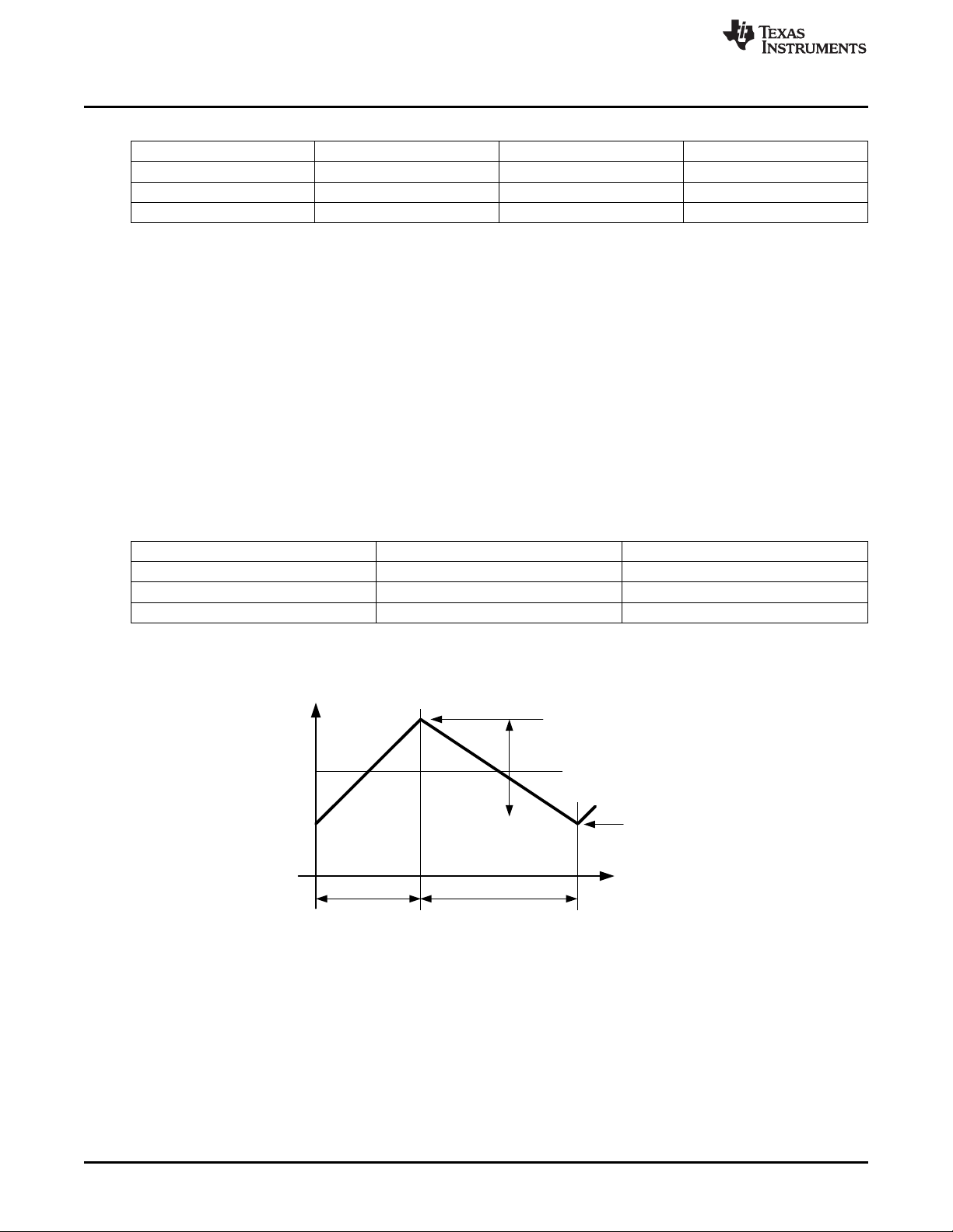
For illustrations, see Figure 10. The interval tDrepresents the delay from a logic high at the DIM pin to the
onset of the output current. The quantities tSUand tSDrepresent the time needed for the LED current to
slew up to steady state and slew down to zero, respectively.
As an example, assume a DIM duty cycle D
of current through the LED string. At D
through your LED string (250 mA). This could only be possible if there were no delays (tD) between the
on/off DIM signal and the on/off of the LED current. The rise and fall times (tSUand tSD) of the LED current
would also need to be eliminated. If we can reduce these times, the linearity between the PWM signal and
the average current will be realized.
equal to 100% (always on) and the circuit delivers 500mA
DIM
equal to 50% you would like exactly ½ of 500 mA of current
DIM
www.ti.com
Figure 10. Contrast Ratio Definitions
14 Contrast Ratio Definition
Contrast Ratio (CR) = 1/D
D
= (tD+ tSU) x f
MIN
DIM
MIN
18
AN-1839 LM3402/LM3404 Fast Dimming and True Constant LED Current SNVA342E–July 2008–Revised April 2013
Evaluation Board
Copyright © 2008–2013, Texas Instruments Incorporated
Submit Documentation Feedback
Page 19

2 Ps/DIV
I
F
200 mA/Div
DIM
5V/Div
www.ti.com
Figure 11. tDand tSU(DIM Pin)
15 External MOSFET Dimming and Contrast Ratio
MOSFET Q4 and its drive circuitry are provided on the demonstration PCB (see Figure 12). When
MOSFET Q4 is turned on, it shorts LED+ to LED-, therefore redirecting the inductor current from the LED
string to the shunt MOSFET. The LM3402 / 04 is never turned off, and therefore become a perfect current
source by providing continuous current to the output through the inductor (L1). A buck converter with an
external shunt MOSFET is the ideal circuit for delivering the highest possible contrast ratio. For typical
delays and rise time for external MOSFET dimming, see Figure 13 - Figure 15.
External MOSFET Dimming and Contrast Ratio
SNVA342E–July 2008–Revised April 2013 AN-1839 LM3402/LM3404 Fast Dimming and True Constant LED Current
Submit Documentation Feedback
Copyright © 2008–2013, Texas Instruments Incorporated
Evaluation Board
19
Page 20

8.0 0.0 8.4 16.6 24.8 33.0
V
DIM
(V)
TIME (Ps)
-1.0
2.0
5.0
8.0
11.0
I
LED
(
A
)
-0.1
0.2
0.5
0.8
1.1
I
LED
V
DIM
R1A
Q4
L1
LEDs on separate PCB
Optional
R5
Q3
2
CONN-1
C4
V
DIM
C5
JMP-1
External Voltage
Source Optional
4V to 6V
1N4148
Dual
Single package (SC70-6)
Complementary N+P Channel
D2
Q3
1
R1B
R4
R6
V
DIM
From V
CC
LM3402/04
External MOSFET Dimming and Contrast Ratio
www.ti.com
Figure 12. VIN= 24V, 3 series LEDs @ 400mA
AN-1839 LM3402/LM3404 Fast Dimming and True Constant LED Current SNVA342E–July 2008–Revised April 2013
Evaluation Board
20
Copyright © 2008–2013, Texas Instruments Incorporated
Submit Documentation Feedback
Page 21

VIN - 0.2V
R
ON
t
ON
= k x
VIN - V
OUT
R
ON
t
ON
= k x
TIME (ns)
-100
-60 -20 20 60
100
V
DIM
(V)
I
LED
(
A
)
-0.20
0.20
0.60
1.00
0.0
4.0
8.0
12.0
I
LED
V
DIM
36 ns
TIME (ns)
-100
-60 -20 20 60
100
V
DIM
(V)
I
LED
(
A
)
-0.1
0.2
0.5
0.8
1.1
-1
3
7
11
I
LED
V
DIM
40 ns
www.ti.com
Fast Dimming + Improved Average Current Circuit
Figure 13. tD+ tSUGraph
Figure 14. tD+ tSDGraph
16 Fast Dimming + Improved Average Current Circuit
Using both the Improved Average LED current circuit and the external MOSFET fast dimming circuit
together has additional benefits. If RONand the converter's switching frequency (fSW) is determined and set
with the improved average LED current circuit, the switching frequency will decrease once V
during fast dimming. With MOSFET Q4 on, V
is equal to VFB(200 mV). The tONequation then becomes
OUT
almost identical to the original unmodified circuit equation.
Setting tONand RON:
tONequation becomes:
when Q4 shunt MOSFET is on during fast dimming.
t
OFF
SNVA342E–July 2008–Revised April 2013 AN-1839 LM3402/LM3404 Fast Dimming and True Constant LED Current
Submit Documentation Feedback
equation during normal operation is:
Copyright © 2008–2013, Texas Instruments Incorporated
Evaluation Board
is shorted
OUT
(44)
(45)
21
Page 22

0 10 20 30 40 50 60 70 80 90 100
0
50
100
150
200
250
350
I
LED
(A)
DUTY CYCLE (%)
300
f
DIM
= 25 kHz
f
DIM
= 5 kHz
f
DIM
= 500 Hz
-6.0
0.5 7.0 13.5 20.0
TIME (Ps)
-2.0
4.0
10.0
16.0
22.0
28.0
34.0
V
SW
(V)
0.5
0.4
0.2
0.1
-0.1
-0.3
-0.4
I
LED
(
A
)
fSW = 650 kHz
I
LED
(A)
VSW (V)
V
DIM
(V)
fSW = 75 kHz
0.2V
V
IN
x K
t
OFF
= t
ON
- 1
V
OUT
V
IN
x K
t
OFF
= t
ON
- 1
Linearity with Fast Dimming
t
equation then becomes:
OFF
when Q2 shunt MOSFET is OFF during fast dimming.
This is an added benefit due to the fact that t
frequency is decreased, which leads to improved efficiency (see Figure 16). Inductor L1 still remains
charged, and as soon as Q4 turns off current flows through the LED string.
is greatly increased, and therefore the switching
OFF
www.ti.com
(46)
(47)
17 Linearity with Fast Dimming
Once the delays and rise/fall times have been greatly reduced, linear average current vs, duty cycle (D
can be achieved at very high dimming frequencies (f
22
AN-1839 LM3402/LM3404 Fast Dimming and True Constant LED Current SNVA342E–July 2008–Revised April 2013
Evaluation Board
Figure 15. Improved Avg I
Figure 16. Linearity With Fast Dimming
Copyright © 2008–2013, Texas Instruments Incorporated
Circuit + Fast Dimming
LED
) (see Figure 17).
DIM
DIM
Submit Documentation Feedback
)
Page 23

2
1
3
4
C1
V
IN
V
OUT
7
8
6
5
SW
BOOT
GND
DIM
VIN
VCC
RON
CS
C3
R1A
Q1
Q4
L1
R3
LEDs on separate PCB
Optional
R5
Q3
2
CONN-1
C4
V
DIM
C6
JMP-1
U1
External Voltage
Source Optional
4V to 6V
Single package (SC70-6)
Complementary N+P Channel
D1
D2
C2
C5
LM3404
R2
Q3
1
R1B
R4
R6
V
DIM
1N4148
Dual
www.ti.com
LM3404 Improved ILED Average and Fast Dimming Demonstration Board
18 LM3404 Improved ILED Average and Fast Dimming Demonstration Board
Figure 17. VIN= 9V to 18V, I
= 700 mA, 3 x 3.4V White LED Strings (fSW≊≊ 500 kHz)
LED
SNVA342E–July 2008–Revised April 2013 AN-1839 LM3402/LM3404 Fast Dimming and True Constant LED Current
Submit Documentation Feedback
Copyright © 2008–2013, Texas Instruments Incorporated
Evaluation Board
23
Page 24

Bill of Materials
19 Bill of Materials
Part ID Part Value Mfg Part Number
U1 1A Buck LED Driver NSC LM3404
C1, Input Cap 10 µF, 25V, X5R TDK C3225X5R1E106M
C2, C6 Cap 1 µF, 16V, X5R TDK C1608X5R1C105M
C3, V
C4 Output Cap 10 µF, 25V, X5R (Optional) TDK C3225X5R1E106M
C5, V
D1, Catch Diode 0.5VfSchottky 2A, 30V
R1A, R1B 0.62Ω 1% 0.25W 1206 ROHM MCR18EZHFLR620
Test Points Connector Keystone 1502-2
VIN, GND, LED+, LED- Connector Keystone 575-8
Cap 0.1 µF, X5R TDK C1608X5R1H104M
BOOST
Cap 0.01 µF, X5R TDK C1608X5R1H103M
RON
D2 Dual SMT small signal Diodes INC BAV199
L1 33 µH CoilCraft D01813H-333
R2 47.5 kΩ 1% Vishay CRCW08054752F
R3 1.0 kΩ, 1% Vishay CRCW08051001F
R4, R5 1Ω, 1% Vishay CRCW08051R00F
R6 10 kΩ, 1% Vishay CRCW08051002F
Q1 SOT23 PNP Diodes INC MMBT3906
Q4 SOT23-6 N-CH 2.4A, 20V ZETEX ZXMN2A01E6
Q3 SC70-6, P + N Channel Vishay Si1539DL
JMP-1 Jumper Molex 22-28-4023
J15 50Ω BNC Amphenol 112538
SO PowerPAD pkg
www.ti.com
R
Diodes INC B230
20 Layout
24
AN-1839 LM3402/LM3404 Fast Dimming and True Constant LED Current SNVA342E–July 2008–Revised April 2013
Evaluation Board
Copyright © 2008–2013, Texas Instruments Incorporated
Submit Documentation Feedback
Page 25

IMPORTANT NOTICE
Texas Instruments Incorporated and its subsidiaries (TI) reserve the right to make corrections, enhancements, improvements and other
changes to its semiconductor products and services per JESD46, latest issue, and to discontinue any product or service per JESD48, latest
issue. Buyers should obtain the latest relevant information before placing orders and should verify that such information is current and
complete. All semiconductor products (also referred to herein as “components”) are sold subject to TI’s terms and conditions of sale
supplied at the time of order acknowledgment.
TI warrants performance of its components to the specifications applicable at the time of sale, in accordance with the warranty in TI’s terms
and conditions of sale of semiconductor products. Testing and other quality control techniques are used to the extent TI deems necessary
to support this warranty. Except where mandated by applicable law, testing of all parameters of each component is not necessarily
performed.
TI assumes no liability for applications assistance or the design of Buyers’ products. Buyers are responsible for their products and
applications using TI components. To minimize the risks associated with Buyers’ products and applications, Buyers should provide
adequate design and operating safeguards.
TI does not warrant or represent that any license, either express or implied, is granted under any patent right, copyright, mask work right, or
other intellectual property right relating to any combination, machine, or process in which TI components or services are used. Information
published by TI regarding third-party products or services does not constitute a license to use such products or services or a warranty or
endorsement thereof. Use of such information may require a license from a third party under the patents or other intellectual property of the
third party, or a license from TI under the patents or other intellectual property of TI.
Reproduction of significant portions of TI information in TI data books or data sheets is permissible only if reproduction is without alteration
and is accompanied by all associated warranties, conditions, limitations, and notices. TI is not responsible or liable for such altered
documentation. Information of third parties may be subject to additional restrictions.
Resale of TI components or services with statements different from or beyond the parameters stated by TI for that component or service
voids all express and any implied warranties for the associated TI component or service and is an unfair and deceptive business practice.
TI is not responsible or liable for any such statements.
Buyer acknowledges and agrees that it is solely responsible for compliance with all legal, regulatory and safety-related requirements
concerning its products, and any use of TI components in its applications, notwithstanding any applications-related information or support
that may be provided by TI. Buyer represents and agrees that it has all the necessary expertise to create and implement safeguards which
anticipate dangerous consequences of failures, monitor failures and their consequences, lessen the likelihood of failures that might cause
harm and take appropriate remedial actions. Buyer will fully indemnify TI and its representatives against any damages arising out of the use
of any TI components in safety-critical applications.
In some cases, TI components may be promoted specifically to facilitate safety-related applications. With such components, TI’s goal is to
help enable customers to design and create their own end-product solutions that meet applicable functional safety standards and
requirements. Nonetheless, such components are subject to these terms.
No TI components are authorized for use in FDA Class III (or similar life-critical medical equipment) unless authorized officers of the parties
have executed a special agreement specifically governing such use.
Only those TI components which TI has specifically designated as military grade or “enhanced plastic” are designed and intended for use in
military/aerospace applications or environments. Buyer acknowledges and agrees that any military or aerospace use of TI components
which have not been so designated is solely at the Buyer's risk, and that Buyer is solely responsible for compliance with all legal and
regulatory requirements in connection with such use.
TI has specifically designated certain components as meeting ISO/TS16949 requirements, mainly for automotive use. In any case of use of
non-designated products, TI will not be responsible for any failure to meet ISO/TS16949.
Products Applications
Audio www.ti.com/audio Automotive and Transportation www.ti.com/automotive
Amplifiers amplifier.ti.com Communications and Telecom www.ti.com/communications
Data Converters dataconverter.ti.com Computers and Peripherals www.ti.com/computers
DLP® Products www.dlp.com Consumer Electronics www.ti.com/consumer-apps
DSP dsp.ti.com Energy and Lighting www.ti.com/energy
Clocks and Timers www.ti.com/clocks Industrial www.ti.com/industrial
Interface interface.ti.com Medical www.ti.com/medical
Logic logic.ti.com Security www.ti.com/security
Power Mgmt power.ti.com Space, Avionics and Defense www.ti.com/space-avionics-defense
Microcontrollers microcontroller.ti.com Video and Imaging www.ti.com/video
RFID www.ti-rfid.com
OMAP Applications Processors www.ti.com/omap TI E2E Community e2e.ti.com
Wireless Connectivity www.ti.com/wirelessconnectivity
Mailing Address: Texas Instruments, Post Office Box 655303, Dallas, Texas 75265
Copyright © 2013, Texas Instruments Incorporated
 Loading...