

Page 1

1 Introduction
The LM3431 is a combination switching boost voltage regulator and multi-channel LED current controller.
The LM3431 Evaluation Board is designed to drive four parallel strings of eight series LEDs at 140mA per
string from an input voltage range of 8V to 18V. The boost switcher regulates LED cathode voltage for
optimum efficiency, while allowing the output voltage to vary according to the LED forward voltage. The
LM3431 incorporates complete fault protection features including LED short and open protection, overcurrent protection, over-voltage and under-voltage protection, and thermal shutdown. The error detection
flag can be monitored at the DLY post, which has a programmable delay time.
The board includes a DIM input terminal for a selectable digital or analog dimming control signal. PWM
dimming frequencies up to 1kHz at 100:1 contrast ratio and contrast ratios up to 500:1 at 200Hz are
possible.
The evaluation board is designed to operate at ambient temperatures up to 70°C.
The complete evaluation board schematic is shown in Figure 2. Typical waveforms and performance
curves are shown in Figure 3 through Figure 8.
Although a wide variety of LED combinations and currents can be driven with the LM3431, the schematic
must be modified to achieve optimum performance with any given array. However, for initial evaluation
and demonstration, some modifications from the default settings are possible. A few of the possible
variations are described below and listed in Table 2 and Table 3.
LED current can be set as low as 100mA per string without significantly degrading performance; the
number of strings can be reduced from 4 to 3 or 2; and the number of series LEDs can be set between 6
and 9.
To design for LED arrays other than the default, and for complete device and design information, refer to
the LM3431/31A/31Q/31AQ 3-Channel Constant Current LED Driver With Integrated Boost Controller
(SNVS547) data sheet.
User's Guide
SNVA309A–January 2008–Revised May 2013
AN-1764 LM3431 Evaluation Board
2 Before Powering Up
Before powering up the LM3431 evaluation board, a few options must be selected.
First, verify that the default LED current setting of 140mA is appropriate to drive the LEDs. To drive LEDs
at other currents, refer to Table 2. If the required LED current is not listed, refer to the LM3431 data sheet
(SNVS547), as more extensive modifications will be required.
By default, the LM3431 evaluation board has channels 1-4 enabled. To drive fewer channels, first remove
the sense resistor or NPN on the channel to be disabled (R10-R13 or Q2-Q5). Then refer to Table 3 and
make any other required changes. This table also gives options for driving fewer LEDs per string.
Finally, select the type of dimming control signal to be used. By default, R-MODE is installed, which
enables digital dimming control mode. To use this mode, connect a digital PWM signal to the DIM post.
The dimming signal must have a minimum high logic level of 2.3V.
To enable analog dimming, remove the MODE resistor and connect an analog voltage level to the DIM
post. In analog mode, the dimming duty cycle is varied by the voltage at the DIM post within a range of
0.37V to 2.5V. The default analog dimming frequency is 1kHz. To modify this frequency, change C5 as
described in the datasheet.
All trademarks are the property of their respective owners.
SNVA309A–January 2008–Revised May 2013 AN-1764 LM3431 Evaluation Board
Submit Documentation Feedback
Copyright © 2008–2013, Texas Instruments Incorporated
1
Page 2
VA
VA
VC3
VC2
VC1 VC4 GND
THM
board outline
8-pin header
Before Powering Up
Any dimming frequency between 180Hz and 20kHz can be used in either digital or analog dimming control
mode. However the default schematic is not designed for dimming frequencies above 1kHz.Once the
evaluation board has been configured, connect the LED strings as shown in Figure 2. The first anode of
each string connects to the VA post and the last cathode of each string connects to VC1 through VC4.
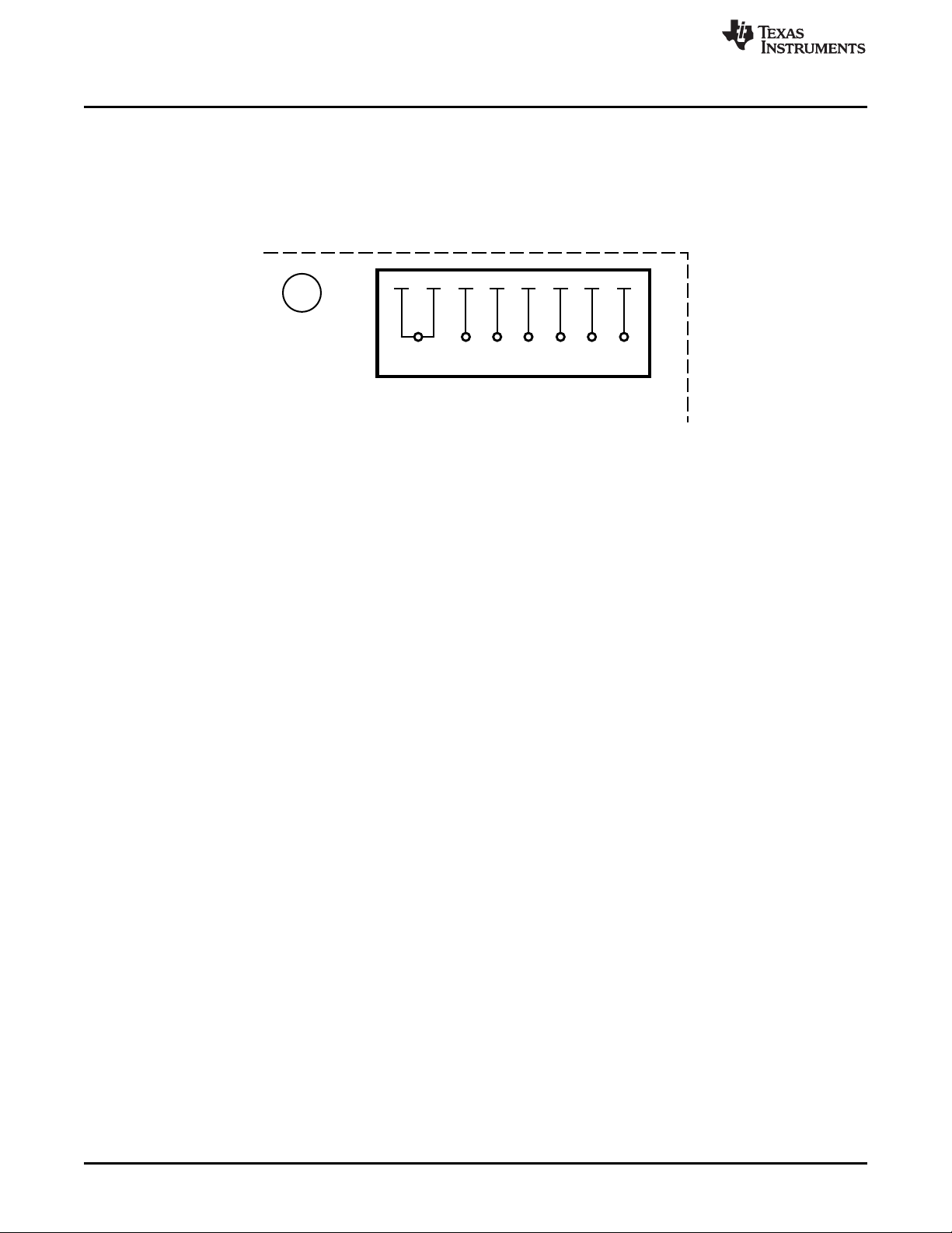
LEDs can be connected either via the 8-pin header or to the terminal posts. Figure 1 shows the pinout of
the header.
Connect the input voltage supply to the VIN and GND posts.
When all connections and polarities have been verified, power can be applied. When the input voltage
rises above 7.7V typically, the EN pin will cross the UVLO threshold and the LM3431 will startup. EN can
be pulled low (via the EN post) to shutdown the evaluation board.
www.ti.com
Figure 1. LED Connection, Top View Header Pinout
2
AN-1764 LM3431 Evaluation Board SNVA309A–January 2008–Revised May 2013
Copyright © 2008–2013, Texas Instruments Incorporated
Submit Documentation Feedback
Page 3
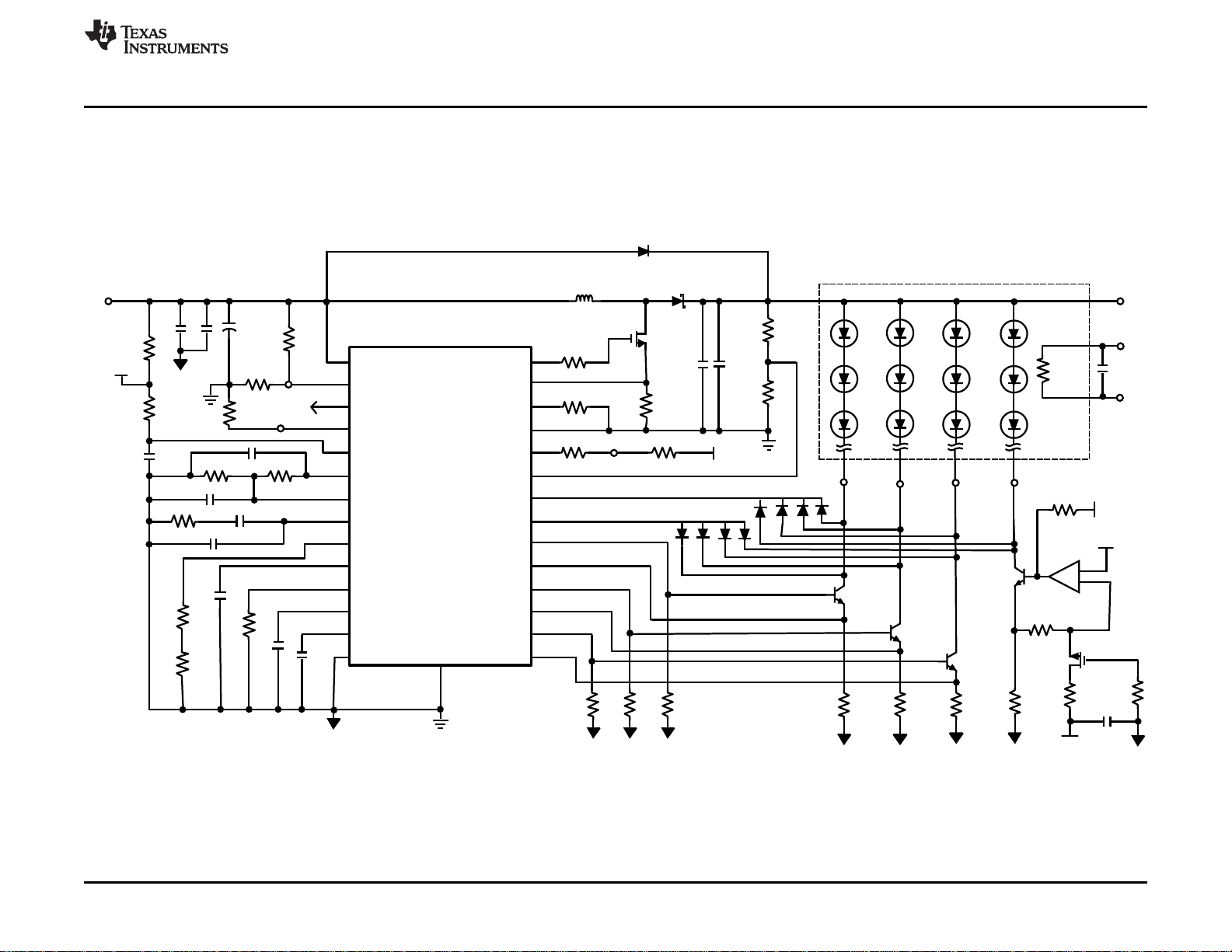
LM3431
VIN
EN
FF
SGND
AFB
VCC
REF
REFIN
SNS1
NDRV3
SNS3
NDRV1
NDRV2
SNS2
LG
CS
PGND
COMP
MODE/F
RT
CFB
THM
SC
SS/SH
DLY
DIM
ILIM
Vin: 8V to 18V
LEDOFF
+
-
REFIN
LEDOFF
VCC
D2-5 3003C
D6-9 1001A
D1 40V 2A
L1
7 PH 3.1A
Q1
Si4446
C10*
R19
562k
R18
33.2k
R3
51m:
R4 5.76k
C1
1 PF
C2
10 PF
R2
20k
R1
105k
R7 88.7k
R8 13k
R9 909:
C4 47 nF
R5b
15.8k
C3
4.7 PF
R6
34.8k
C6
47 nF
C7
4.7 nF
VCC
R10
2.2:
Q2
2N2222
Q6
2N7002k
LED ARRAY = 4 x 8 @140 mA
R15 1k
VA
VC1
VC2
VC3
VC4
RMODE
0:
C5
10 nF
THM
R17 95.3k
VCC
Op1
LMV710
THM
External
Thermistor
C11 *
EP
C8,C9
4.7 PF
Q3
2N2222
Q4
2N2222
Q5
2N2222
R11
2.2:
R12
2.2:
R14
10k
* = not installed
R16 10k
Rrestart
*
C13 *
+
10 nF
8V to 18V input
700 kHz switching, 180 Hz ± 1 kHz dimming
4 strings of 8 LEDs, 140 mA per string
R13
2.2:
VCC
R24 *
GND
C14
*
D10 *
C12 *
R5a
0:
R21 - R23
*
RVCC
*
C16*
DIM
R20 *
EN
R25 0:
C15
www.ti.com
Before Powering Up
SNVA309A–January 2008–Revised May 2013 AN-1764 LM3431 Evaluation Board
Figure 2. Complete LM3431 Eval Board Schematic
Submit Documentation Feedback
Copyright © 2008–2013, Texas Instruments Incorporated
3
Page 4

Bill of Materials
3 Bill of Materials
Ref # Function Description Part Number Manufacturer
IC1 Boost controller and LED driver LM3431 Texas Instruments
C1 Cin 1µF 50V B ceramic GRM32RB11H105KA01 Murata
C2 Cin 10µF 50V electrolytic UUD1H100MCL Nichicon
C3 VCC 4.7µF 10V X7R ceramic C2012X7R1A475M TDK
C4 Comp 47nF 50V X7R ceramic GRM21BR71H473KA01L3K Murata
C5 MODE/F 10nF 10V COG ceramic GRM2195C1H103JA01D Murata
C6 SS 47nF 50V X7R ceramic GRM21BR71H473KA01L3K Murata
C7 DLY 4.7nF 50V COG ceramic GRM2165C1H472JA01D Murata
C8 VA 4.7µF 50V X7R ceramic GRM32ER71H475KA88L Murata
C9 VA 4.7µF 50V X7R ceramic GRM32ER71H475KA88L Murata
C10 VA not installed - C11 REFIN bypass not installed - C12 REF bypass not installed - C13 Comp2 not installed - C14 THM not installed - C15 OP1 10nF 10V COG ceramic GRM2195C1H103JA01D Murata
C16 Cin not installed - -
D1 power diode 2A 40V Schottky diode SS24 Vishay
D2-D3 SC 600mA dual cathode diode CMPD3003C Central
D4-D5 SC 600mA dual cathode diode CMPD3003C Central
D6-D7 CFB 250mA dual anode diode CMPD1001A Central
D8-D9 CFB 250mA dual anode diode CMPD1001A Central
D10 bypass diode not installed - -
L1 power coil 7µH 3.1A inductor MSS1038-702NL Coilcraft
Op1 ch.4 rail to rail op amp LMV710 Texas Instruments
Q1 Power FET 4A 40V N-channel MOSFET Si4446DY Vishay
Q2-Q5 regulator 40V 600mA NPN transistor CXT2222A Central
Q6 ch.4 60V 200mA N-channel MOSFET 2N7002K Vishay
R1 EN uvlo set 105k 1%
R2 EN uvlo set 20k
R3 I sense 51mohm 0.5W 1% WSL2010R0510F Vishay
R4 I limit 5.76k 1%
R5a FF 0Ω
R5b FF 15.8k 1%
R6 RT 34.8k
R7 REFIN set 88.7k 1%
R8 REFIN set 13.0k 1%
R9 Comp 909Ω 1%
R10 - R13 LED sense 2.2Ω 1%
R14 ch.4 10k
R15 ch.4 1k
R16 DIM 10k
www.ti.com
Table 1. Standard Bill of Materials
Semiconductor
Semiconductor
Semiconductor
Semiconductor
Semiconductor
4
AN-1764 LM3431 Evaluation Board SNVA309A–January 2008–Revised May 2013
Copyright © 2008–2013, Texas Instruments Incorporated
Submit Documentation Feedback
Page 5

www.ti.com
Ref # Function Description Part Number Manufacturer
R17 THM 95.3k
R18 AFB 33.2k
R19 AFB 562k
R20 HG not installed - -
R21 - R23 NDRV not installed - -
R24 ch.4 not installed - R25 THM hys 0Ω
Rmode MODE/F 0Ω
Rrestart restart select not installed - -
RVCC not installed - -
4 Optional Components
Several of the components shown in the schematic are not installed and are optional. These components
are typically not required, but may be useful in some applications.C10 is provided for adding additional
output capacitance or for using more capacitors with smaller case sizes.C11 and C12 can be used to filter
reference voltage noise. Noise at the REF_IN pin can appear as noise in the LED current. Whether these
capacitors are required depends on the amount of switching noise, type of NPN used, and how much
noise is tolerable in the LED current. C13 is a second compensation capacitor, which may be required if a
high ESR output capacitor is used. Refer to the SNVS547 data sheet for details.
D10 provides a current path from VIN to VA during startup. By bypassing the inductor, D10 prevents VA
from rising above VIN at the initial power-on. In some conditions an OVP fault may occur at startup
without D10 installed.
R20 is a gate drive resistor for the NFET, Q1. An R20 value of up to 10Ω can be used to reduce the rise
and fall time of the gate drive to reduce switching noise. To install R20, first cut the trace between the R20
pads.
R21-R23 are NDRV pull-down resistors. A value of 300Ω to 1k can reduce LED current noise. These
resistors are typically most effective when driving NFET current regulators. RVCC connects VCC to VIN.
For 5V input applications, a 4.7Ω resistor should be installed here to pull-up VCC. For these applications,
additional input capacitance at C16 may also be required.
R-restart enables the automatic restart function. Auto-restart cannot be enabled when four LED channels
are used. If three or fewer channels are being driven, install R-restart with 0Ω to enable the auto-restart
function, which restarts the LM3431 after a fault shutdown.
R-MODE selects the DIM control mode as was described previously. For lower current applications, there
is a second Q1 pad which fits SOT-23 size NFETs.
An external NTC thermistor can be connected either between the THM pad and SGND terminal post or via
pins 7 and 8 on the 8-pin header. This thermistor is used to monitor LED temperature. With the installed
R17 value, the LM3431 will enter standby when the thermistor resistance falls to 31kΩ. For example, a
thermistor with a 25°C resistance of 680k and a beta constant of 4125 will yield a shutdown temperature
of 110°C.
R25 is a hysteresis resistor for the THM function. The default value is 0Ω which results in a restart
hysteresis of 10°C. Use R25 to increase the THM hysteresis according to the data sheet description.
C14 can be installed as a noise filter for the external thermistor voltage.
Optional Components
Table 1. Standard Bill of Materials (continued)
SNVA309A–January 2008–Revised May 2013 AN-1764 LM3431 Evaluation Board
Submit Documentation Feedback
Copyright © 2008–2013, Texas Instruments Incorporated
5
Page 6

LED String Options
5 LED String Options
Table 2 and Table 3 give the required component changes for driving LED arrays other than the default.
The values shown assume a typical LED Vf of 3.2V at 140mA. These tables are designed for simplicity
and ease of modification, not optimum performance. Therefore, any of the changes listed below will result
in a lower maximum contrast ratio as compared to the default LED array. For optimum performance, all
component values should be reviewed. R5 in the tables refers to the sum of R5a and R5b shown on the
schematic. For the best performance, R5 can be manually adjusted for the specific input voltage, dimming
frequency, and LED current of each application.
LED current R7 R8 R5
160mA 78.7k 13k nc
130mA 100k 13k 17.4k
115mA 115k 13k 18.7k
100mA 93.1k 9.09k 20k
2 Strings
# of LEDs R19 R3 R5 R6
6 432k 80m 24.9k 43.2k
7 499k 90m 28.7k 26.7k
8 nc 70m 30.1k 23.2k
3 Strings
6 432k nc 28k 43.2k
7 499k nc 24.3k nc
8 nc nc 20k nc
9 634k nc 19.1k 30.1k
4 Strings
6 432k nc 19.1k 43.2k
7 499k nc 16.9k nc
9 634k 40m 14.3k nc
www.ti.com
Table 2. LED Current Settings (nc = no change)
Table 3. LED Array Options at 140mA Setting
(nc = no change)
6
AN-1764 LM3431 Evaluation Board SNVA309A–January 2008–Revised May 2013
Copyright © 2008–2013, Texas Instruments Incorporated
Submit Documentation Feedback
Page 7

50
60
70
80
90
100
8 10 12 14 16 18
EFFICIENCY (%)
INPUT VOLTAGE (V)
400 Ps/DIV
VC1
2V/Div
DLY
1V/Div
Iout
500 mA/Div
0
100:1
200:1
300:1
400:1
500:1
600:1
700:1
0 200 400 600 800 1000 1200
DIMMING FREQUENCY (Hz)
MAX CONTRAST RATIO
1 ms/DIV
VA
10V/Div
VIN
10V/Div
SS/SH
1V/Div
ILED
50 mA/Div
www.ti.com
6 Typical Evaluation Board Performance
Unless otherwise specified, the following conditions apply: Vin = 12V, Ta = 25°C, LED array = 4 parallel
strings of 8 LEDs at 140mA per string. LED part number: Nichia NFSW036BT.
Typical Evaluation Board Performance
Figure 3. Maximum Contrast Ratio vs. Dimming Figure 4. Power-On Startup Waveforms
Frequency
Figure 5. Fault Delay Waveforms Figure 6. Efficiency vs. Input Voltage
(one LED open)
SNVA309A–January 2008–Revised May 2013 AN-1764 LM3431 Evaluation Board
Submit Documentation Feedback
7
Copyright © 2008–2013, Texas Instruments Incorporated
Page 8

1 Ps/DIV
VA
500 mV/Div
ILED
5 mA/Div
VC1
1V/Div
SW
10V/Div
4 Ps/DIV
VC1
2V/Div
VA
500 mV/Div
ILED
50 mA/Div
Typical Evaluation Board Performance
Figure 7. Typical Dimming Waveforms Figure 8. Boost Switching Waveforms
(1kHz at 1% duty)
www.ti.com
8
AN-1764 LM3431 Evaluation Board SNVA309A–January 2008–Revised May 2013
Copyright © 2008–2013, Texas Instruments Incorporated
Submit Documentation Feedback
Page 9

www.ti.com
7 PCB Layout
PCB Layout
Figure 9. Top Side PCB Layout
Figure 10. Bottom Side PCB Layout
SNVA309A–January 2008–Revised May 2013 AN-1764 LM3431 Evaluation Board
Submit Documentation Feedback
Copyright © 2008–2013, Texas Instruments Incorporated
9
Page 10

IMPORTANT NOTICE
Texas Instruments Incorporated and its subsidiaries (TI) reserve the right to make corrections, enhancements, improvements and other
changes to its semiconductor products and services per JESD46, latest issue, and to discontinue any product or service per JESD48, latest
issue. Buyers should obtain the latest relevant information before placing orders and should verify that such information is current and
complete. All semiconductor products (also referred to herein as “components”) are sold subject to TI’s terms and conditions of sale
supplied at the time of order acknowledgment.
TI warrants performance of its components to the specifications applicable at the time of sale, in accordance with the warranty in TI’s terms
and conditions of sale of semiconductor products. Testing and other quality control techniques are used to the extent TI deems necessary
to support this warranty. Except where mandated by applicable law, testing of all parameters of each component is not necessarily
performed.
TI assumes no liability for applications assistance or the design of Buyers’ products. Buyers are responsible for their products and
applications using TI components. To minimize the risks associated with Buyers’ products and applications, Buyers should provide
adequate design and operating safeguards.
TI does not warrant or represent that any license, either express or implied, is granted under any patent right, copyright, mask work right, or
other intellectual property right relating to any combination, machine, or process in which TI components or services are used. Information
published by TI regarding third-party products or services does not constitute a license to use such products or services or a warranty or
endorsement thereof. Use of such information may require a license from a third party under the patents or other intellectual property of the
third party, or a license from TI under the patents or other intellectual property of TI.
Reproduction of significant portions of TI information in TI data books or data sheets is permissible only if reproduction is without alteration
and is accompanied by all associated warranties, conditions, limitations, and notices. TI is not responsible or liable for such altered
documentation. Information of third parties may be subject to additional restrictions.
Resale of TI components or services with statements different from or beyond the parameters stated by TI for that component or service
voids all express and any implied warranties for the associated TI component or service and is an unfair and deceptive business practice.
TI is not responsible or liable for any such statements.
Buyer acknowledges and agrees that it is solely responsible for compliance with all legal, regulatory and safety-related requirements
concerning its products, and any use of TI components in its applications, notwithstanding any applications-related information or support
that may be provided by TI. Buyer represents and agrees that it has all the necessary expertise to create and implement safeguards which
anticipate dangerous consequences of failures, monitor failures and their consequences, lessen the likelihood of failures that might cause
harm and take appropriate remedial actions. Buyer will fully indemnify TI and its representatives against any damages arising out of the use
of any TI components in safety-critical applications.
In some cases, TI components may be promoted specifically to facilitate safety-related applications. With such components, TI’s goal is to
help enable customers to design and create their own end-product solutions that meet applicable functional safety standards and
requirements. Nonetheless, such components are subject to these terms.
No TI components are authorized for use in FDA Class III (or similar life-critical medical equipment) unless authorized officers of the parties
have executed a special agreement specifically governing such use.
Only those TI components which TI has specifically designated as military grade or “enhanced plastic” are designed and intended for use in
military/aerospace applications or environments. Buyer acknowledges and agrees that any military or aerospace use of TI components
which have not been so designated is solely at the Buyer's risk, and that Buyer is solely responsible for compliance with all legal and
regulatory requirements in connection with such use.
TI has specifically designated certain components as meeting ISO/TS16949 requirements, mainly for automotive use. In any case of use of
non-designated products, TI will not be responsible for any failure to meet ISO/TS16949.
Products Applications
Audio www.ti.com/audio Automotive and Transportation www.ti.com/automotive
Amplifiers amplifier.ti.com Communications and Telecom www.ti.com/communications
Data Converters dataconverter.ti.com Computers and Peripherals www.ti.com/computers
DLP® Products www.dlp.com Consumer Electronics www.ti.com/consumer-apps
DSP dsp.ti.com Energy and Lighting www.ti.com/energy
Clocks and Timers www.ti.com/clocks Industrial www.ti.com/industrial
Interface interface.ti.com Medical www.ti.com/medical
Logic logic.ti.com Security www.ti.com/security
Power Mgmt power.ti.com Space, Avionics and Defense www.ti.com/space-avionics-defense
Microcontrollers microcontroller.ti.com Video and Imaging www.ti.com/video
RFID www.ti-rfid.com
OMAP Applications Processors www.ti.com/omap TI E2E Community e2e.ti.com
Wireless Connectivity www.ti.com/wirelessconnectivity
Mailing Address: Texas Instruments, Post Office Box 655303, Dallas, Texas 75265
Copyright © 2013, Texas Instruments Incorporated
 Loading...