

Page 1
C535676
Connector
P6
P1
Anode of
First LED
Cathode of
Last LED
User's Guide
SNVA175C–September 2006–Revised April 2013
AN-1500 LM3402/02HV Demo Board
1 Introduction
The LM3402/LM3402HV is a buck regulator derived controlled current source designed to drive a series
string of high power, high brightness LEDs (HBLEDs) such as the Luxeon™ I Emitter at forward currents
of up to 500 mA. The board can accept an input voltage ranging from 6V to 42V when using the LM3402.
When using the pin-for-pin compatible LM3402HV the upper bound of input voltage is 75V. The converter
output voltage adjusts as needed to maintain a constant current through the LED array. The
LM3402/02HV is a true step-down regulator with an output voltage range extending from a V
mV (the reference voltage) to a V
maintain regulated current through any number of LEDs as long as the combined forward voltage of the
array does not exceed V
O(MAX).
.
2 Circuit Performance LM3402
The LM3402 circuit and BOM have been designed to provide a constant forward current of 350 mA to a
single LED with a forward voltage of approximately 3.5V. (Typical of white, blue, and green LEDs using
InGaN technology.) When powered from a 24V ±5% input the demo board will maintain the average LED
current, IF, to within 10% of 350 mA. The ripple current, ΔiF, will not exceed 70 mA peak-to-peak.
Switching frequency for the demo board is 600 kHz ± 10% over the input voltage range of 6V to 42V.
determined by the minimum off time (typically 300 ns). It can
O(MAX)
O(MIN)
of 200
3 Circuit Performance LM3402HV
The LM3402HV circuit and BOM have been designed to provide a constant forward current of 350 mA to
a single LED with a forward voltage of approximately 3.5V. When powered from a 48V ± 5% input the
demo board will maintain IFto within ±5% of 350 mA. Ripple current will not exceed 70 mA peak-to-peak.
Switching frequency for the demo board is 250 kHz ±10% over the input voltage range of 6V to 75V.
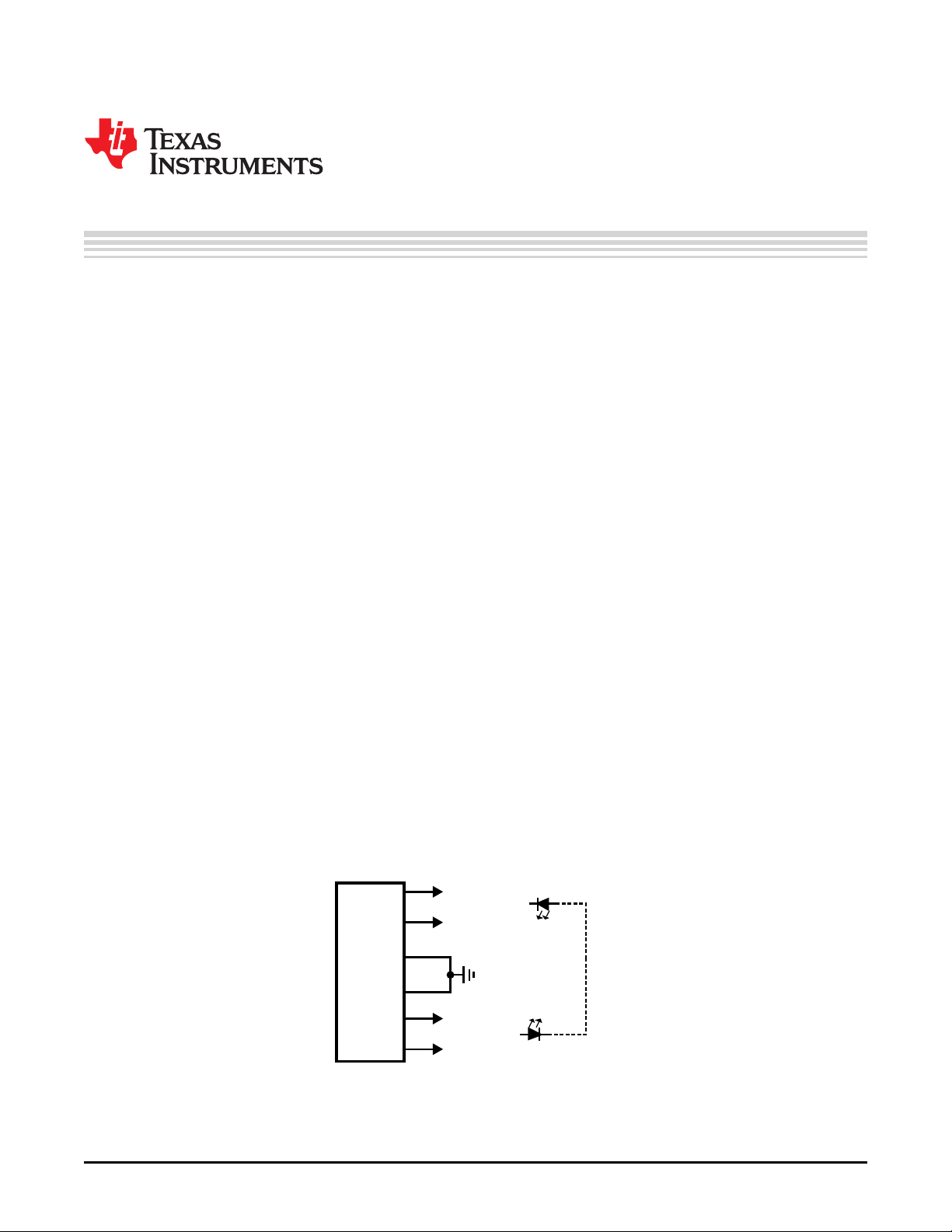
4 Connecting to LED Array
The LM3402/02HV demo board includes a female 6-pin SIP, J1, connector as well as two standard 94mil
turret connectors for the cathode and anode connections of the LED array. Figure 1 shows the pinout of
J1. Solid, 18 or 20 gauge wire with about 1 cm of insulation stripped away makes a convenient, solderless
connection to J1.
Figure 1. Connecting to LED Array
All trademarks are the property of their respective owners.
SNVA175C–September 2006–Revised April 2013 AN-1500 LM3402/02HV Demo Board
Submit Documentation Feedback
Copyright © 2006–2013, Texas Instruments Incorporated
1
Page 2
T
D
t
D
t
SD
tDtSUt
SD
tDt
SU
t
SD
D
MIN
D
MAX
T T
DIM
I
F
f
PWM
T =
1
T
tD + t
SU
D
MIN
=
T
T + t
SD
D
MAX
=
t
SU
R
SNS
=
2
VIN - V
O
0.2 x L
IF x L + VO x t
SNS
-
x t
ON
Setting the LED Current
5 Setting the LED Current
www.ti.com
The default forward current I
this value the current setting resistor R
t
= 220 ns (2)
SNS
delivered to the LED array is 350 mA, typical of many 1W LEDs. To adjust
LED
can be changed according to the following equation:
SNS
This resistor should be rated to handle the power dissipation of the LED current. For example, the closest
5% tolerance resistor to set an LED current of 350 mA is 0.56 Ω. In steady state this resistor will dissipate
(0.352 × 0.56) = 69 mW, indicating that a resistor with a 1/8W power rating is appropriate.
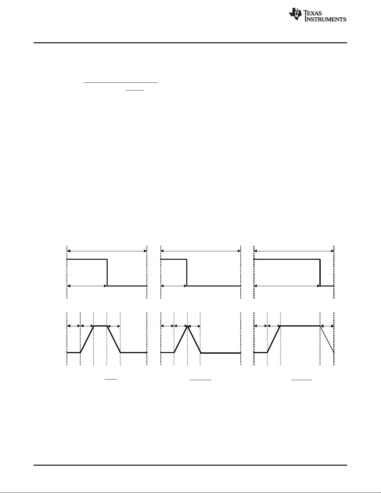
6 PWM Dimming
The DIM1 terminal on the PCB provides an input for a pulse width modulation signal for dimming of the
LED array. In order to fully enable and disable the LM3402/02HV the PWM signal should have a
maximum logic low level of 0.8V and a minimum logic high level of 2.2V. The maximum PWM dimming
frequency, minimum PWM duty cycle and maximum duty cycle are illustrated in Figure 2. PWM frequency
should be at least one order of magnitude below the LM3402/02HV switching frequency. The interval t
represents the delay from a logic high at the DIM pin to the onset of the output current. The quantities t
and tSDrepresent the time needed for the output current to slew up to steady state and slew down to zero,
respectively. Typical response times for the standard LM3402 and LM3402HV demo boards circuits are
shown in Section 11.
(1)
D
SU
Figure 2. PWM Dimming Limits
The logic of DIM1 is direct, hence the LM3402/02HV will deliver regulated output current when the voltage
at DIM1 is high, and the current output is disabled when the voltage at DIM1 is low. Connecting a constant
logic low will disable the output, and the LM3402/02HV is enabled if the DIM pin is open-circuited. The
DIM1 function disables only the power NFET, leaving all other circuit blocks functioning to minimize the
converter response time.
2
AN-1500 LM3402/02HV Demo Board SNVA175C–September 2006–Revised April 2013
Copyright © 2006–2013, Texas Instruments Incorporated
Submit Documentation Feedback
Page 3
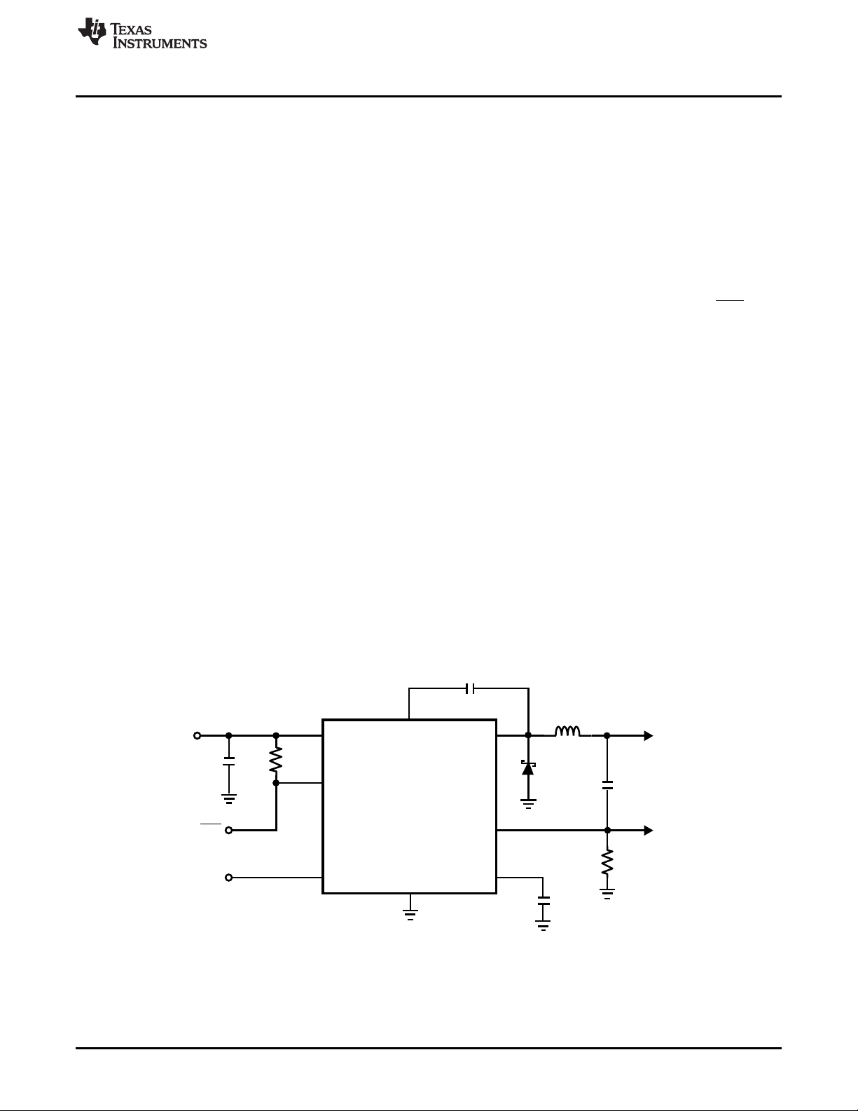
GND
DIM
BOOT
SW
CS
RON
LM3402/02HV
VIN
D1
L1
C
B
R
SNS
C
F
R
ON
C
IN
VIN = 6V to 42V (LM3402)
VIN = 6V to 75V (LM3402HV)
VCC
C
O1
OFF
DIM1
LED
ANODE
LED
CATHODE
1
2
3
4
5
6
7
8
(used in BOM 2 only)
www.ti.com
Low Power Shutdown
The DIM2 terminal provides a second method for PWM dimming by connecting to the gate of an optional
NFET, Q1. Note that Q1 is not provided on the standard BOM, and must be added for the DIM2 function
to operate. Q1 provides a parallel path for the LED current. This small NFET can be turned on and off
much more quickly than the LM3402/02HV can shutdown the internal NFET, providing faster response
time for higher frequency and/or greater resolution in the PWM dimming signal. The tradeoff in this
method is that the full current flows through Q1 while the LED is off, resulting in lower efficiency.
The logic of DIM2 is inverted, hence the LM3402/02HV will deliver regulated output current when the
voltage at DIM2 is low, and the current output is disabled when the voltage at DIM2 is high. Connecting a
constant logic high to the DIM2 will turn off the LED but will not shut down the LM3402/02HV.
7 Low Power Shutdown
The LM3402/02HV can be placed into a low power shutdown (typically 90 µA) by grounding the OFF
terminal. During normal operation this terminal should be left open-circuit.
8 Output Open Circuit
With either DIM terminal floating or connected to logic high, the LM3402/02HV will begin to operate as
soon as it has an input of at least 6V. In the case that the input is powered but no LED array is connected
the output voltage will rise to equal the input voltage. The output of the circuit is rated to 50V (LM3402) or
100V (LM3402HV) and will not suffer damage, however care should be taken not to connect an LED array
if the output voltage is higher than the target forward voltage of the LED array in steady state.
Alternatively, a zener diode and zener current limiting resistor can be placed in the positions Z1 and RZ. In
the case of an accidental open circuit at the output Z1 will enter reverse bias and attempt to pull the CS
pin voltage up to the output voltage. An internal comparator monitors the CS pin voltage and will disable
the internal NFET in this case. The result is a low power hiccup mode, designed to prevent excessive
voltage at the output and thermal stress on the inductor, internal NFET, and input voltage source.
Figure 3. Standard Schematic
SNVA175C–September 2006–Revised April 2013 AN-1500 LM3402/02HV Demo Board
Submit Documentation Feedback
Copyright © 2006–2013, Texas Instruments Incorporated
3
Page 4
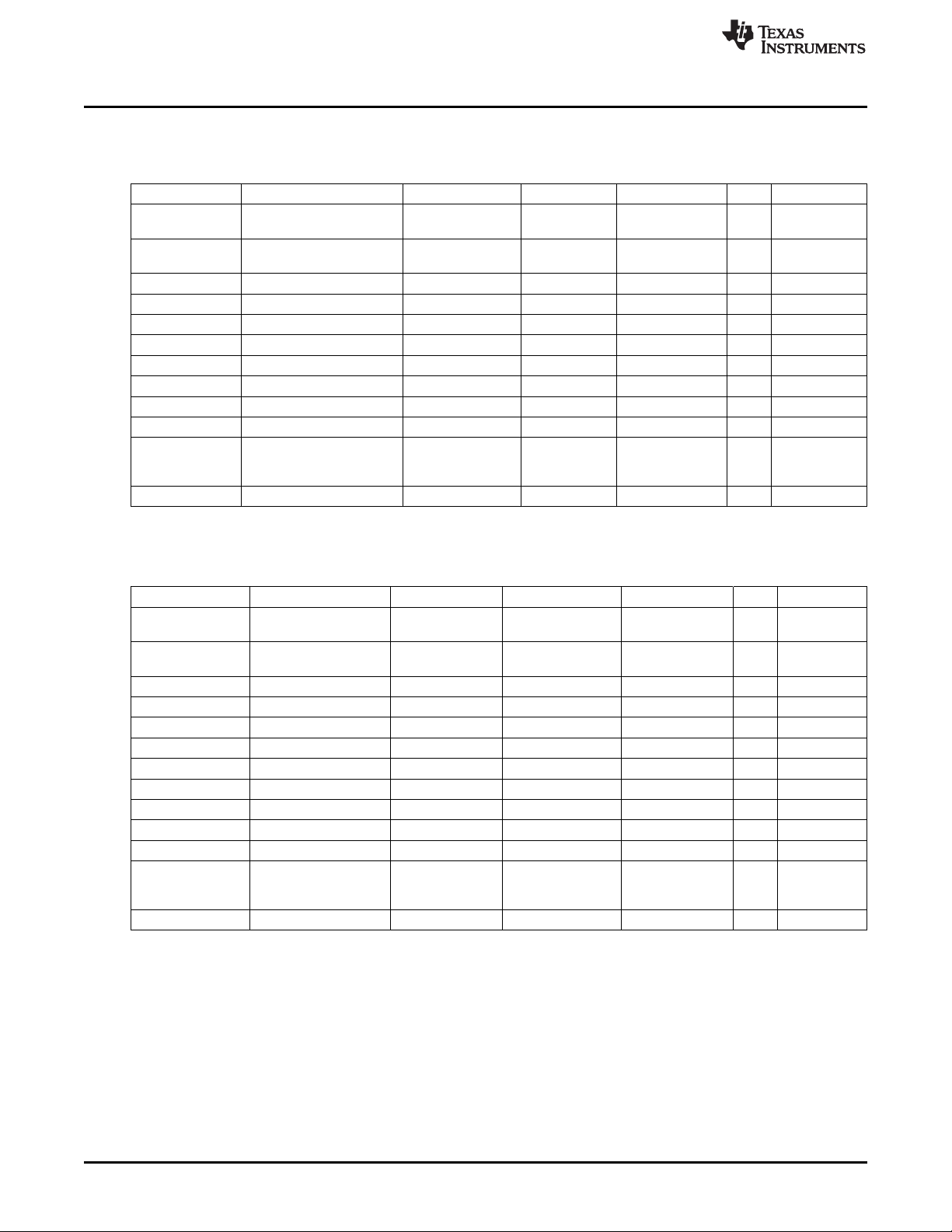
Bill of Materials
9 Bill of Materials
ID Part Number Type Size Parameters Qty Vendor
U1 LM3402 LED Driver VSSOP-8 42V, 0.5A 1 Texas
L1 SLF10145T-101M1R0 Inductor 10.1 × 10.1 × 100µH, 1A, 0.2Ω 1 TDK
D1 CMSH1-60M Schottky Diode SMA 60V, 1A 1 Central Semi
Cf VJ0805Y104KXXAT Capacitor 0805 100nF 10% 1 Vishay
Cb VJ0805Y103KXXAT Capacitor 0805 10nF 10% 1 Vishay
Cin C3216X7R1H105M Capacitor 1206 1µF 50V 1 TDK
Rsns ERJ6BQFR56V Resistor 0805 0.56Ω 1% 1 Panasonic
Ron CRCW08054642F Resistor 0805 46.4kΩ 1% 1 Vishay
Rz CRCW08050R00F Resistor 0805 0Ω 1 Vishay
DIM1, DIM2 160-1512 Terminal Silver 0.062” 2 Cambion
GND1, GND2, 160-1026 Terminal Silver 0.094” 7 Cambion
GND3, VIN, ISNS
/ C, Vo / A, SW
J1 535676-5 Connector Custom 6 Pins 1 Tyco/AMP
www.ti.com
Table 1. Bill of Materials (LM3402)
Instruments
4.5mm
Table 2. Bill of Materials (LM3402HV)
ID Part Number Type Size Parameters Qty Vendor
U1 LM3402HV LED Driver VSSOP-8 75V, 0.5A 1 Texas
L1 SLF10145T-151MR79 Inductor 10.1 × 10.1 × 150µH, 0.8A, 1 TDK
4.5mm 0.2Ω
D1 CMSH1-100M Schottky Diode SMA 100V, 1A 1 Central Semi
Cf VJ0805Y104KXXAT Capacitor 0805 100nF 10% 1 Vishay
Cb VJ0805Y103KXXAT Capacitor 0805 10nF 10% 1 Vishay
Cin C3225X7R2A105M Capacitor 1210 1µF 100V 1 TDK
Co1 C3216X7R1E225M Capacitor 1206 2.2µF 25V 1 TDK
Rsns ERJ6BQFR68V Resistor 0805 0.68Ω 1% 1 Panasonic
Ron CRCW08051303F Resistor 0805 130kΩ 1% 1 Vishay
Rz CRCW08050R00F Resistor 0805 0Ω 1 Vishay
DIM1, DIM2 160-1512 Terminal Silver 0.062” 2 Cambion
GND1, GND2, 160-1026 Terminal Silver 0.094” 7 Cambion
GND3, VIN, ISNS /
C, Vo / A, SW
J1 535676-5 Connector Custom 6 Pins 1 Tyco/AMP
Instruments
4
AN-1500 LM3402/02HV Demo Board SNVA175C–September 2006–Revised April 2013
Copyright © 2006–2013, Texas Instruments Incorporated
Submit Documentation Feedback
Page 5

GND
DIM
BOOT SW
CS
RON
LM3402/02HV
VIN
D1
L1
C
B
R
SNS
C
F
R
ON
C
IN
VIN = 6V to 42V (LM3402)
VIN = 6V to 75V (LM3402HV)
VCC
C
O1
OFF
DIM1
LED
ANODE
LED
CATHODE
R
Z
C
O2
R
ESR
R
PD
DIM2
R
SNB
C
SNB
Z1
Q1
7
5
1
2
4
3
6
8
www.ti.com
10 Evaluation Board Schematic
Figure 4. Complete Evaluation Board Schematic
Evaluation Board Schematic
SNVA175C–September 2006–Revised April 2013 AN-1500 LM3402/02HV Demo Board
Submit Documentation Feedback
Copyright © 2006–2013, Texas Instruments Incorporated
5
Page 6

Typical Performance Characteristics
11 Typical Performance Characteristics
Efficiency for Table 1 Efficiency for Table 2
TA= 25°C, IF= 350 mA TA= 25°C, IF= 350 mA
IFvs VINfor Table 1 IFvs VINfor Table 2
TA= 25°C TA= 25°C
www.ti.com
6
AN-1500 LM3402/02HV Demo Board SNVA175C–September 2006–Revised April 2013
Copyright © 2006–2013, Texas Instruments Incorporated
Submit Documentation Feedback
Page 7

10 és/DIV
5V/DIV
100 mA/DIV
I
F
DIM
4 és/DIV
5V/DIV
100 mA/DIV
I
F
DIM
1 és/DIV
10V/DIV
100 mA/DIV
SW
I
F
1 és/DIV
10 mA/DIV
I
F
1 és/DIV
5V/DIV
100 mA/DIV
I
F
DIM
2 és/DIV
5V/DIV
100 mA/DIV
I
F
DIM
www.ti.com
Typical Performance Characteristics
DIM Pin Enable Table 1 DIM Pin Disable Table 1
Switching Waveforms for Table 1 Output Ripple Current Table 1
DIM Pin Enable Table 2 DIM Pin Disable Table 2
SNVA175C–September 2006–Revised April 2013 AN-1500 LM3402/02HV Demo Board
Submit Documentation Feedback
Copyright © 2006–2013, Texas Instruments Incorporated
7
Page 8

2 és/DIV
20V/DIV
100 mA/DIV
SW
I
F
2 és/DIV
5 mA/DIV
I
F
Typical Performance Characteristics
Switching Waveforms for Table 2 Output Ripple Current Table 2
www.ti.com
8
AN-1500 LM3402/02HV Demo Board SNVA175C–September 2006–Revised April 2013
Copyright © 2006–2013, Texas Instruments Incorporated
Submit Documentation Feedback
Page 9

www.ti.com
12 Layout
Layout
Figure 5. Top Layer and Top Overlay
SNVA175C–September 2006–Revised April 2013 AN-1500 LM3402/02HV Demo Board
Submit Documentation Feedback
Copyright © 2006–2013, Texas Instruments Incorporated
9
Page 10

Layout
www.ti.com
Figure 6. Bottom Layer and Bottom Overlay
10
AN-1500 LM3402/02HV Demo Board SNVA175C–September 2006–Revised April 2013
Copyright © 2006–2013, Texas Instruments Incorporated
Submit Documentation Feedback
Page 11

IMPORTANT NOTICE
Texas Instruments Incorporated and its subsidiaries (TI) reserve the right to make corrections, enhancements, improvements and other
changes to its semiconductor products and services per JESD46, latest issue, and to discontinue any product or service per JESD48, latest
issue. Buyers should obtain the latest relevant information before placing orders and should verify that such information is current and
complete. All semiconductor products (also referred to herein as “components”) are sold subject to TI’s terms and conditions of sale
supplied at the time of order acknowledgment.
TI warrants performance of its components to the specifications applicable at the time of sale, in accordance with the warranty in TI’s terms
and conditions of sale of semiconductor products. Testing and other quality control techniques are used to the extent TI deems necessary
to support this warranty. Except where mandated by applicable law, testing of all parameters of each component is not necessarily
performed.
TI assumes no liability for applications assistance or the design of Buyers’ products. Buyers are responsible for their products and
applications using TI components. To minimize the risks associated with Buyers’ products and applications, Buyers should provide
adequate design and operating safeguards.
TI does not warrant or represent that any license, either express or implied, is granted under any patent right, copyright, mask work right, or
other intellectual property right relating to any combination, machine, or process in which TI components or services are used. Information
published by TI regarding third-party products or services does not constitute a license to use such products or services or a warranty or
endorsement thereof. Use of such information may require a license from a third party under the patents or other intellectual property of the
third party, or a license from TI under the patents or other intellectual property of TI.
Reproduction of significant portions of TI information in TI data books or data sheets is permissible only if reproduction is without alteration
and is accompanied by all associated warranties, conditions, limitations, and notices. TI is not responsible or liable for such altered
documentation. Information of third parties may be subject to additional restrictions.
Resale of TI components or services with statements different from or beyond the parameters stated by TI for that component or service
voids all express and any implied warranties for the associated TI component or service and is an unfair and deceptive business practice.
TI is not responsible or liable for any such statements.
Buyer acknowledges and agrees that it is solely responsible for compliance with all legal, regulatory and safety-related requirements
concerning its products, and any use of TI components in its applications, notwithstanding any applications-related information or support
that may be provided by TI. Buyer represents and agrees that it has all the necessary expertise to create and implement safeguards which
anticipate dangerous consequences of failures, monitor failures and their consequences, lessen the likelihood of failures that might cause
harm and take appropriate remedial actions. Buyer will fully indemnify TI and its representatives against any damages arising out of the use
of any TI components in safety-critical applications.
In some cases, TI components may be promoted specifically to facilitate safety-related applications. With such components, TI’s goal is to
help enable customers to design and create their own end-product solutions that meet applicable functional safety standards and
requirements. Nonetheless, such components are subject to these terms.
No TI components are authorized for use in FDA Class III (or similar life-critical medical equipment) unless authorized officers of the parties
have executed a special agreement specifically governing such use.
Only those TI components which TI has specifically designated as military grade or “enhanced plastic” are designed and intended for use in
military/aerospace applications or environments. Buyer acknowledges and agrees that any military or aerospace use of TI components
which have not been so designated is solely at the Buyer's risk, and that Buyer is solely responsible for compliance with all legal and
regulatory requirements in connection with such use.
TI has specifically designated certain components as meeting ISO/TS16949 requirements, mainly for automotive use. In any case of use of
non-designated products, TI will not be responsible for any failure to meet ISO/TS16949.
Products Applications
Audio www.ti.com/audio Automotive and Transportation www.ti.com/automotive
Amplifiers amplifier.ti.com Communications and Telecom www.ti.com/communications
Data Converters dataconverter.ti.com Computers and Peripherals www.ti.com/computers
DLP® Products www.dlp.com Consumer Electronics www.ti.com/consumer-apps
DSP dsp.ti.com Energy and Lighting www.ti.com/energy
Clocks and Timers www.ti.com/clocks Industrial www.ti.com/industrial
Interface interface.ti.com Medical www.ti.com/medical
Logic logic.ti.com Security www.ti.com/security
Power Mgmt power.ti.com Space, Avionics and Defense www.ti.com/space-avionics-defense
Microcontrollers microcontroller.ti.com Video and Imaging www.ti.com/video
RFID www.ti-rfid.com
OMAP Applications Processors www.ti.com/omap TI E2E Community e2e.ti.com
Wireless Connectivity www.ti.com/wirelessconnectivity
Mailing Address: Texas Instruments, Post Office Box 655303, Dallas, Texas 75265
Copyright © 2013, Texas Instruments Incorporated
 Loading...