

Page 1

User's Guide
SWRU382–November 2014
WL1837MODCOM8I WLAN MIMO and Bluetooth®Module
Evaluation Board for TI Sitara™ Platform
The WL1837MODCOM8I is a Wi-Fi®dual-band, Bluetooth, and BLE module evaluation board (EVB) with
the TI WL1837 module (WL1837MOD). The WL1837MOD is a certified WiLink™ 8 module from TI that
offers high throughput and extended range along with Wi-Fi and Bluetooth coexistence in a poweroptimized design. The WL1837MOD offers A 2.4- and 5-GHz module solution with two antennas
supporting industrial temperature grade. The module is FCC, IC, ETSI/CE, and TELEC certified for AP
(with DFS support) and client. TI offers drivers for high-level operating systems, such as Linux®,
Android™, WinCE, and RTOS.TI.
Contents
1 Overview...................................................................................................................... 3
1.1 General Features ................................................................................................... 3
1.2 Key Benefits......................................................................................................... 3
1.3 Applications.......................................................................................................... 4
2 Board Pin Assignment ...................................................................................................... 4
2.1 Pin Description ...................................................................................................... 5
2.2 Jumper Connections ............................................................................................... 7
3 Electrical Characteristics.................................................................................................... 7
4 Antenna Characteristics..................................................................................................... 8
4.1 VSWR ................................................................................................................ 8
4.2 Efficiency............................................................................................................. 8
4.3 Radio Pattern........................................................................................................ 9
5 Circuit Design ................................................................................................................ 9
5.1 EVB Reference Schematics....................................................................................... 9
5.2 Bill of Materials (BOM)............................................................................................ 10
6 Layout Guidelines .......................................................................................................... 11
6.1 Board Layout....................................................................................................... 11
7 Ordering Information....................................................................................................... 16
1 WL1837MODCOM8I EVB (Top View) .................................................................................... 3
2 EVB Top View................................................................................................................ 4
3 EVB (Bottom View).......................................................................................................... 5
4 Antenna VSWR Characteristics............................................................................................ 8
5 Antenna Efficiency........................................................................................................... 8
6 EVB Reference Schematics................................................................................................ 9
7 WL1837MODCOM8I Layer 1 Layout .................................................................................... 11
8 WL1837MODCOM8I Layer 2 Layout .................................................................................... 11
9 WL1837MODCOM8I Layer 3 Layout .................................................................................... 12
10 WL1837MODCOM8I Layer 4 Layout .................................................................................... 12
11 Module Layout Guidelines (Top Layer).................................................................................. 13
Sitara, WiLink are trademarks of Texas Instruments.
Bluetooth is a registered trademark of Bluetooth SIG, Inc.
Android is a trademark of Google, Inc.
Linux is a registered trademark of Linus Torvalds.
Wi-Fi is a registered trademark of Wi-Fi Alliance.
SWRU382–November 2014 WL1837MODCOM8I WLAN MIMO and Bluetooth®Module Evaluation Board
Submit Documentation Feedback
List of Figures
Copyright © 2014, Texas Instruments Incorporated
for TI Sitara™ Platform
1
Page 2

www.ti.com
12 Module Layout Guidelines (Bottom Layer).............................................................................. 13
13 Trace Design for the PCB Layout........................................................................................ 14
14 Layer 1 Combined With Layer 2.......................................................................................... 14
15 Top Layer – Antenna and RF Trace Routing Layout Guidelines .................................................... 15
16 Bottom Layer – Antenna and RF Trace Routing Layout Guidelines................................................. 15
17 MIMO Antenna Spacing................................................................................................... 16
List of Tables
1 Pin Description............................................................................................................... 5
2 BOM.......................................................................................................................... 10
3 Module Layout Guidelines ................................................................................................ 13
4 Antenna and RF Trace Routing Layout Guidelines.................................................................... 15
2
WL1837MODCOM8I WLAN MIMO and Bluetooth®Module Evaluation Board SWRU382–November 2014
for TI Sitara™ Platform
Copyright © 2014, Texas Instruments Incorporated
Submit Documentation Feedback
Page 3
www.ti.com
1 Overview
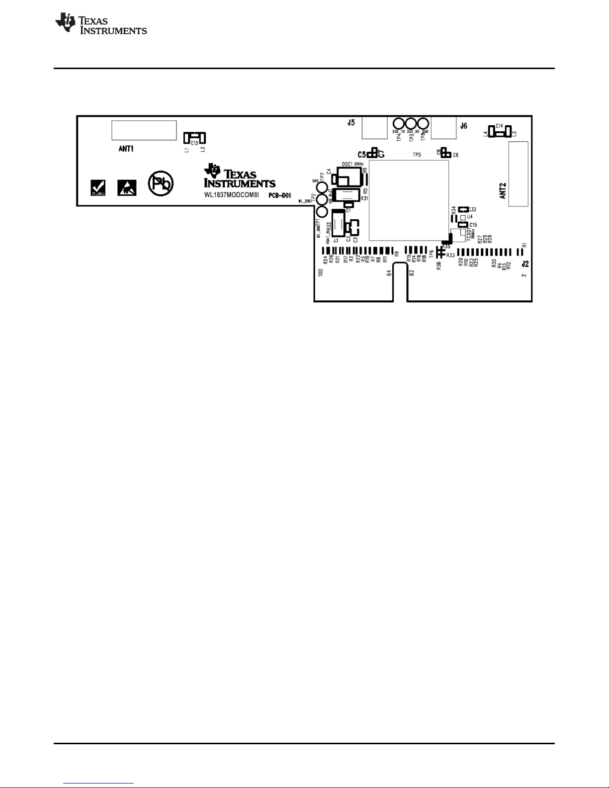
Figure 1 shows the WL1837MODCOM8I EVB.
Overview
Figure 1. WL1837MODCOM8I EVB (Top View)
1.1 General Features
The WL1837MODCOM8I EVB includes the following features:
• WLAN, Bluetooth, and BLE on a single module board
• 100-pin board card
• Dimensions: 76.0 mm (L) x 31.0 mm (W)
• WLAN 2.4- and 5-GHz SISO (20- and 40-MHz channels), 2.4-GHz MIMO (20-MHz channels)
• Support for BLE dual mode
• Seamless integration with TI Sitara and other application processors
• Design for the TI AM335X general-purpose evaluation module (EVM)
• WLAN and Bluetooth, BLE, and ANT cores that are software- and hardware-compatible with prior
WL127x, WL128x, and BL6450 offerings for smooth migration to device
• Shared host-controller-interface (HCI) transport for Bluetooth, BLE, and ANT using UART and SDIO for
WLAN
• Wi-Fi and Bluetooth single-antenna coexistence
• Built-in chip antenna
• Optional U.FL RF connector for external antenna
• Direct connection to the battery using an external switched-mode power supply (SMPS) supporting
2.9- to 4.8-V operation
• VIOin the 1.8-V domain
1.2 Key Benefits
The WL1837MOD offers the following benefits:
• Reduces design overhead: Single WiLink 8 module scales across Wi-Fi and Bluetooth
• WLAN high throughput: 80 Mbps (TCP), 100 Mbps (UDP)
• Bluetooth 4.1 + BLE (Smart Ready)
• Wi-Fi and Bluetooth single-antenna coexistence
• Low power at 30% to 50% less than the previous generation
SWRU382–November 2014 WL1837MODCOM8I WLAN MIMO and Bluetooth®Module Evaluation Board
Submit Documentation Feedback
Copyright © 2014, Texas Instruments Incorporated
for TI Sitara™ Platform
3
Page 4
Overview
• Available as an easy-to-use FCC-, ETSI-, and Telec-certified module
• Lower manufacturing costs saves board space and minimizes RF expertise.
• AM335x Linux and Android reference platform accelerates customer development and time to market.
1.3 Applications
The WL1837MODCOM8I device is designed for the following applications:
• Portable consumer devices
• Home electronics
• Home appliances and white goods
• Industrial and home automation
• Smart gateway and metering
• Video conferencing
• Video camera and security
2 Board Pin Assignment
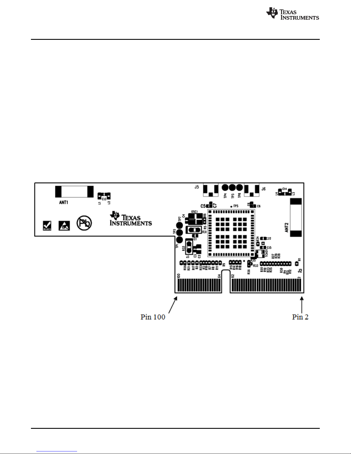
Figure 2 shows the top view of the EVB.
www.ti.com
4
WL1837MODCOM8I WLAN MIMO and Bluetooth®Module Evaluation Board SWRU382–November 2014
for TI Sitara™ Platform
Figure 2. EVB Top View
Copyright © 2014, Texas Instruments Incorporated
Submit Documentation Feedback
Page 5
www.ti.com
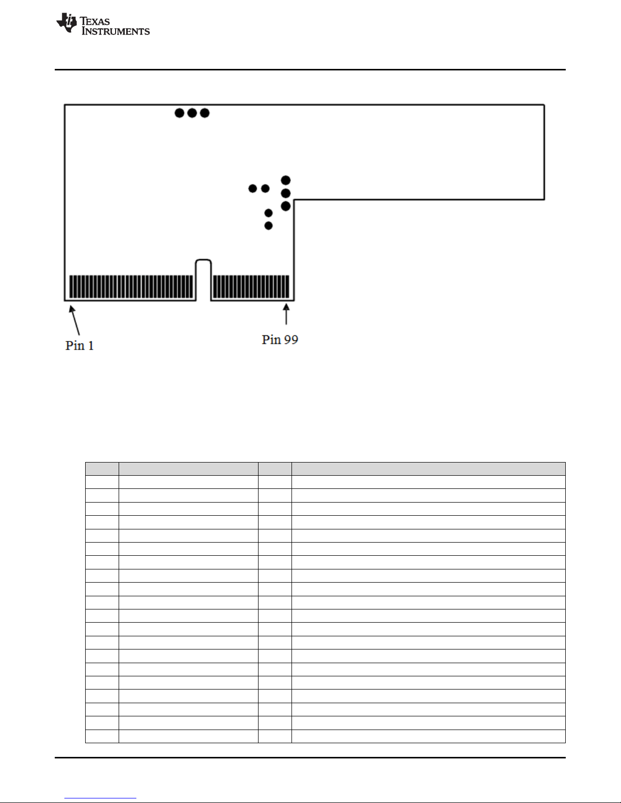
Figure 3 shows the bottom view of the EVB.
Board Pin Assignment
2.1 Pin Description
Table 1 describes the board pins.
No. Name Type Description
1 SLOW_CLK I Slow clock input option (default: NU)
2 GND G Ground
3 GND G Ground
4 WL_EN I WLAN enable
5 V
BAT
6 GND G Ground
7 V
BAT
8 V
IO
9 GND G Ground
10 N.C. No connection
11 WL_RS232_TX O WLAN tool RS232 output
12 N.C. No connection
13 WL_RS232_RX I WLAN tool RS232 input
14 N.C. No connection
15 WL_UART_DBG O WLAN Logger output
16 N.C. No connection
17 N.C. No connection
18 GND G Ground
19 GND G Ground
20 SDIO_CLK I WLAN SDIO clock
Figure 3. EVB (Bottom View)
Table 1. Pin Description
P 3.6-V typical voltage input
P 3.6-V typical voltage input
P VIO1.8-V (I/O voltage) input
SWRU382–November 2014 WL1837MODCOM8I WLAN MIMO and Bluetooth®Module Evaluation Board for
Submit Documentation Feedback
TI Sitara™ Platform
5
Copyright © 2014, Texas Instruments Incorporated
Page 6

Board Pin Assignment
No. Name Type Description
21 N.C. No connection
22 GND G Ground
23 N.C. No connection
24 SDIO_CMD I/O WLAN SDIO command
25 N.C. No connection
26 SDIO_D0 I/O WLAN SDIO data bit 0
27 N.C. No connection
28 SDIO_D1 I/O WLAN SDIO data bit 1
29 N.C. No connection
30 SDIO_D2 I/O WLAN SDIO data bit 2
31 N.C. No connection
32 SDIO_D3 I/O WLAN SDIO data bit 3
33 N.C. No connection
34 WLAN_IRQ O WLAN SDIO interrupt out
35 N.C. No connection
36 N.C. No connection
37 GND G Ground
38 N.C. No connection
39 N.C. No connection
40 N.C. No connection
41 N.C. No connection
42 GND G Ground
43 N.C. No connection
44 N.C. No connection
45 N.C. No connection
46 N.C. No connection
47 GND G Ground
48 N.C. No connection
49 N.C. No connection
50 N.C. No connection
51 N.C. No connection
52 PCM_IF_CLK I/O Bluetooth PCM clock input or output
53 N.C. No connection
54 PCM_IF_FSYNC I/O Bluetooth PCM frame sync input or output
55 N.C. No connection
56 PCM_IF_DIN I Bluetooth PCM data input
57 N.C. No connection
58 PCM_IF_DOUT O Bluetooth PCM data output
59 N.C. No connection
60 GND G Ground
61 N.C. No connection
62 N.C. No connection
63 GND G Ground
64 GND G Ground
65 N.C. No connection
66 BT_UART_IF_TX O Bluetooth HCI UART transmit output
67 N.C. No connection
www.ti.com
Table 1. Pin Description (continued)
6
WL1837MODCOM8I WLAN MIMO and Bluetooth®Module Evaluation Board for SWRU382–November 2014
TI Sitara™ Platform
Submit Documentation Feedback
Copyright © 2014, Texas Instruments Incorporated
Page 7

www.ti.com
Board Pin Assignment
Table 1. Pin Description (continued)
No. Name Type Description
68 BT_UART_IF_RX I Bluetooth HCI UART receive input
69 N.C. No connection
70 BT_UART_IF_CTS I Bluetooth HCI UART Clear-to-Send input
71 N.C. No connection
72 BT_UART_IF_RTS O Bluetooth HCI UART Request-to-Send output
73 N.C. No connection
74 RESERVED1 O Reserved
75 N.C. No connection
76 BT_UART_DEBUG O Bluetooth Logger UART output
77 GND G Ground
78 GPIO9 I/O General-purpose I/O
79 N.C. No connection
80 N.C. No connection
81 N.C. No connection
82 N.C. No connection
83 GND G Ground
84 N.C. No connection
85 N.C. No connection
86 N.C. No connection
87 GND G Ground
88 N.C. No connection
89 BT_EN I Bluetooth enable
90 N.C. No connection
91 N.C. No connection
92 GND G Ground
93 RESERVED2 I Reserved
94 N.C. No connection
95 GND G Ground
96 GPIO11 I/O General-purpose I/O
97 GND G Ground
98 GPIO12 I/O General-purpose I/O
99 TCXO_CLK_COM Option to supply 26 MHz externally
100 GPIO10 I/O General-purpose I/O
2.2 Jumper Connections
The WL1837MODCOM8I EVB includes the following jumper connections:
• J1: Jumper connector for VIOpower input
• J3: Jumper connector for V
• J5: RF connector for 2.4- and 5-GHz WLAN and Bluetooth
• J6: Second RF connector for 2.4-GHz WLAN
3 Electrical Characteristics
For electrical characteristics, see the WL18xxMOD WiLink™ Single-Band Combo Module – Wi-Fi®,
Bluetooth®, and Bluetooth Low Energy (BLE) Data Sheet (SWRS170).
SWRU382–November 2014 WL1837MODCOM8I WLAN MIMO and Bluetooth®Module Evaluation Board
Submit Documentation Feedback
power input
BAT
Copyright © 2014, Texas Instruments Incorporated
for TI Sitara™ Platform
7
Page 8

Antenna Characteristics
4 Antenna Characteristics
4.1 VSWR
Figure 4 shows the antenna VSWR characteristics.
www.ti.com
4.2 Efficiency
Figure 5 shows the antenna efficiency.
Figure 4. Antenna VSWR Characteristics
8
WL1837MODCOM8I WLAN MIMO and Bluetooth®Module Evaluation Board SWRU382–November 2014
for TI Sitara™ Platform
Figure 5. Antenna Efficiency
Copyright © 2014, Texas Instruments Incorporated
Submit Documentation Feedback
Page 9
EDGE CONNECTOR - MALE
ANT2 - WL_2.4_IO1/WL_5GHzANT1 - WL_2.4_IO2/BT/WL_5GHz
R20 for test mode.
These two TPs for test mode
when WL_IRQ pull high.
WL_UART_DBG
BT_AUD_CLK
BT_AUD_FSYNC
BT_AUD_IN
WL_RS232_TX
WL_RS232_RX
BT_HCI_TX
BT_HCI_RX
BT_HCI_CTS
BT_HCI_RTS
BT_EN_SOC
BT_UART_DBG
SDIO_CLK_WL
SDIO_CMD_WL
SDIO_D0_WL
SDIO_D2_WL
SDIO_D3_WL
SDIO_D1_WL
WLAN_EN_SOC
BT_AUD_OUT
BT_FUNC1
GPIO9
GPIO11
GPIO12
GPIO10
SLOW_CLK
BT_FUNC2
WLAN_IRQ
RF_ANT1 RF_ANT2
SDIO_D3_WL
GPIO12
SDIO_D2_WL
GPIO11
SDIO_D0_WL
SDIO_D1_WL
GPIO9
WLAN_IRQ
GPIO10
RF_ANT2
WL_RS232_TX
WL_RS232_RX
RF_ANT1
BT_FUNC1
BT_FUNC2
BT_HCI_RX
BT_HCI_TX
BT_HCI_CTS
BT_HCI_RTS
BT_AUD_IN
BT_AUD_OUT
BT_AUD_CLK
BT_AUD_FSYNC
SDIO_CMD_WL
SDIO_CLK_WL
SLOW_CLK
WL_UART_DBG
BT_UART_DBG
BT_EN_SOC
WLAN_EN_SOC
EXT_CLK_REQ_OUT
EXT_CLK_REQ_OUT
TCXO_CLK_COM
TCXO_CLK_COM
VBAT_IN
VIO_IN
VIO_IN
VBAT_IN
VIO_IN
VIO_IN
VBAT_IN VIO_CLK
VIO_CLK
R20 10k
0402
L3
2.2nH
0402
R25 0R 0402
C5
0R
0402
J6
U.FL-R-SMT(10)
U.FL
1
2
3
TCXO1
NU_TCXO 26MHz
2.0x1.6x0.73mm
NC
1
VCC4OUT
3
GND
2
R17
0R 0402
C6
0R
0402
R31
0R
0603
J2
NU_100pin Micro Edge MEC6
SD-100P
1 2
3 4
5 6
7 8
9 10
11 12
13 14
15 16
17 18
19 20
21 22
23 24
25 26
27 28
29 30
31 32
33 34
35 36
37 38
39 40
41 42
43 44
45 46
47 48
49 50
51 52
53 54
55 56
57 58
59 60
61 62
63 64
65 66
67 68
69 70
71 72
73 74
75 76
77 78
79 80
81 82
83 84
85 86
87 88
89 90
91 92
93 94
95 96
97 98
99 100
ANT1
W3006
ANT-10.0X3.2MM_B
FEED1NC
2
R33
0R
0402
TP4
1
C7
NU_0R
0402
U4
NU_TLV70518
XBGA-N4_0.8X0.8_0.4
VINB2VOUT
B1
ENA2GND
A1
R12 0R 0402
R11 0R 0402
R34
NU
0402
C1
1uF
0402
R30 0R 0402
R9 0R 0402
J5
U.FL-R-SMT(10)
U.FL
1
2
3
L2
NU
0402
R10 0R
0402
TP1
1
TP5
1
R2 0R 0402
L1
1.3nH
0402
0RR21 0402
0RR19 0402
OSC1
1V8 / 32.768kHz
OSC-3.2X2.5
EN
1
VCC
4
OUT
3
GND
2
R6
0R
0402
C32
NU_0.1uF
0402
R3 0R 0402
R16 0R 0402
U1
WL1837MODGJ
E-13.4X13.3-N100_0.75-TOP
GND
17
VIO
38
VBAT
47
EXT_32K
36
BT_AUD_FSYNC
58
BT_AUD_IN
56
BT_AUD_OUT
57
BT_AUD_CLK
60
WL_SDIO_D212WL_SDIO_CLK
8
WL_SDIO_D313WL_SDIO_D010WL_SDIO_D1
11
WL_SDIO_CMD
6
BT_HCI_RTS
50
BT_HCI_RX
53
BT_HCI_TX
52
BT_HCI_CTS
51
GND
16
GPIO_4
25
GPIO_2
26
GPIO_1
27
BT_EN_SOC
41
WLAN_IRQ
14
WLAN_EN_SOC
40
BT_UART_DBG
43
WL_UART_DBG
42
GND
G13
GND
G14
GND
G15
GND
G16
GND
G9
GND
G10
GND
48
GND
G11
GND
G12
VBAT
46
GND
28
GND
G1
GND
G2
GND
G3
GND
G4
GND
G5
GND
G6
GND
G7
GND
G8
RF_ANT1
32
RESERVED
64
GND
1
GND
20
RESERVED1
21
RESERVED2
22
GND
37
GND
19
RESERVED3
62
GND
G17
GND
G18
GND
G19
GND
G20
GND
G21
GND
G22
GND
G23
GND
G24
GND
G25
GND
G26
GND
G27
GND
G28
GND
G29
GND
G30
GND
G31
GND
G32
GND
G33
GND
G34
GND
G35
GND
23
GND
59
GND
34
GND
29
GND
7
RF_ANT2
18
GND
49
GND
9
GND
31
GND
35
GND
15
GND
55
GND45GND
44
GND
30
GND
24
GND
63
GND
61
GND
39
GND
33
GND
54
GND
G36
GPIO112GPIO93GPIO104GPIO12
5
R35
NU
0402
C2
10uF
0603
R32
0R
0603
J1
NU_HEADER 1x2
H-1X2_2MM
1
2
R1 0R 0402
R29 0R 0402
R8 0R 0402
TP7
1
C13
0.9pF
0402
TP6
1
TP3
1
R28 0R 0402
0RR24 0402
R7 0R 0402
R14 0R 0402
C8
NU_0R
0402
C4
0.1uF
0402
R27 0R 0402
R13 0R 0402
R15 0R 0402
C3
0.1uF
0402
0RR22 0402
R18 0R 0402
R4 0R 0402
R23 0R 0402
C15
NU_1uF
0402
ANT2
W3006
ANT-10.0X3.2MM_A
FEED1NC
2
C14
1.5pF
0402
R5 NU
0402
J3
NU_HEADER 1x2
H-1X2_2MM
1
2
L4
3.9nH
0402
R36 NU
0402
TP8
1
0RR26 0402
TP2
1
www.ti.com
4.3 Radio Pattern
For information on the antenna radio pattern and other related information, see
productfinder.pulseeng.com/product/W3006.
5 Circuit Design
5.1 EVB Reference Schematics
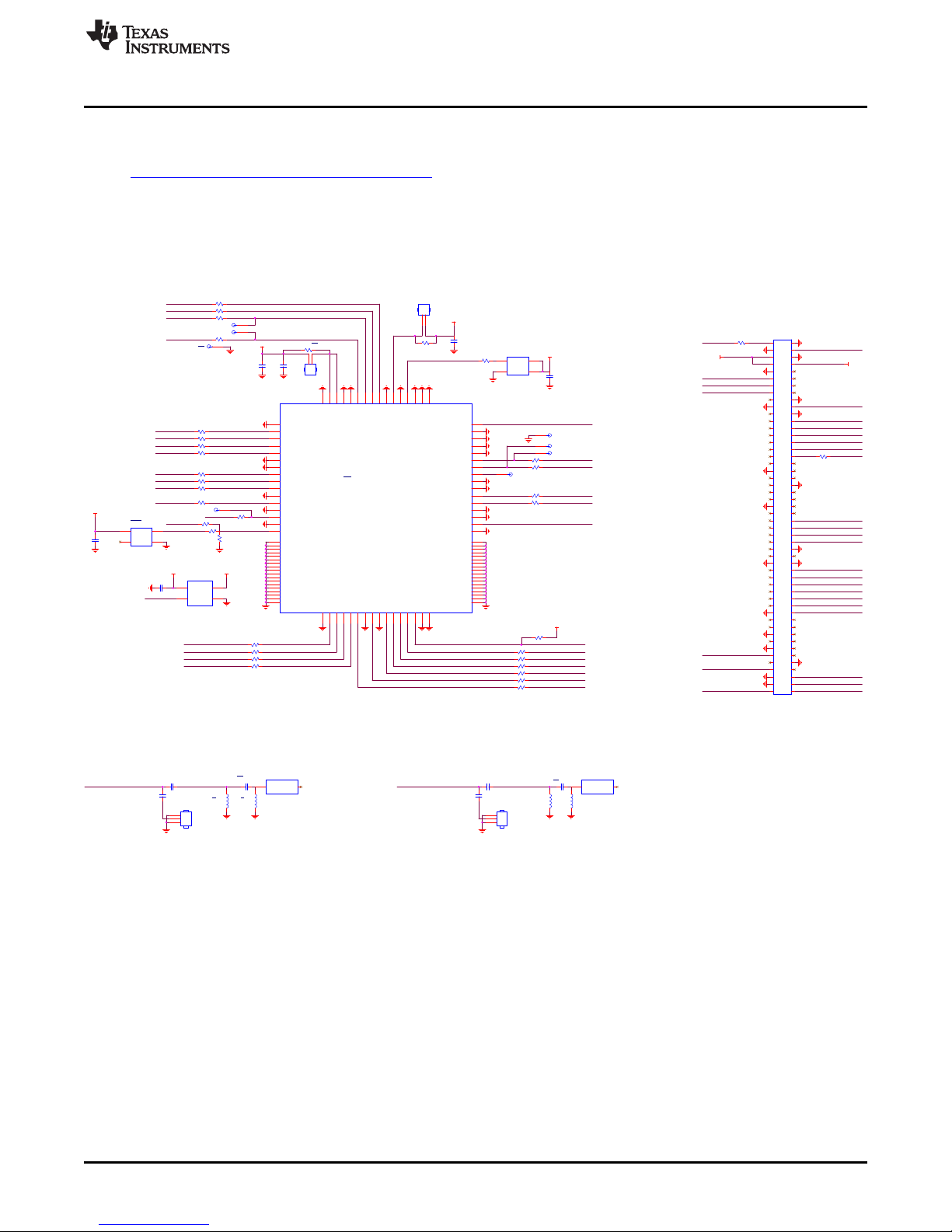
Figure 6 shows the reference schematics for the EVB.
Antenna Characteristics
Figure 6. EVB Reference Schematics
SWRU382–November 2014 WL1837MODCOM8I WLAN MIMO and Bluetooth®Module Evaluation Board
Submit Documentation Feedback
Copyright © 2014, Texas Instruments Incorporated
for TI Sitara™ Platform
9
Page 10

Circuit Design
5.2 Bill of Materials (BOM)
Table 2 lists the BOM for the EVB.
Item Description Part Number Package Reference Qty Mfr
1 TI WL1837 Wi-Fi / Bluetooth WL1837MODGI 13.4 mm x 13.3 mm U1 1 Jorjin
module x 2.0 mm
2 XOSC 3225 / 32.768KHZ / 1.8 V / 7XZ3200005 3.2 mm × 2.5 mm × OSC1 1 TXC
±50 ppm 1.0 mm
3 Antenna / Chip / 2.4 and 5 GHz W3006 10.0 mm × 3.2 mm ANT1, ANT2 2 Pulse
4 Mini RF header receptacle U.FL-R-SMT-1(10) 3.0 mm × 2.6 mm × J5, J6 2 Hirose
5 Inductor 0402 / 1.3 nH / ±0.1 nH / LQP15MN1N3B02 0402 L1 1 Murata
SMD
6 Inductor 0402 / 1.8 nH / ±0.1 nH / LQP15MN1N8B02 0402 L3 1 Murata
SMD
7 Inductor 0402 / 2.2 nH / ±0.1 nH / LQP15MN2N2B02 0402 L4 1 Murata
SMD
8 Capacitor 0402 / 1 pF / 50 V / C0G GJM1555C1H1R0BB01 0402 C13 1 Murata
/ ±0.1 pF
9 Capacitor 0402 / 2.4 pF / 50 V / GJM1555C1H2R4BB01 0402 C14 1 Murata
C0G / ±0.1 pF
10 Capacitor 0402 / 0.1 µF / 10 V / 0402B104K100CT 0402 C3, C4 2 Walsin
X7R / ±10%
11 Capacitor 0402 / 1 µF / 6.3 V / GRM155R60J105KE19D 0402 C1 1 Murata
X5R / ±10% / HF
12 Capacitor 0603 / 10 µF / 6.3 V / C1608X5R0J106M 0603 C2 1 TDK
X5R / ±20%
13 Resistor 0402 / 0R / ±5% WR04X000 PTL 0402 R1 to R4, R6 to 31 Walsin
14 Resistor 0402 / 10K / ±5% WR04X103 JTL 0402 R20 1 Walsin
15 Resistor 0603 / 0R / ±5% WR06X000 PTL 0603 R31, R32 2 Walsin
16 PCB WG7837TEC8B D02 / Layer 76.0 mm × 31.0 mm 1 茂榮
4 / FR4 (4 pcs / PNL) × 1.6 mm
(1)
C5 and C6 are mounted with a 0-Ω resistor by default.
Table 2. BOM
× 1.5 mm
1.25 mm
R19, R21 to
R30, R33, C5,
(1)
C6
www.ti.com
10
WL1837MODCOM8I WLAN MIMO and Bluetooth®Module Evaluation Board SWRU382–November 2014
for TI Sitara™ Platform
Copyright © 2014, Texas Instruments Incorporated
Submit Documentation Feedback
Page 11

www.ti.com
6 Layout Guidelines
6.1 Board Layout
Figure 7 through Figure 10 show the four layers of the WL1837MODCOM8I EVB.
Layout Guidelines
Figure 7. WL1837MODCOM8I Layer 1 Layout
Figure 8. WL1837MODCOM8I Layer 2 Layout
SWRU382–November 2014 WL1837MODCOM8I WLAN MIMO and Bluetooth®Module Evaluation Board
Submit Documentation Feedback
Copyright © 2014, Texas Instruments Incorporated
for TI Sitara™ Platform
11
Page 12

Layout Guidelines
www.ti.com
Figure 9. WL1837MODCOM8I Layer 3 Layout
Figure 10. WL1837MODCOM8I Layer 4 Layout
Figure 11 and Figure 12 show instances of good layout practices.
12
WL1837MODCOM8I WLAN MIMO and Bluetooth®Module Evaluation Board SWRU382–November 2014
for TI Sitara™ Platform
Copyright © 2014, Texas Instruments Incorporated
Submit Documentation Feedback
Page 13

www.ti.com
Layout Guidelines
Figure 11. Module Layout Guidelines (Top Layer)
Figure 12. Module Layout Guidelines (Bottom Layer)
Table 3 describes the guidelines corresponding to the reference numbers in Figure 11 and Figure 12.
Reference Guideline Description
1 Keep the proximity of ground vias close to the pad.
2 Do not run signal traces underneath the module on the layer where the module is mounted.
3 Have a complete ground pour in layer 2 for thermal dissipation.
4 Ensure a solid ground plane and ground vias under the module for stable system and thermal dissipation.
5 Increase ground pour in the first layer and have all traces from the first layer on the inner layers, if possible.
6 Signal traces can be run on a third layer under the solid ground layer and the module mounting layer.
SWRU382–November 2014 WL1837MODCOM8I WLAN MIMO and Bluetooth®Module Evaluation Board for
Submit Documentation Feedback
Table 3. Module Layout Guidelines
13
TI Sitara™ Platform
Copyright © 2014, Texas Instruments Incorporated
Page 14

Layout Guidelines
Figure 13 shows the trace design for the PCB. TI recommends using a 50-Ω impedance match on the
trace to the antenna and 50-Ω traces for the PCB layout.
Figure 14 shows layer 1 with the trace to the antenna over ground layer 2.
www.ti.com
Figure 13. Trace Design for the PCB Layout
Figure 14. Layer 1 Combined With Layer 2
Figure 15 and Figure 16 show instances of good layout practices for the antenna and RF trace routing.
NOTE: RF traces must be as short as possible. The antenna, RF traces, and modules must be on
the edge of the PCB product. The proximity of the antenna to the enclosure and the
enclosure material must also be considered.
14
WL1837MODCOM8I WLAN MIMO and Bluetooth®Module Evaluation Board SWRU382–November 2014
for TI Sitara™ Platform
Copyright © 2014, Texas Instruments Incorporated
Submit Documentation Feedback
Page 15

www.ti.com
Layout Guidelines
Figure 15. Top Layer – Antenna and RF Trace Routing Layout Guidelines
Figure 16. Bottom Layer – Antenna and RF Trace Routing Layout Guidelines
Table 4 describes the guidelines corresponding to the reference numbers in Figure 15 and Figure 16.
Table 4. Antenna and RF Trace Routing Layout Guidelines
Reference Guideline Description
1
2
3 RF traces must have via stitching on the ground plane beside the RF trace on both sides.
4 RF traces must have constant impedance (microstrip transmission line).
5
6 There must be no traces or ground under the antenna section.
SWRU382–November 2014 WL1837MODCOM8I WLAN MIMO and Bluetooth®Module Evaluation Board
Submit Documentation Feedback
The RF trace antenna feed must be as short as possible beyond the ground reference. At this point, the trace
starts to radiate.
RF trace bends must be gradual with an approximate maximum bend of 45 degrees with trace mitered. RF
traces must not have sharp corners.
For best results, the RF trace ground layer must be the ground layer immediately below the RF trace. The
ground layer must be solid.
Copyright © 2014, Texas Instruments Incorporated
for TI Sitara™ Platform
15
Page 16
Ordering Information
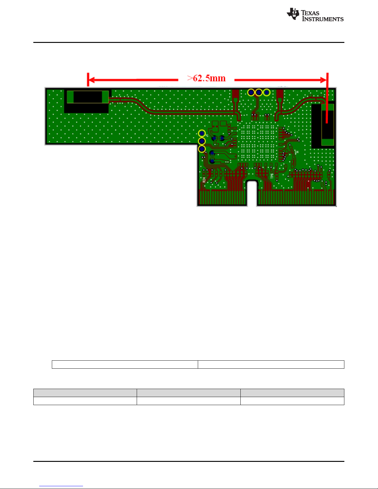
Figure 17 shows the MIMO antenna spacing. The distance between ANT1 and ANT2 must be greater
than half the wavelength (62.5 mm at 2.4 GHz).
www.ti.com
Follow these supply routing guidelines:
• For power supply routing, the power trace for V
• The 1.8-V trace must be at least 18-mil wide.
• Make V
traces as wide as possible to ensure reduced inductance and trace resistance.
BAT
• If possible, shield V
Follow these digital-signal routing guidelines:
• Route SDIO signal traces (CLK, CMD, D0, D1, D2, and D3) in parallel to each other and as short as
possible (less than 12 cm). In addition, each trace must be the same length. Ensure enough space
between traces (greater than 1.5 times the trace width or ground) to ensure signal quality, especially
for the SDIO_CLK trace. Remember to keep these traces away from the other digital or analog signal
traces. TI recommends adding ground shielding around these buses.
• Digital clock signals (SDIO clock, PCM clock, and so on) are a source of noise. Keep the traces of
these signals as short as possible. Whenever possible, maintain a clearance around these signals.
7 Ordering Information
Part number: WL1837MODCOM8I
DATE REVISION NOTES
November 2014 * Initial draft
Figure 17. MIMO Antenna Spacing
must be at least 40-mil wide.
BAT
traces with ground above, below, and beside the traces.
BAT
Revision History
16
Revision History SWRU382–November 2014
Copyright © 2014, Texas Instruments Incorporated
Submit Documentation Feedback
Page 17

IMPORTANT NOTICE
Texas Instruments Incorporated and its subsidiaries (TI) reserve the right to make corrections, enhancements, improvements and other
changes to its semiconductor products and services per JESD46, latest issue, and to discontinue any product or service per JESD48, latest
issue. Buyers should obtain the latest relevant information before placing orders and should verify that such information is current and
complete. All semiconductor products (also referred to herein as “components”) are sold subject to TI’s terms and conditions of sale
supplied at the time of order acknowledgment.
TI warrants performance of its components to the specifications applicable at the time of sale, in accordance with the warranty in TI’s terms
and conditions of sale of semiconductor products. Testing and other quality control techniques are used to the extent TI deems necessary
to support this warranty. Except where mandated by applicable law, testing of all parameters of each component is not necessarily
performed.
TI assumes no liability for applications assistance or the design of Buyers’ products. Buyers are responsible for their products and
applications using TI components. To minimize the risks associated with Buyers’ products and applications, Buyers should provide
adequate design and operating safeguards.
TI does not warrant or represent that any license, either express or implied, is granted under any patent right, copyright, mask work right, or
other intellectual property right relating to any combination, machine, or process in which TI components or services are used. Information
published by TI regarding third-party products or services does not constitute a license to use such products or services or a warranty or
endorsement thereof. Use of such information may require a license from a third party under the patents or other intellectual property of the
third party, or a license from TI under the patents or other intellectual property of TI.
Reproduction of significant portions of TI information in TI data books or data sheets is permissible only if reproduction is without alteration
and is accompanied by all associated warranties, conditions, limitations, and notices. TI is not responsible or liable for such altered
documentation. Information of third parties may be subject to additional restrictions.
Resale of TI components or services with statements different from or beyond the parameters stated by TI for that component or service
voids all express and any implied warranties for the associated TI component or service and is an unfair and deceptive business practice.
TI is not responsible or liable for any such statements.
Buyer acknowledges and agrees that it is solely responsible for compliance with all legal, regulatory and safety-related requirements
concerning its products, and any use of TI components in its applications, notwithstanding any applications-related information or support
that may be provided by TI. Buyer represents and agrees that it has all the necessary expertise to create and implement safeguards which
anticipate dangerous consequences of failures, monitor failures and their consequences, lessen the likelihood of failures that might cause
harm and take appropriate remedial actions. Buyer will fully indemnify TI and its representatives against any damages arising out of the use
of any TI components in safety-critical applications.
In some cases, TI components may be promoted specifically to facilitate safety-related applications. With such components, TI’s goal is to
help enable customers to design and create their own end-product solutions that meet applicable functional safety standards and
requirements. Nonetheless, such components are subject to these terms.
No TI components are authorized for use in FDA Class III (or similar life-critical medical equipment) unless authorized officers of the parties
have executed a special agreement specifically governing such use.
Only those TI components which TI has specifically designated as military grade or “enhanced plastic” are designed and intended for use in
military/aerospace applications or environments. Buyer acknowledges and agrees that any military or aerospace use of TI components
which have not been so designated is solely at the Buyer's risk, and that Buyer is solely responsible for compliance with all legal and
regulatory requirements in connection with such use.
TI has specifically designated certain components as meeting ISO/TS16949 requirements, mainly for automotive use. In any case of use of
non-designated products, TI will not be responsible for any failure to meet ISO/TS16949.
Products Applications
Audio www.ti.com/audio Automotive and Transportation www.ti.com/automotive
Amplifiers amplifier.ti.com Communications and Telecom www.ti.com/communications
Data Converters dataconverter.ti.com Computers and Peripherals www.ti.com/computers
DLP® Products www.dlp.com Consumer Electronics www.ti.com/consumer-apps
DSP dsp.ti.com Energy and Lighting www.ti.com/energy
Clocks and Timers www.ti.com/clocks Industrial www.ti.com/industrial
Interface interface.ti.com Medical www.ti.com/medical
Logic logic.ti.com Security www.ti.com/security
Power Mgmt power.ti.com Space, Avionics and Defense www.ti.com/space-avionics-defense
Microcontrollers microcontroller.ti.com Video and Imaging www.ti.com/video
RFID www.ti-rfid.com
OMAP Applications Processors www.ti.com/omap TI E2E Community e2e.ti.com
Wireless Connectivity www.ti.com/wirelessconnectivity
Mailing Address: Texas Instruments, Post Office Box 655303, Dallas, Texas 75265
Copyright © 2014, Texas Instruments Incorporated
 Loading...