

Page 1

WL1835MODCOM8A WLAN MIMO and BT
Module Evaluation Board for TI Sitara™
Platform
User's Guide
Literature Number: SWRU359A
September 2013 –Revised October 2013
Page 2

Contents
Preface ....................................................................................................................................... 3
1 Introduction ........................................................................................................................ 4
1.1 Features .................................................................................................................. 4
1.2 Applications .............................................................................................................. 5
1.3 TI Module Key Benefits ................................................................................................. 5
2 Board Pin Assignment ......................................................................................................... 6
2.1 Pin Descriptions ......................................................................................................... 7
3 Electrical Characteristics ..................................................................................................... 9
4 Antenna Characteristics ....................................................................................................... 9
4.1 VSWR ..................................................................................................................... 9
4.2 Efficiency ................................................................................................................ 10
5 Antenna Characteristics ..................................................................................................... 10
5.1 Radio Pattern ........................................................................................................... 10
6 Circuit Design ................................................................................................................... 14
6.1 Schematic ............................................................................................................... 14
6.2 Bill of Materials (BOM) ................................................................................................ 15
7 Layout Guidelines ............................................................................................................. 16
7.1 Board Layout ........................................................................................................... 16
2
Table of Contents SWRU359A–September 2013–Revised October 2013
Copyright © 2013, Texas Instruments Incorporated
Submit Documentation Feedback
Page 3

About This Manual
This user's guide describes how to use the TI WL1835MODCOM8A board to evaluate the performance of
the TI WL1835MODGA module.
Related Documentation From Texas Instruments
• TI WiLink8 Single-Band Combo Module – Wi-Fi, BT, and BLE (SWRS152)
• WiLink 8 Wiki: http://www.ti.com/wilink8wiki
If You Need Assistance
The primary sources of WL1835MODGA information are the device-specific data sheets and user’s
guides. For the most up-to-date version of the user’s guide and data sheets, go to
http://www.ti.com/product/wl1835mod.
Warning
The WL1835MODCOM8A board is tested to comply with ETSI/R&TTE over temperatures from 0 to
+70°C. The WL1835MODCOM8A board is FCC and IC certified.
This board should not be modified to operate in other frequency bands other than what they are designed
for.
FCC/IC Regulatory compliance (WL1835MODCOM8A board only)
FCC Part 15 Class A Compliant
IC ICES-003 Class A Compliant
Preface
SWRU359A–September 2013–Revised October 2013
Read This First
SWRU359A–September 2013–Revised October 2013 Preface
Submit Documentation Feedback
3
Copyright © 2013, Texas Instruments Incorporated
Page 4
WL1835MODCOM8A WLAN MIMO and BT Module
1 Introduction
The WL1835MODCOM8A device is a WiFi®MIMO, Bluetooth®, and Bluetooth Low Energy (BLE) module
board with the TI WL1835MODGA module. WL1835MODGA is built-in TI WL1835 IEEE 802.11 b/g/n and
Bluetooth 4.0 solutions to provide the best WiFi and Bluetooth coexistence interoperability and power-
saving technologies from TI.
User's Guide
SWRU359A–September 2013–Revised October 2013
Evaluation Board for TI Sitara™ Platform
1.1 Features
• WLAN, Bluetooth, BLE on a module board
• 100-pin board card
• Dimension 76.0 mm(L) x 31.0 mm(W)
• WLAN 2.4 GHz SISO (20- and 40-MHz channels), 2.4-GHz MIMO (20-MHz channels)
• Support for BLE dual mode
• Seamless integration with TI Sitara and other application processors
• Design for TI AM335X general-purpose EVM
• WLAN and Bluetooth, BLE cores are software and hardware compatible with prior WL127x, WL128x
and CC256x offerings, for smooth migration to device.
• Shared HCI transport for Bluetooth and BLE over UART and SDIO for WLAN.
• WiFi / Bluetooth single antenna co-existence
• Built-in chip antenna
• Optional U.FL RF connector for external 2.4-GHz band antenna
• Direct connection to battery using external switching mode power supply supporting 4.8-V to 2.9-V
operation
• VIO in the 1.8-V domain
4
WL1835MODCOM8A WLAN MIMO and BT Module Evaluation Board for TI SWRU359A– September 2013 – Revised October 2013
Sitara™ Platform
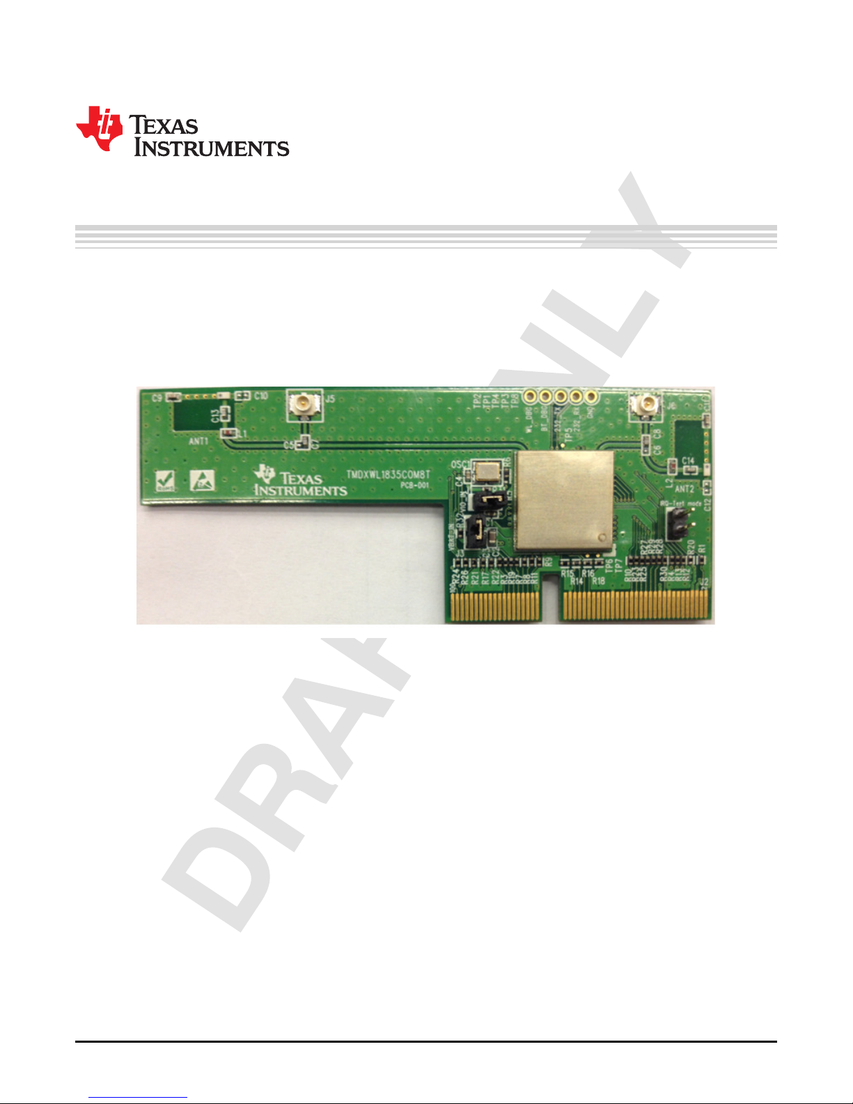
Figure 1. WL1835MODCOM8A Top View
Copyright © 2013, Texas Instruments Incorporated
Submit Documentation Feedback
Page 5

www.ti.com
1.2 Applications
• Internet of Things Multimedia
• Home Electronics
• Home Appliances and White Goods
• Industrial and Home Automation
• Smart Gateway and Metering
• Video Conferencing
• Video Camera and Security
1.3 TI Module Key Benefits
• Reduces Design Overhead: Single WiLink8™ Module Scales Across Wi-Fi and Bluetooth.
• WLAN High Throughput: 80 Mbps (TCP), 100 Mbps (UDP)
• Bluetooth 4.0 + BLE (Smart Ready)
• WiFi-Bluetooth Single Antenna Coexistence
• Low Power (30–50% Less than Previous Generation)
• Available as Easy-to-Use FCC, ETSI, and Telec Certified Module
• Lower Manufacturing Costs, Saving Board Space and Minimizing RF Expertise
• AM335x Linux®and Android™ Reference Platform Accelerates Customer Development and Time to
Market
Introduction
SWRU359A–September 2013–Revised October 2013 WL1835MODCOM8A WLAN MIMO and BT Module Evaluation Board for TI
Submit Documentation Feedback
Copyright © 2013, Texas Instruments Incorporated
Sitara™ Platform
5
Page 6
Board Pin Assignment
2 Board Pin Assignment
www.ti.com
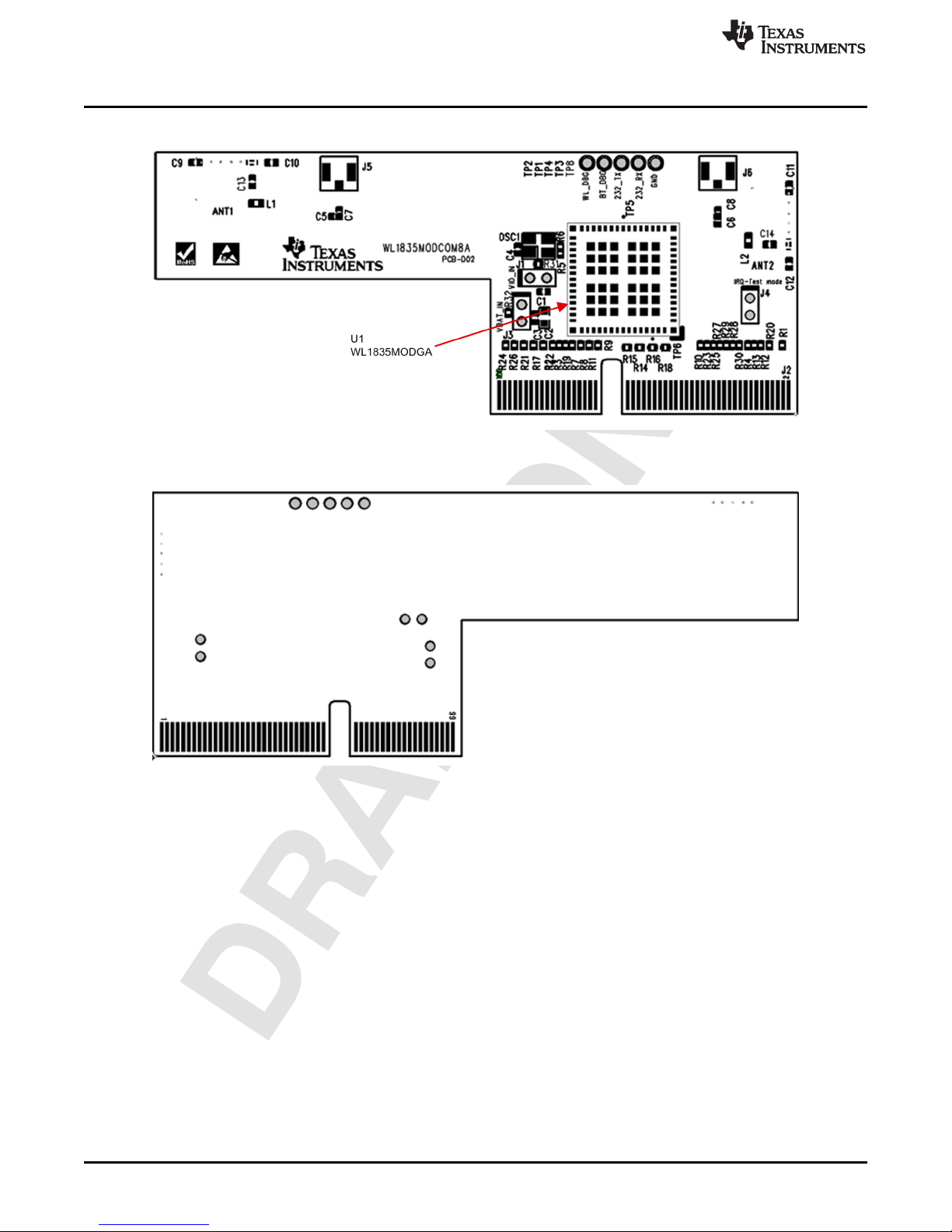
Figure 2. Board Top View
6
WL1835MODCOM8A WLAN MIMO and BT Module Evaluation Board for TI SWRU359A– September 2013 – Revised October 2013
Sitara™ Platform
Figure 3. Board Bottom View
Copyright © 2013, Texas Instruments Incorporated
Submit Documentation Feedback
Page 7

www.ti.com
2.1 Pin Descriptions
No. Name Type Description
1 SLOW_CLK I Slow clock input
2 GND G Ground
3 GND G Ground
4 WL_EN I WLAN Enable
5 VBAT P Power supply input
6 GND G Ground
7 VBAT P Power supply input
8 VIO P Power supply input for I/O pin
9 GND G Ground
10 N.C. No connection
11 WL_RS232_TX O WLAN tool RS232 output
12 N.C. No connection
13 WL_RS232_RX I WLAN tool RS232 input
14 N.C. No connection
15 WL_UART_DBG O WLAN Logger output
16 N.C. No connection
17 N.C. No connection
18 GND G Ground
19 GND G Ground
20 SDIO_CLK I WLAN SDIO clock
21 N.C. No connection
22 GND G Ground
23 N.C. No connection
24 SDIO_CMD I/O WLAN SDIO command
25 N.C. No connection
26 SDIO_D0 I/O WLAN SDIO data bit 0
27 N.C. No connection
28 SDIO_D1 I/O WLAN SDIO data bit 1
29 N.C. No connection
30 SDIO_D2 I/O WLAN SDIO data bit 2
31 N.C. No connection
32 SDIO_D3 I/O WLAN SDIO data bit 3
33 N.C. No connection
34 WLAN_IRQ O WLAN SDIO interrupt out
35 N.C. No connection
36 N.C. No connection
37 GND G Ground
38 N.C. No connection
39 N.C. No connection
40 N.C. No connection
41 N.C. No connection
42 GND G Ground
43 N.C. No connection
44 N.C. No connection
45 N.C. No connection
46 N.C. No connection
47 GND G Ground
Board Pin Assignment
SWRU359A–September 2013–Revised October 2013 WL1835MODCOM8A WLAN MIMO and BT Module Evaluation Board for TI
Submit Documentation Feedback
Sitara™ Platform
7
Copyright © 2013, Texas Instruments Incorporated
Page 8

Board Pin Assignment
No. Name Type Description
48 N.C. No connection
49 N.C. No connection
50 N.C. No connection
51 N.C. No connection
52 PCM_IF_CLK I/O Bluetooth PCM clock input or output
53 N.C. No connection
54 PCM_IF_FSYNC I/O Bluetooth PCM frame sync input or output
55 N.C. No connection
56 PCM_IF_DIN I Bluetooth PCM data input
57 N.C. No connection
58 PCM_IF_DOUT O Bluetooth PCM data output
59 N.C. No connection
60 GND G Ground
61 N.C. No connection
62 N.C. No connection
63 GND G Ground
64 GND G Ground
65 N.C. No connection
66 BT_UART_IF_TX O Bluetooth HCI UART transmit output
67 N.C. No connection
68 BT_UART_IF_RX I Bluetooth HCI UART receive input
69 N.C. No connection
70 BT_UART_IF_CTS I Bluetooth HCI UART Clear to Send input
71 N.C. No connection
72 BT_UART_IF_RTS O Bluetooth HCI UART Request to Send output
73 N.C. No connection
74 BT_FUNC1 O BT_HOST_WAKE_UP Signal to wake up the host from Bluetooth
75 N.C. No connection
76 BT_UART_DEBUG O Bluetooth Logger UART output
77 GND G Ground
78 GPIO9 I/O General-purpose I/O
79 N.C. No connection
80 N.C. No connection
81 N.C. No connection
82 N.C. No connection
83 GND G Ground
84 N.C. No connection
85 N.C. No connection
86 N.C. No connection
87 GND G Ground
88 N.C. No connection
89 BT_EN I Bluetooth Enable
90 N.C. No connection
91 N.C. No connection
92 GND G Ground
93 BT_FUNC2 I BT_WAKE_UP Bluetooth wakeup from host
94 N.C. No connection
95 GND G Ground
96 GPIO11 I/O General-purpose I/O
www.ti.com
8
WL1835MODCOM8A WLAN MIMO and BT Module Evaluation Board for TI SWRU359A – September 2013 – Revised October 2013
Sitara™ Platform
Submit Documentation Feedback
Copyright © 2013, Texas Instruments Incorporated
Page 9

www.ti.com
No. Name Type Description
97 GND G Ground
98 GPIO12 I/O General-purpose I/O
99 N.C. General-purpose I/O
100 GPIO10 I/O General-purpose I/O
3 Electrical Characteristics
Refer to the detailed data in the WL1835MODGA data sheet for electrical characteristics.
4 Antenna Characteristics
4.1 VSWR
Figure 4 shows the antenna VSWR.
Electrical Characteristics
SWRU359A–September 2013–Revised October 2013 WL1835MODCOM8A WLAN MIMO and BT Module Evaluation Board for TI
Submit Documentation Feedback
Figure 4. Antenna VSWR
Copyright © 2013, Texas Instruments Incorporated
Sitara™ Platform
9
Page 10

Antenna Characteristics
4.2 Efficiency
Figure 5 shows the antenna efficiency.
www.ti.com
5 Antenna Characteristics
5.1 Radio Pattern
Figure 6 shows the radio pattern of the WL1835MODCOM8A device.
Figure 5. Antenna Efficiency
10
WL1835MODCOM8A WLAN MIMO and BT Module Evaluation Board for TI SWRU359A– September 2013 – Revised October 2013
Sitara™ Platform
Figure 6.
Copyright © 2013, Texas Instruments Incorporated
Submit Documentation Feedback
Page 11

www.ti.com
5.1.1 ANT1
Figure 7 shows the ANT1 polarization of the WL1835MODCOM8A device.
Antenna Characteristics
Figure 7.
SWRU359A–September 2013–Revised October 2013 WL1835MODCOM8A WLAN MIMO and BT Module Evaluation Board for TI
Submit Documentation Feedback
Figure 8.
Copyright © 2013, Texas Instruments Incorporated
Sitara™ Platform
11
Page 12

Antenna Characteristics
5.1.2 ANT2
Figure 10 shows the ANT2 polarization of the WL1835MODCOM8A device.
www.ti.com
Figure 9.
12
WL1835MODCOM8A WLAN MIMO and BT Module Evaluation Board for TI SWRU359A– September 2013 – Revised October 2013
Sitara™ Platform
Figure 10.
Copyright © 2013, Texas Instruments Incorporated
Submit Documentation Feedback
Page 13

www.ti.com
Antenna Characteristics
Figure 11.
SWRU359A–September 2013–Revised October 2013 WL1835MODCOM8A WLAN MIMO and BT Module Evaluation Board for TI
Submit Documentation Feedback
Figure 12.
Copyright © 2013, Texas Instruments Incorporated
Sitara™ Platform
13
Page 14

U1
WL1835MODGA
E-13.4X13.3-N100_0.75-TOP
WL_BG ANT2WL_BG/BT ANT1
Short PIN Header (1-2)
for entering test mode.
Open for function mode.
These two TPs for test mode
when WL_IRQ pull high.
EDGE CONNECTOR - MALE
J5
U.FL-R-SMT(10)
U.FL
1
2
3
SDIO_CMD_WL
R28 0R 0402
J2
NU_100pin Micro Edge MEC6
SD-100P
1 2
3 4
5 6
7 8
9 10
11 12
13 14
15 16
17 18
19 20
21 22
23 24
25 26
27 28
29 30
31 32
33 34
35 36
37 38
39 40
41 42
43 44
45 46
47 48
49 50
51 52
53 54
55 56
57 58
59 60
61 62
63 64
65 66
67 68
69 70
71 72
73 74
75 76
77 78
79 80
81 82
83 84
85 86
87 88
89 90
91 92
93 94
95 96
97 98
99 100
R30 0R
0402
SDIO_CLK_WL
ANT2
ANT016008LCD2442MA1
ANT-N3-1.6X0.8MM-B
5G
B2
FEED
A
2.4G
B1
R10 0R
0402
ANT1
ANT016008LCD2442MA1
ANT-N3-1.6X0.8MM-A
5G
B2
FEED
A
2.4G
B1
WLAN_EN_SOC
C12
NU
0402
L1
0402
1.1nH
C8
NU_10pF
0402
R5 NU_0R
0402
J6
U.FL-R-SMT(10)
U.FL
1
2
3
L2
1.5nH
0402
GPIO93GPIO125GPIO112GPIO10
4
GND
17
VIO
38
VBAT
47
EXT_32K
36
BT_AUD_FSYN C
58
BT_AUD_IN
56
BT_AUD_OUT
57
BT_AUD_CLK
60
WL_SDIO_D2
12
WL_SDIO_CLK8WL_SDIO_D313WL_SDIO_D010WL_SDIO_D1
11
WL_SDIO_CM D
6
BT_HCI_RTS
50
BT_HCI_RX
53
BT_HCI_TX
52
BT_HCI_CTS
51
GND
16
GPIO_4
25
GPIO_2
26
GPIO_1
27
BT_EN_SOC
41
WLAN_IRQ
14
WLAN_EN_SOC
40
BT_UART_D BG
43
WL_UART_D BG
42
GND
G13
GND
G14
GND
G15
GND
G16
GND
G9
GND
G10
GND
48
GND
G11
GND
G12
VBAT
46
GND
28
GND
G1
GND
G2
GND
G3
GND
G4
GND
G5
GND
G6
GND
G7
GND
G8
2G4_ANT1_WB
32
GND
64
GND
1
GND
20
RESERVED1
21
RESERVED2
22
GND
37
GND
19
RESERVED3
62
GND
G17
GND
G18
GND
G19
GND
G20
GND
G21
GND
G22
GND
G23
GND
G24
GND
G25
GND
G26
GND
G27
GND
G28
GND
G29
GND
G30
GND
G31
GND
G32
GND
G33
GND
G34
GND
G35
GND
23
GND
59
GND
34
GND
29
GND
7
2G4_ANT2_W
18
GND
49
GND
9
GND
31
GND
35
GND
15
GND
55
GND45GND
44
GND
30
GND
24
GND
63
GND
61
GND
39
GND
33
GND
54
GND
G36
C5
10pF
0402
C6
10pF
0402
C11
1.2pF
0402
C14
4pF
0402
C10
NU_0.3pF
0402
C9
2pF
0402
VBAT_IN
VIO_IN
BT_FUNC1
C4
0.1uF
0402
C3
0.1uF
0402
R4 0R 0402
J3
HEADER 1x2
H-1X2_2MM
1
2
SLOW_CLK
TP2
1
TP8
1
R6
0R
0402
TP1
1
OSC1
1V8 / 32.768k Hz
OSC-3.2X2.5
EN
1
VCC
4
OUT
3
GND
2
R3 0R 0402
J1
HEADER 1x2
H-1X2_2MM
1
2
VBAT_IN
VIO_IN
VIO_IN
WL_UART_DBG
C1
1uF
0402
BT_UART_DBG
BT_EN_SOC
WLAN_EN_SOC
R31
0R
0402
R32
0R
0402
R2 0R0402
GPIO10
C2
10uF
0603
R1 0R0402
R29 0R 0402
0RR24 0402
R27 0R 0402
0RR22 0402 R23 0R 0402
J4
HEADER 1x2
H-1X2_2MM
1
2
0RR26 0402
R20 10k
0402
R25 0R 0402
SDIO_D3_WL
GPIO12
SDIO_D2_WL
GPIO11
SDIO_D0_WL
SDIO_D1_WL
GPIO9
WLAN_IRQ
GPIO10
VIO_IN
0RR21 0402
BT_FUNC2
GPIO9
2G4_ANT2_W
R17 0R 0402
TP5
1
R12 0R 0402
WL_RS232_TX
TP4
1
WL_RS232_RX
2G4_ANT1_WB
BT_FUNC1
BT_FUNC2
R13 0R 0402
TP3
1
0RR19 0402
2G4_ANT2_W
WLAN_IRQ
GPIO11
BT_AUD_CLK
BT_AUD_FSYN C
BT_AUD_IN
WL_RS232_TX
WL_RS232_RX
BT_HCI_TX
BT_HCI_RX
BT_HCI_CTS
BT_HCI_RTS
BT_EN_SOC
BT_UART_DBG
SDIO_CLK_WL
SDIO_CMD_WL
SDIO_D0_WL
SDIO_D2_WL
SDIO_D3_WL
SDIO_D1_WL
C13
8pF
0402
GPIO12
R14 0R 0402
R15 0R 0402
R18 0R 0402
R16 0R 0402
TP6
1
R11 0R 0402
BT_HCI_RX
R9 0R 0402
BT_HCI_TX
BT_HCI_CTS
BT_HCI_RTS
BT_AUD_IN
BT_AUD_OUT
BT_AUD_CLK
BT_AUD_FSYN C
R8 0R 0402
R7 0R 0402
2G4_ANT1_WB
BT_AUD_OUT
SLOW_CLK
C7
NU_10pF
0402
WL_UART_DBG
Circuit Design
www.ti.com
6 Circuit Design
6.1 Schematic
Figure 13. Schematic
14
WL1835MODCOM8A WLAN MIMO and BT Module Evaluation Board for TI SWRU359A–September 2013 –Revised October 2013
Sitara™ Platform
Submit Documentation Feedback
Copyright © 2013, Texas Instruments Incorporated
Page 15

www.ti.com
6.2 Bill of Materials (BOM)
Table 1 lists the bill of materials.
1 TI WL1835 WiFi/Bluetooth Module WL1835MODGA U1
2 XOSC 3225 / 32.768 kHz / 1.8 V / ±50 ppm 7XZ3200005 OSC1
3 ANT / Chip / 2.4 GHz, 5 GHz / Peak Gain >5 dBi ANT016008LCD2442MA1 ANT1, ANT2
4 CON Male 1x2 / Pitch P301-SGP-040/028-02 J1, J3, J4
5 DC JUMPER / PITCH 2.0 mm CMJ-20BB J1, J3
6 Mini RF Header Receptacle U.FL-R-SMT-1(10) J5, J6
7 IND 0402 / 1.1 nH / ±0.05 nH / SMD LQP15MN1N1W02 L1
8 IND 0402 / 1.5 nH / ±0.05 nH / SMD LQP15MN1N5W02 L2
9 CAP 0402 / 1.2 pF / 50 V / C0G / ±0.1 pF GJM1555C1H1R2BB01 C11
10 CAP 0402 / 2.2 pF / 50 V / C0G / ±0.1 pF GJM1555C1H2R2BB01 C9
11 CAP 0402 / 4 pF / 50 V / C0G / ±0.1 pF GJM1555C1H4R0BB01 C14
12 CAP 0402 / 8 pF / 50 V / C0G / ±0.1 pF GJM1555C1H8R0BB01 C13
13 CAP 0402 / 10 pF / 50 V / NPO / ±5% 0402N100J500LT C7, C8
14 CAP 0402 / 0.1 µF / 6.3 V / X7R / ±10% 0402B104K100CT C3, C4
15 CAP 0402 / 1 µF / 6.3 V / X5R / ±10% / HF GRM155R60J105KE19D C1
16 CAP 0603 / 10 µF / 6.3 V / X5R / ±20% C1608X5R0J106M C2
17 RES 0402 / 0R / ±5% WR04X000 PTL R16, R17, R18, R19, R21, R22,
18 RES 0402 / 10K / ±5% WR04X103 JTL R20
Circuit Design
Table 1. BOM
R1, R2, R3, R4, R5, R6, R7, R8, R9,
R10, R11, R12, R13, R14, R15,
R23, R24, R25, R26, R27, R28,
R29, R30, R31, R32
SWRU359A–September 2013–Revised October 2013 WL1835MODCOM8A WLAN MIMO and BT Module Evaluation Board for TI
Submit Documentation Feedback
Copyright © 2013, Texas Instruments Incorporated
Sitara™ Platform
15
Page 16

Layout Guidelines
7 Layout Guidelines
7.1 Board Layout
Figure 14 shows the WL1835MODCOM8A 4-layer board. Table 2, Figure 15, Figure 16, Figure 17,
Figure 18, and Figure 19 show instances of good layout practices.
www.ti.com
Figure 14. Layer 1
16
WL1835MODCOM8A WLAN MIMO and BT Module Evaluation Board for TI SWRU359A– September 2013 – Revised October 2013
Sitara™ Platform
Figure 15. Layer 2
Copyright © 2013, Texas Instruments Incorporated
Submit Documentation Feedback
Page 17

www.ti.com
Layout Guidelines
Figure 16. Layer 3
Reference Guideline Description
1 The proximity of ground vias must be close to the pad.
2 Signal traces must not be run underneath the module on the layer where the module is mounted.
3 Have a complete ground pour in layer 2 for thermal dissipation.
4 Have a solid ground plane and ground vias under the module for stable system and thermal dissipation.
5
6
SWRU359A–September 2013–Revised October 2013 WL1835MODCOM8A WLAN MIMO and BT Module Evaluation Board for TI
Submit Documentation Feedback
Increase the ground pour in the first layer and have all of the traces from the first layer on the inner layers, if
possible.
Signal traces can be run on a third layer under the solid ground layer, which is below the module mounting
layer.
Figure 17. Layer 4
Table 2. Module Layout Guidelines
Copyright © 2013, Texas Instruments Incorporated
Sitara™ Platform
17
Page 18

Layout Guidelines
www.ti.com
Figure 18. Module Layout Guidelines (Top Layer)
Figure 19. Module Layout Guidelines (Bottom Layer)
Figure 20 shows the trace design for the PCB. A 50-Ω impedance match on the trace to the antenna
should be used. Also, 50-Ω traces are recommended for the PCB layout.
18
WL1835MODCOM8A WLAN MIMO and BT Module Evaluation Board for TI SWRU359A– September 2013 – Revised October 2013
Sitara™ Platform
Copyright © 2013, Texas Instruments Incorporated
Submit Documentation Feedback
Page 19

www.ti.com
Figure 21 shows layer 1 with the trace to the antenna over ground layer 2.
Layout Guidelines
Figure 20. Trace Design for the PCB Layout
Table 3, Figure 22, and Figure 23 describe instances of good layout practices for the antenna and RF
trace routing.
Table 3. Antenna and RF Trace Routing Layout Guidelines
Reference Guideline Description
1
2
3 RF traces must have via stitching on the ground plane beside the RF trace on both sides
4 RF traces must have constant impedance (microstrip transmission line).
5
6 There must be no traces or ground under the antenna section.
7
SWRU359A–September 2013–Revised October 2013 WL1835MODCOM8A WLAN MIMO and BT Module Evaluation Board for TI
Submit Documentation Feedback
The RF trace antenna feed must be as short as possible beyond the ground reference. At this point, the trace
starts to radiate.
The RF trace bends must be gradual with an approximate maximum bend of 45 degrees with trace mitered. RF
traces must not have sharp corners.
For best results, the RF trace ground layer must be the ground layer immediately below the RF trace. The
ground layer must be solid.
RF traces must be as short as possible. The antenna, RF traces, and modules must be on the edge of the PCB
product. The proximity of the antenna to the enclosure and the enclosure material must also be considered.
Figure 21. Layer 1 Combined With Layer 2
19
Sitara™ Platform
Copyright © 2013, Texas Instruments Incorporated
Page 20

Layout Guidelines
www.ti.com
Figure 22. Top Layer – Antenna and RF Trace Routing Layout Guidelines
Figure 23. Bottom Layer – Antenna and RF Trace Routing Layout Guidelines
20
WL1835MODCOM8A WLAN MIMO and BT Module Evaluation Board for TI SWRU359A– September 2013 – Revised October 2013
Sitara™ Platform
Copyright © 2013, Texas Instruments Incorporated
Submit Documentation Feedback
Page 21

www.ti.com
Figure 24 describes the MIMO antenna spacing. The distance of ANT1 and ANT2 must be greater than
half of wavelength (62.5 mm @ 2.4 GHz).
The supply routing guidelines are as follows:
• For power supply routing, the power trace for V
• The 1.8-V trace must be at least 18 mil wide.
• Make V
• If possible, shield V
The digital signals routing guidelines are as follows:
• SDIO signals traces (CLK, CMD, D0, D1, D2, and D3) should be routed in parallel to each other and
• SDIO Clock, PCM clock… These digital clock signals are a source of noise. Keep the traces of these
Layout Guidelines
Figure 24. MIMO Antenna Spacing
must be at least 40 mil wide.
BAT
traces as wide as possible to ensure reduced inductance and trace resistance.
BAT
traces with ground above, below, and beside the traces.
BAT
as short as possible (less than 12 cm). In addition, every trace length must be the same as the others.
There should be enough space between traces – greater than 1.5 times the trace width or ground – to
ensure signal quality, especially for the SDIO_CLK trace. Remember to keep them away from the
other digital or analog signal traces. TI recommends adding ground shielding around these buses.
signals as short as possible. Whenever possible, maintain a clearance around them.
SWRU359A–September 2013–Revised October 2013 WL1835MODCOM8A WLAN MIMO and BT Module Evaluation Board for TI
Submit Documentation Feedback
Copyright © 2013, Texas Instruments Incorporated
Sitara™ Platform
21
Page 22

Revision History
www.ti.com
This user's guide revision history highlights the technical changes made to the SWRU359 device-specific user's
guide.
Revision History
Revision Date Description / Changes
SWRS359A October 2013
NOTE: Page numbers for previous revisions may differ from page numbers in the current version.
Changed all references of the device name from
WL1835MODCOM8 to WL1835MODCOM8A.
22
Revision History SWRU359A–September 2013–Revised October 2013
Copyright © 2013, Texas Instruments Incorporated
Submit Documentation Feedback
 Loading...