

www.ti.com
WL1801MOD, WL1805MOD, WL1831MOD, WL1835MOD
WL1801MOD, WL1805MOD, WL1831MOD, WL1835MOD
SWRS152N – JUNE 2013 – REVISED APRIL 2021
SWRS152N – JUNE 2013 – REVISED APRIL 2021
WL18x1MOD, WL18x5MOD WiLink™ 8 Single-Band Combo Module –
Wi-Fi®,
Bluetooth
®, and
1 Features
• General
– Integrates RF, power amplifiers (PAs), clock,
RF switches, filters, passives, and power
management
– Quick hardware design with TI module
collateral and reference designs
– Operating temperature: –20°C to +70°C
– Small form factor: 13.3 × 13.4 × 2 mm
– 100-pin MOC package
– FCC, IC, ETSI/CE, and TELEC certified with
PCB, dipole, chip, and PIFA antennas
• Wi-Fi
• Bluetooth® and Bluetooth low energy
®
– WLAN baseband processor and RF transceiver
support of IEEE Std 802.11b, 802.11g, and
802.11n
– 20- and 40-MHz SISO and 20-MHz 2 × 2 MIMO
at 2.4 GHz for high throughput: 80 Mbps (TCP),
100 Mbps (UDP)
– 2.4-GHz MRC support for extended range
– Fully calibrated: production calibration not
required
– 4-bit SDIO host interface support
– Wi-Fi direct concurrent operation (multichannel,
multirole)
(WL183xMOD only)
– Bluetooth 5.1 secure connection compliant and
CSA2 support (declaration ID: D032799)
– Host controller interface (HCI) transport for
Bluetooth over UART
– Dedicated audio processor support of SBC
encoding + A2DP
Bluetooth
Low Energy (LE)
– Dual-mode Bluetooth and Bluetooth low energy
– TI's Bluetooth and Bluetooth low energy
certified stack
• Key benefits
– Reduces design overhead
– Differentiated use cases by configuring
WiLink™ 8 simultaneously in two roles (STA
and AP) to connect directly with other WiFi devices on different RF channel (Wi-Fi
networks)
– Best-in-class Wi-Fi with high-performance
audio and video streaming reference
applications with up to 1.4× the range versus
one antenna
– Different provisioning methods for in-home
devices connectivity to Wi-Fi in one step
– Lowest Wi-Fi power consumption in connected
idle (< 800 µA)
– Configurable wake on WLAN filters to only
wake up the system
– Wi-Fi and Bluetooth single antenna coexistence
2 Applications
• Internet of things (IoT)
• Multimedia
• Home electronics
• Home appliances and white goods
• Industrial and home automation
• Smart gateway and metering
• Video conferencing
• Video camera and security
3 Description
The certified WiLink™ 8 module from TI offers high throughput and extended range along with Wi-Fi® and
Bluetooth® coexistence (WL1835MOD only) in a power-optimized design. The WL18x5MOD device is a 2.4-GHz
module, two antenna solution. The device is FCC, IC, ETSI/CE, and TELEC certified for AP and client. TI offers
drivers for high-level operating systems such as Linux® and Android™. Additional drivers, such as WinCE and
RTOS, which includes QNX, Nucleus, ThreadX, and FreeRTOS, are supported through third parties.
Device Information
PART NUMBER PACKAGE BODY SIZE
WL1801MOD QFM (100) 13.3 mm × 13.4 mm × 2 mm
WL1805MOD QFM (100) 13.3 mm × 13.4 mm × 2 mm
WL1831MOD QFM (100) 13.3 mm × 13.4 mm × 2 mm
WL1835MOD QFM (100) 13.3 mm × 13.4 mm × 2 mm
(1) For more information, see Section 12.
An IMPORTANT NOTICE at the end of this data sheet addresses availability, warranty, changes, use in safety-critical applications,
Copyright © 2021 Texas Instruments Incorporated
intellectual property matters and other important disclaimers. PRODUCTION DATA.
Product Folder Links: WL1801MOD WL1805MOD WL1831MOD WL1835MOD
(1)
Submit Document Feedback
1
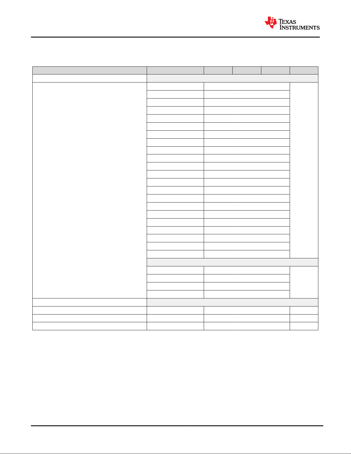
VIO
ZigBee
COEX
PM
MAC/PHY
32.768 kHz
WLAN_SDIO
BT_UART
WRF1
BTRF
BG2
BT
BG1
MAC/PHY
BT_EN
WLAN_EN
VBAT
RF_ANT1
RF_ANT2
26M XTAL
2.4-GHz
SPDT
WRF2
F
F
Interface
Copyright © 2017, Texas Instruments Incorporated
WL1801MOD, WL1805MOD, WL1831MOD, WL1835MOD
SWRS152N – JUNE 2013 – REVISED APRIL 2021
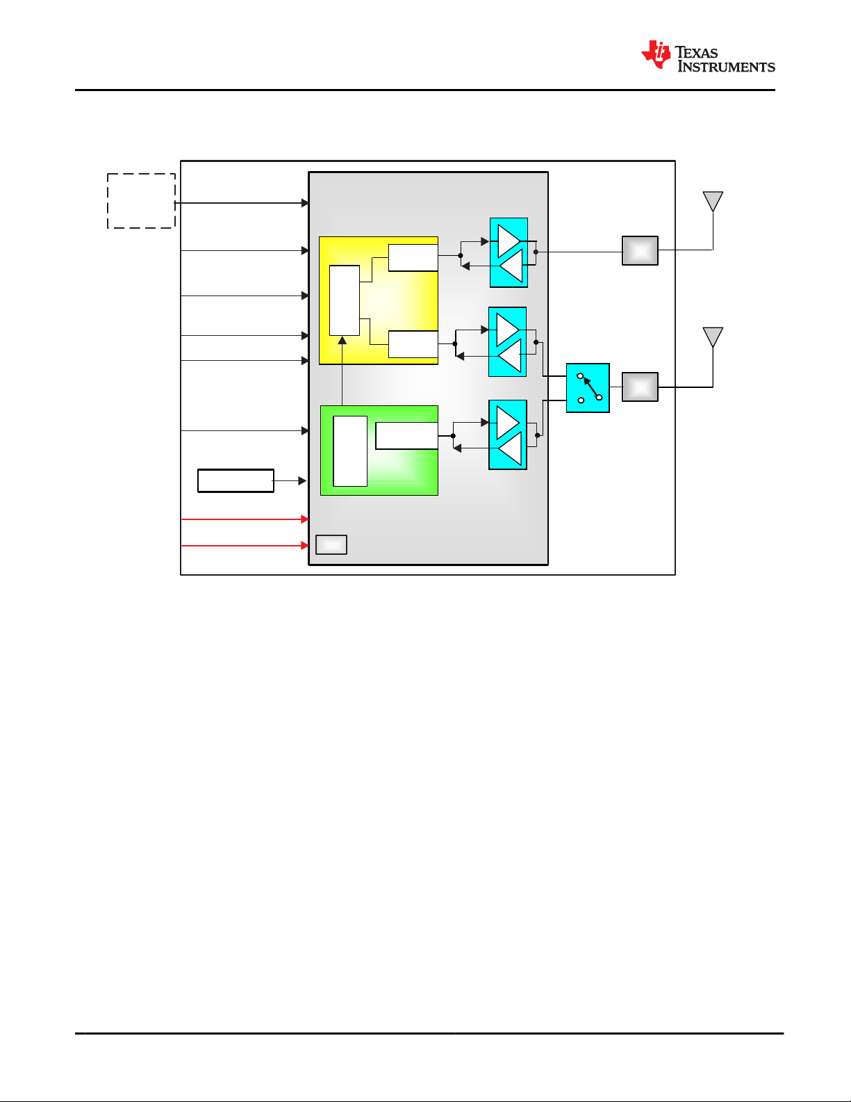
4 Functional Block Diagram
Figure 4-1 shows a functional block diagram of the WL1835MOD variant.
www.ti.com
NOTE: Dashed lines indicate optional configurations and are not applied by default.
Figure 4-1. WL1835MOD Functional Block Diagram
2 Submit Document Feedback
Product Folder Links: WL1801MOD WL1805MOD WL1831MOD WL1835MOD
Copyright © 2021 Texas Instruments Incorporated

www.ti.com
WL1801MOD, WL1805MOD, WL1831MOD, WL1835MOD
SWRS152N – JUNE 2013 – REVISED APRIL 2021
Table of Contents
1 Features............................................................................1
2 Applications..................................................................... 1
3 Description.......................................................................1
4 Functional Block Diagram.............................................. 2
5 Revision History.............................................................. 3
6 Device Comparison......................................................... 4
6.1 Related Products........................................................ 4
7 Terminal Configuration and Functions..........................5
7.1 Pin Attributes...............................................................6
8 Specifications.................................................................. 9
8.1 Absolute Maximum Ratings........................................ 9
8.2 ESD Ratings............................................................... 9
8.3 Recommended Operating Conditions.........................9
8.4 External Digital Slow Clock Requirements................10
8.5 Thermal Resistance Characteristics for MOC
100-Pin Package......................................................... 10
8.6 WLAN Performance: 2.4-GHz Receiver
Characteristics.............................................................11
8.7 WLAN Performance: 2.4-GHz Transmitter Power.... 12
8.8 WLAN Performance: Currents.................................. 13
8.9 Bluetooth Performance: BR, EDR Receiver
Characteristics—In-Band Signals................................13
8.10 Bluetooth Performance: Transmitter, BR ............... 15
8.11 Bluetooth Performance: Transmitter, EDR..............15
8.12 Bluetooth Performance: Modulation, BR.................15
8.13 Bluetooth Performance: Modulation, EDR.............. 16
8.14 Bluetooth low energy Performance: Receiver
Characteristics – In-Band Signals............................... 16
8.15 Bluetooth low energy Performance: Transmitter
Characteristics.............................................................16
8.16 Bluetooth low energy Performance: Modulation
Characteristics.............................................................17
8.17 Bluetooth BR and EDR Dynamic Currents............. 17
8.18 Bluetooth low energy Currents................................17
8.19 Timing and Switching Characteristics..................... 18
9 Detailed Description......................................................26
9.1 WLAN Features........................................................ 27
9.2 Bluetooth Features....................................................27
9.3 Bluetooth Low Energy Features................................28
9.4 Device Certification................................................... 28
9.5 Module Markings.......................................................30
9.6 Test Grades...............................................................30
9.7 End Product Labeling................................................31
9.8 Manual Information to the End User......................... 31
10 Applications, Implementation, and Layout............... 32
10.1 Application Information........................................... 32
11 Device and Documentation Support..........................38
11.1 Device Support........................................................38
11.2 Support Resources................................................. 41
11.3 Trademarks............................................................. 41
11.4 Electrostatic Discharge Caution..............................41
11.5 Glossary..................................................................41
12 Mechanical, Packaging, and Orderable
Information.................................................................... 42
12.1 TI Module Mechanical Outline................................ 42
12.2 Tape and Reel Information......................................42
12.3 Packaging Information............................................ 45
5 Revision History
NOTE: Page numbers for previous revisions may differ from page numbers in the current version.
Changes from November 1, 2017 to April 26, 2021 Page
• Updated the numbering format for tables, figures and cross-references throughout the document...................1
• Updated to "Bluetooth 5.1 Secure Connection..." in Section 1 .......................................................................... 1
• Updated Section 6.1, Related Products .............................................................................................................4
• Updated "Bluetooth 4.2" to "Bluetooth 5.1" in Section 9.2 ...............................................................................27
• Updated "Bluetooth 4.2" to "Bluetooth 5.1" in Section 9.3 ...............................................................................28
• Deleted the sentence that began "Moreover, the module is also Wi-Fi certified..." in the first paragraph in
Section 9.4, Device Certification ......................................................................................................................28
Copyright © 2021 Texas Instruments Incorporated
Product Folder Links: WL1801MOD WL1805MOD WL1831MOD WL1835MOD
Submit Document Feedback
3
WL1801MOD, WL1805MOD, WL1831MOD, WL1835MOD
SWRS152N – JUNE 2013 – REVISED APRIL 2021
www.ti.com
6 Device Comparison
The TI WiLink 8 module offers four footprint-compatible 2.4-GHz variants providing stand-alone Wi-Fi and
Bluetooth combo connectivity. Table 6-1 compares the features of the module variants.
Table 6-1. TI WiLink™ 8 Module Variants
FEATURE
WLAN 2.4-GHz SISO
WLAN 2.4-GHz MIMO
WLAN 2.4-GHz MRC
Bluetooth ✓ ✓
(1) SISO: single input, single output; MIMO: multiple input, multiple output; MRC: maximum ratio combining, supported at 802.11 g/n.
(1)
(1)
(1)
WL1835MOD WL1831MOD WL1805MOD WL1801MOD
✓ ✓ ✓ ✓
✓ ✓
✓ ✓
6.1 Related Products
For information about other devices in this family of products or related products, see the following links.
Wireless connectivity overview Lowest power and longest range across 14 wireless connectivity
standards
Sub-1 GHz SimpleLink™ wireless
MCUs
Reference Designs for WL1835MOD Find reference designs leveraging the best in TI technology to solve
High performance, long range wireless and ultra-low power
consumption
your system-level challenges
DEVICE
4 Submit Document Feedback
Product Folder Links: WL1801MOD WL1805MOD WL1831MOD WL1835MOD
Copyright © 2021 Texas Instruments Incorporated

PIN 19 - GND
PIN 17 - GND
PIN 20 - GND
PIN 23 - GND
PIN 24 - GND
PIN 28 - GND
PIN 29 - GND
PIN 30 - GND
PIN 31 - GND
PIN 18 - RF_ANT2
PIN 21 - RESERVED1
PIN 22 - RESERVED2
PIN 25 - GPIO4
PIN 26 - GPIO2
PIN 27 - GPIO1
PIN 32 - RF_ANT1
PIN 1 - GND
PIN 4 - GPIO10
PIN 5 - GPIO12
PIN 2 - GPIO11
PIN 3 - GPIO9
PIN 6 - WL_SDIO_CMD
PIN 8 - WL_SDIO_CLK
PIN 7 - GND
PIN 9 - GND
PIN 10 - WL_SDIO_D0
PIN 11 - WL_SDIO_D1
PIN 12 - WL_SDIO_D2
PIN 13 - WL_SDIO_D3
PIN 14 - WLAN_IRQ
PIN 15 - GND
PIN 16 - GND
PIN 33 - GND
PIN 40 - WLAN_EN
PIN 38 - VIO
PIN 39 - GND
PIN 37 - GND
PIN 41 - BT_EN
PIN 43 - BT_UART_DBG
PIN 46 - VBAT_IN
PIN 36 - EXT_32K
PIN 34 - GND
PIN 35 - GND
PIN 42 - WL_UART_DBG
PIN 44 - GND
PIN 45 - GND
PIN 47 - VBAT_IN
PIN 48 - GND
PIN 49 - GND
PIN 50 - BT_HCI_RTS
PIN 51 - BT_HCI_CTS
PIN 52 - BT_HCI_TX
PIN 53 - BT_HCI_RX
PIN 54 - GND
PIN 55 - GND
PIN 56 - BT_AUD_IN
PIN 57 - BT_AUD_OUT
PIN 58 - BT_AUD_FSYNC
PIN 60 - BT_AUD_CLK
PIN 59 - GND
PIN 61 - GND
PIN 63 - GND
PIN 62 - RESERVED3
PIN 64 - GND
GND
GND
GND
GND
GND
GND
GND
GND
GND
GND
GND
GND
GND
GND
GND
GND
GND
GND
GND
GND
GND
GND
GND
GND
GND
GND
GND
GND
GND
GND
GND
GND
GND
GND
GND
GND
Pin 2 Indicator
www.ti.com
WL1801MOD, WL1805MOD, WL1831MOD, WL1835MOD
7 Terminal Configuration and Functions
Figure 7-1 shows the pin assignments for the 100-pin MOC package.
SWRS152N – JUNE 2013 – REVISED APRIL 2021
Figure 7-1. 100-Pin MOC Package (Bottom View)
Copyright © 2021 Texas Instruments Incorporated
Product Folder Links: WL1801MOD WL1805MOD WL1831MOD WL1835MOD
Submit Document Feedback
5
WL1801MOD, WL1805MOD, WL1831MOD, WL1835MOD
SWRS152N – JUNE 2013 – REVISED APRIL 2021
7.1 Pin Attributes
Table 7-1 describes the module pins.
www.ti.com
Table 7-1. Pin Attributes
(2)
DESCRIPTION
(3)
WLAN SDIO clock.
Must be driven by the
host.
Input sleep clock:
32.768 kHz
Mode setting: high =
enable
Mode setting: high =
enable
Connect to 1.8-V
external VIO
Power supply input, 2.9
to 4.8 V
Power supply input, 2.9
to 4.8 V
Reserved for future
use. NC if not used.
Reserved for future
use. NC if not used.
Reserved for future
use. NC if not used.
Reserved for future
use. NC if not used.
Reserved for future
use. NC if not used.
Reserved for future
use. NC if not used.
Reserved for future
use. NC if not used.
Reserved for future
use. NC if not used.
WLAN SDIO data bit
3. Changes state to
PU at WL_EN or
BT_EN assertion for
card detects. Later
disabled by software
during initialization.
PIN NAME
PIN
NO.
TYPE/
DIR
SHUTDOWN
STATE
(1)
AFTER
POWER
(1)
UP
VOLTAGE
LEVEL
CONNECTIVITY
1801 1805 1831 1835
Clocks and Reset Signals
WL_SDIO_CLK 8 I Hi-Z Hi-Z 1.8 V v v v v
EXT_32K 36 ANA – v v v v
WLAN_EN 40 I PD PD 1.8 V v v v v
BT_EN 41 I PD PD 1.8 V x x v v
Power-Management Signals
VIO_IN 38 POW PD PD 1.8 V v v v v
VBAT_IN 46 POW VBAT v v v v
VBAT_IN 47 POW VBAT v v v v
TI Reserved
GPIO11 2 I/O PD PD 1.8 V v v v v
GPIO9 3 I/O PD PD 1.8 V v v v v
GPIO10 4 I/O PU PU 1.8 V v v v v
GPIO12 5 I/O PU PU 1.8 V v v v v
RESERVED1 21 I PD PD 1.8 V x x x x
RESERVED2 22 I PD PD 1.8 V x x x x
GPIO4 25 I/O PD PD 1.8 V v v v v
RESERVED3 62 O PD PD 1.8 V x x x x
WLAN Functional Block: Int Signals
WL_SDIO_CMD_1V8 6 I/O Hi-Z Hi-Z 1.8 V v v v v WLAN SDIO command
WL_SDIO_D0_1V8 10 I/O Hi-Z Hi-Z 1.8 V v v v v WLAN SDIO data bit 0
WL_SDIO_D1_1V8 11 I/O Hi-Z Hi-Z 1.8 V v v v v WLAN SDIO data bit 1
WL_SDIO_D2_1V8 12 I/O Hi-Z Hi-Z 1.8 V v v v v WLAN SDIO data bit 2
WL_SDIO_D3_1V8 13 I/O Hi-Z PU 1.8 V v v v v
6 Submit Document Feedback
Product Folder Links: WL1801MOD WL1805MOD WL1831MOD WL1835MOD
Copyright © 2021 Texas Instruments Incorporated

www.ti.com
WL1801MOD, WL1805MOD, WL1831MOD, WL1835MOD
SWRS152N – JUNE 2013 – REVISED APRIL 2021
Table 7-1. Pin Attributes (continued)
(2)
DESCRIPTION
(3)
WLAN SDIO out-ofband interrupt line.
Set to rising edge
(active high) by
default. (To extract
the debug option
WL_RS232_TX/RX
interface out, pull up
the IRQ line at power
up before applying
enable.)
2.4-GHz ANT2 TX, RX;
2.4-GHz secondary
antenna MRC/MIMO
only.
WL_RS232_RX (when
WLAN_IRQ = 1 at
power up)
WL_RS232_TX (when
WLAN_IRQ = 1 at
power up)
2.4-GHz WLAN
main antenna SISO,
Bluetooth
Option: Bluetooth
logger
UART RTS to host. NC
if not used.
UART CTS from host.
NC if not used.
UART TX to host. NC if
not used.
UART RX from host.
NC if not used.
Bluetooth PCM/I2S
bus. Data in. NC if not
used.
Bluetooth PCM/I2S
bus. Data out. NC if not
used.
Bluetooth PCM/I2S
bus. Frame sync. NC if
not used.
Bluetooth PCM/I2S
bus. NC if not used.
PIN NAME
PIN
NO.
TYPE/
DIR
SHUTDOWN
STATE
(1)
AFTER
POWER
(1)
UP
VOLTAGE
LEVEL
CONNECTIVITY
1801 1805 1831 1835
WL_IRQ_1V8 14 O PD 0 1.8 V v v v v
RF_ANT2
18 ANA – x v x v
GPIO2 26 I/O PD PD 1.8 V v v v v
GPIO1 27 I/O PD PD 1.8 V v v v v
RF_ANT1 32 ANA – v v v v
WL_UART_DBG 42 O PU PU 1.8 V v v v v Option: WLAN logger
Bluetooth Functional Block: Int Signals
BT_UART_DBG 43 O PU PU 1.8 V x x v v
BT_HCI_RTS_1V8 50 O PU PU 1.8 V x x v v
BT_HCI_CTS_1V8 51 I PU PU 1.8 V x x v v
BT_HCI_TX_1V8 52 O PU PU 1.8 V x x v v
BT_HCI_RX_1V8 53 I PU PU 1.8 V x x v v
BT_AUD_IN 56 I PD PD 1.8 V x x v v
BT_AUD_OUT 57 O PD PD 1.8 V x x v v
BT_AUD_FSYNC 58 I/O PD PD 1.8 V x x v v
BT_AUD_CLK 60 I/O PD PD 1.8 V x x v v
Copyright © 2021 Texas Instruments Incorporated
Product Folder Links: WL1801MOD WL1805MOD WL1831MOD WL1835MOD
Submit Document Feedback
7
WL1801MOD, WL1805MOD, WL1831MOD, WL1835MOD
SWRS152N – JUNE 2013 – REVISED APRIL 2021
www.ti.com
Table 7-1. Pin Attributes (continued)
(2)
PIN NAME
PIN
NO.
TYPE/
DIR
SHUTDOWN
STATE
(1)
AFTER
POWER
(1)
UP
VOLTAGE
LEVEL
CONNECTIVITY
1801 1805 1831 1835
Ground Pins
GND 1 GND – v v v v
GND 7 GND – v v v v
GND 9 GND – v v v v
GND 15 GND – v v v v
GND 16 GND – v v v v
GND 17 GND – v v v v
GND 19 GND – v v v v
GND 20 GND – v v v v
GND 23 GND – v v v v
GND 24 GND – v v v v
GND 28 GND – v v v v
GND 29 GND – v v v v
GND 30 GND – v v v v
GND 31 GND – v v v v
GND 33 GND – v v v v
GND 34 GND – v v v v
GND 35 GND – v v v v
GND 37 GND – v v v v
GND 39 GND – v v v v
GND 44 GND – v v v v
GND 45 GND – v v v v
GND 48 GND – v v v v
GND 49 GND – v v v v
GND 54 GND – v v v v
GND 55 GND – v v v v
GND 59 GND – v v v v
GND 61 GND – v v v v
GND 63 GND – v v v v
GND 64 GND – v v v v
GND
G1 –
GND – v v v v
G36
DESCRIPTION
(3)
(1) PU = pullup; PD = pulldown; Hi-Z = high-impedance
(2) v = connect; x = no connect
(3) Host must provide PU using a 10-kΩ resistor for all non-CLK SDIO signals.
8 Submit Document Feedback
Product Folder Links: WL1801MOD WL1805MOD WL1831MOD WL1835MOD
Copyright © 2021 Texas Instruments Incorporated
www.ti.com
SWRS152N – JUNE 2013 – REVISED APRIL 2021
8 Specifications
All specifications are measured at the module pins using the TI WL1835MODCOM8 evaluation board. All
WL1801MOD, WL1805MOD, WL1831MOD, WL1835MOD
measurements are performed with V
unless otherwise indicated.
For level-shifting I/Os with the TI WL18x5MOD, see the Level Shifting WL18xx I/Os application report.
8.1 Absolute Maximum Ratings
over operating free-air temperature range (unless otherwise noted)
V
BAT
V
IO
Input voltage to analog pins –0.5 2.1 V
Input voltage limits (CLK_IN) –0.5 VDD_IO V
Input voltage to all other pins –0.5 (VDD_IO + 0.5 V) V
Operating ambient temperature –20 70
Storage temperature, T
stg
= 3.7 V, VIO = 1.8 V, 25°C for typical values with matched RF antennas,
BAT
Note
(1)
MIN MAX UNIT
(2)
4.8
–0.5 2.1 V
(3)
–40 85 °C
V
°C
(1) Stresses beyond those listed under Absolute Maximum Ratings may cause permanent damage to the device. These are stress ratings
only and functional operation of the device at these or any other conditions beyond those indicated under Operating Conditions is not
implied. Exposure to absolute-maximum-rated conditions for extended periods may affect device reliability.
(2) 4.8 V cumulative to 2.33 years, including charging dips and peaks
(3) In the WL18xx system, a control mechanism exists to ensure Tj < 125°C. When Tj approaches this threshold, the control mechanism
manages the transmitter patterns.
8.2 ESD Ratings
VALUE
V
Electrostatic discharge
(ESD)
Human body model (HBM), per ANSI/ESDA/JEDEC JS-001
Charged device model (CDM), per JEDEC specification JESD22-C101
(1)
(2)
±1000
±250
(1) JEDEC document JEP155 states that 500-V HBM allows safe manufacturing with a standard ESD control process.
(2) JEDEC document JEP157 states that 250-V CDM allows safe manufacturing with a standard ESD control process.
UNIT
V
8.3 Recommended Operating Conditions
over operating free-air temperature range (unless otherwise noted)
MIN TYP MAX UNIT
(1)
V
BAT
V
IO
V
IH
V
IL
V
IH_EN
V
IL_EN
V
OH
V
OL
Tr,T
T
r
T
f
f
DC supply range for all modes 2.9 3.7 4.8 V
1.8-V I/O ring power supply voltage 1.62 1.8 1.95 V
I/O high-level input voltage 0.65 × VDD_IO VDD_IO V
I/O low-level input voltage 0 0.35 × VDD_IO V
Enable inputs high-level input voltage 1.365 VDD_IO V
Enable inputs low-level input voltage 0 0.4 V
High-level output voltage At 4 mA VDD_IO –0.45 VDD_IO V
Low-level output voltage At 4 mA 0 0.45 V
Input transitions time Tr,Tf from 10% to 90% (digital I/O)
Output rise time from 10% to 90% (digital pins)
Output fall time from 10% to 90% (digital pins)
(2)
(2)
(2)
1 10 ns
CL < 25 pF 5.3 ns
CL < 25 pF 4.9 ns
Ambient operating temperature –20 70 °C
Copyright © 2021 Texas Instruments Incorporated
Product Folder Links: WL1801MOD WL1805MOD WL1831MOD WL1835MOD
Submit Document Feedback
9
WL1801MOD, WL1805MOD, WL1831MOD, WL1835MOD
SWRS152N – JUNE 2013 – REVISED APRIL 2021
over operating free-air temperature range (unless otherwise noted)
Maximum
power
dissipation
WLAN operation 2.8 W
Bluetooth operation 0.2
www.ti.com
MIN TYP MAX UNIT
(1) 4.8 V is applicable only for 2.33 years (30% of the time). Otherwise, maximum V
must not exceed 4.3 V.
BAT
(2) Applies to all digital lines except PCM and slow clock lines.
8.4 External Digital Slow Clock Requirements
The supported digital slow clock is 32.768 kHz digital (square wave). All core functions share a single input.
CONDITION MIN TYP MAX UNIT
Input slow clock frequency 32768 Hz
Input slow clock accuracy (initial,
temperature, and aging)
Tr, T
Input transition time (10% to 90%) 200 ns
f
Frequency input duty cycle 15% 50% 85%
VIH, VILInput voltage limits
Input impedance 1 MΩ
Input capacitance 5 pF
WLAN, Bluetooth ±250 ppm
Square wave,
DC coupled
0.65 x VDD_IO VDD_IO V
0 0.35 x VDD_IO
8.5 Thermal Resistance Characteristics for MOC 100-Pin Package
THERMAL METRICS
θ
JA
θ
JB
θ
JC
(1)
Junction to free air
(3)
Junction to board 6.06
Junction to case
(4)
(°C/W)
16.6
5.13
peak
(2)
(1) For more information about traditional and new thermal metrics, see the Semiconductor and IC Package Thermal Metrics Application
Report.
(2) These values are based on a JEDEC-defined 2S2P system (with the exception of the Theta JC [R
] value, which is based on
θJC
a JEDEC-defined 1S0P system) and will change based on environment as well as application. For more information, see these
EIA/JEDEC standards:
• JESD51-2, Integrated Circuits Thermal Test Method Environmental Conditions - Natural Convection (Still Air)
• JESD51-3, Low Effective Thermal Conductivity Test Board for Leaded Surface Mount Packages
• JESD51-7, High Effective Thermal Conductivity Test Board for Leaded Surface Mount Packages
• JESD51-9, Test Boards for Area Array Surface Mount Package Thermal Measurements
Power dissipation of 2 W and an ambient temperature of 70°C is assumed.
(3) According to the JEDEC EIA/JESD 51 document
(4) Modeled using the JEDEC 2s2p thermal test board with 36 thermal vias
10 Submit Document Feedback
Product Folder Links: WL1801MOD WL1805MOD WL1831MOD WL1835MOD
Copyright © 2021 Texas Instruments Incorporated
www.ti.com
SWRS152N – JUNE 2013 – REVISED APRIL 2021
8.6 WLAN Performance: 2.4-GHz Receiver Characteristics
over operating free-air temperature range (unless otherwise noted). All RF and performance numbers are aligned to the
module pin.
PARAMETER CONDITION MIN TYP MAX UNIT
RF_ANT1 pin 2.4-GHz SISO
Operation frequency range 2412 2484 MHz
1 Mbps DSSS –96.3
2 Mbps DSSS –93.2
5.5 Mbps CCK –90.6
11 Mbps CCK –87.9
6 Mbps OFDM –92.0
9 Mbps OFDM –90.4
12 Mbps OFDM –89.5
18 Mbps OFDM –87.2
24 Mbps OFDM –84.1
36 Mbps OFDM –80.7
48 Mbps OFDM –76.5
54 Mbps OFDM –74.9
MCS0 MM 4K –90.4
WL1801MOD, WL1805MOD, WL1831MOD, WL1835MOD
Sensitivity: 20-MHz bandwidth. At < 10% PER limit
Maximum input level
Adjacent channel rejection: Sensitivity level +3 dB for
OFDM; Sensitivity level +6 dB for 11b
MCS1 MM 4K –87.6
MCS2 MM 4K –85.9
MCS3 MM 4K –82.8
MCS4 MM 4K –79.4
MCS5 MM 4K –75.2
MCS6 MM 4K –73.5
MCS7 MM 4K –72.4
MCS0 MM 4K 40 MHz –86.7
MCS7 MM 4K 40 MHz –67.0
MCS0 MM 4K MRC –92.7
MCS7 MM 4K MRC –75.2
MCS13 MM 4K –73.7
MCS14 MM 4K –72.3
MCS15 MM 4K –71.0
OFDM –20.0 –10.0
DSSS –4.0 –1.0
2 Mbps DSSS 42.0
54 Mbps OFDM 2.0
dBm
dBmCCK –10.0 –6.0
dB11 Mbps CCK 38.0
Copyright © 2021 Texas Instruments Incorporated
Product Folder Links: WL1801MOD WL1805MOD WL1831MOD WL1835MOD
Submit Document Feedback
11
WL1801MOD, WL1805MOD, WL1831MOD, WL1835MOD
SWRS152N – JUNE 2013 – REVISED APRIL 2021
www.ti.com
8.7 WLAN Performance: 2.4-GHz Transmitter Power
over operating free-air temperature range (unless otherwise noted). All RF and performance numbers are aligned to the
module pin.
PARAMETER CONDITION
Output Power: Maximum RMS output power measured
at 1 dB from IEEE spectral mask or EVM
Operation frequency range 2412 2484 MHz
Return loss –10.0 dB
Reference input impedance 50.0 Ω
(2)
MCS0 MM 40 MHz 14.8
MCS7 MM 40 MHz 11.3
(1)
MIN TYP MAX UNIT
RF_ANT1 Pin 2.4-GHz SISO
1 Mbps DSSS 17.3
2 Mbps DSSS 17.3
5.5 Mbps CCK 17.3
11 Mbps CCK 17.3
6 Mbps OFDM 17.1
9 Mbps OFDM 17.1
12 Mbps OFDM 17.1
18 Mbps OFDM 17.1
24 Mbps OFDM 16.2
36 Mbps OFDM 15.3
48 Mbps OFDM 14.6
54 Mbps OFDM 13.8
MCS0 MM 16.1
MCS1 MM 16.1
MCS2 MM 16.1
MCS3 MM 16.1
MCS4 MM 15.3
MCS5 MM 14.6
MCS6 MM 13.8
MCS7 MM
(3)
12.6
RF_ANT1 + RF_ANT2
MCS12 (WL18x5) 18.5
MCS13 (WL18x5) 17.4
MCS14 (WL18x5) 14.5
MCS15 (WL18x5) 13.4
RF_ANT1 + RF_ANT2
dBm
dBm
(1) Maximum transmitter power (TP) degradation of up to 30% is expected, starting from 80°C ambient temperature on MIMO operation
(2) Regulatory constraints limit TI module output power to the following:
• Channel 14 is used only in Japan; to keep the channel spectral shaping requirement, the power is limited: 14.5 dBm.
• Channels 1, 11 at OFDM legacy and HT 20-MHz rates: 12 dBm
• Channels 1, 11 at HT 40-MHz rates: 10 dBm
• Channel 7 at HT 40-MHz lower rates: 10 dBm
• Channel 5 at HT 40-MHz upper rates: 10 dBm
• All 11B rates are limited to 16 dBm to comply with the ETSI PSD 10 dBm/MHz limit.
• All OFDM rates are limited to 16.5 dBm to comply with the ETSI EIRP 20 dBm limit.
• For clarification regarding power limitation, see the WL18xx .INI File Application Report.
(3) To ensure compliance with the EVM conditions specified in the PHY chapter of IEEE Std 802.11™ – 2012:
• MCS7 20 MHz channel 12 output power is 2 dB lower than the typical value.
12 Submit Document Feedback
Copyright © 2021 Texas Instruments Incorporated
Product Folder Links: WL1801MOD WL1805MOD WL1831MOD WL1835MOD
www.ti.com
• MCS7 20 MHz channel 8 output power is 1 dB lower than the typical value.
SWRS152N – JUNE 2013 – REVISED APRIL 2021
8.8 WLAN Performance: Currents
over operating free-air temperature range (unless otherwise noted). All RF and performance numbers are aligned to the
module pin.
PARAMETER SPECIFICATION TYP (AVG) –25°C UNIT
Low-power mode (LPM) 2.4-GHz RX SISO20 single chain 49
2.4 GHz RX search SISO20 54
2.4-GHz RX search MIMO20 74
2.4-GHz RX search SISO40 59
2.4-GHz RX 20 M SISO 11 CCK 56
WL1801MOD, WL1805MOD, WL1831MOD, WL1835MOD
Receiver
Transmitter
2.4-GHz RX 20 M SISO 6 OFDM 61
2.4-GHz RX 20 M SISO MCS7 65
2.4-GHz RX 20 M MRC 1 DSSS 74
2.4-GHz RX 20 M MRC 6 OFDM 81
2.4-GHz RX 20 M MRC 54 OFDM 85
2.4-GHz RX 40-MHz MCS7 77
2.4-GHz TX 20 M SISO 6 OFDM 15.4 dBm 285
2.4-GHz TX 20 M SISO 11 CCK 15.4 dBm 273
2.4-GHz TX 20 M SISO 54 OFDM 12.7 dBm 247
2.4-GHz TX 20 M SISO MCS7 11.2 dBm 238
2.4-GHz TX 20 M MIMO MCS15 11.2 dBm 420
2.4-GHz TX 40 M SISO MCS7 8.2 dBm 243
mA
mA
8.9 Bluetooth Performance: BR, EDR Receiver Characteristics—In-Band Signals
over operating free-air temperature range (unless otherwise noted)
PARAMETER
Bluetooth BR, EDR operation
frequency range
Bluetooth BR, EDR channel
spacing
Bluetooth BR, EDR input
impedance
Bluetooth BR, EDR
sensitivity
Dirty TX on
Bluetooth EDR BER floor at
sensitivity + 10 dB
Dirty TX off (for 1,600,000
bits)
Bluetooth BR, EDR maximum
usable input power
Bluetooth BR intermodulation Level of interferers for n = 3, 4, and 5 –36.0 –30.0 dBm
(2)
(1) (2)
CONDITION MIN TYP MAX UNIT
2402 2480 MHz
50 Ω
BR, BER = 0.1% –92.2
EDR2, BER = 0.01% –91.7
EDR3, BER = 0.01% –84.7
EDR2 1e-6
EDR3 1e-6
BR, BER = 0.1% –5.0
EDR3, BER = 0.1% –15.0
1 MHz
dBm
dBmEDR2, BER = 0.1% –15.0
Copyright © 2021 Texas Instruments Incorporated
Product Folder Links: WL1801MOD WL1805MOD WL1831MOD WL1835MOD
Submit Document Feedback
13
WL1801MOD, WL1805MOD, WL1831MOD, WL1835MOD
SWRS152N – JUNE 2013 – REVISED APRIL 2021
www.ti.com
over operating free-air temperature range (unless otherwise noted)
PARAMETER
Bluetooth BR, EDR C/I
performance
Numbers show wanted
signal-to-interfering-signal
ratio. Smaller numbers
indicate better C/I
performances (Image
frequency = –1 MHz)
Bluetooth BR, EDR RF return
loss
(1) All RF and performance numbers are aligned to the module pin.
(2) Sensitivity degradation up to –3 dB may occur due to fast clock harmonics with dirty TX on.
(1) (2)
CONDITION MIN TYP MAX UNIT
BR, co-channel 10
EDR, co-channel EDR2 12
EDR3 20
BR, adjacent ±1 MHz –3.0
EDR, adjacent ±1 MHz,
(image)
EDR2 –3.0
EDR3 2.0
BR, adjacent +2 MHz –33.0
EDR, adjacent +2 MHz EDR2 –33.0
EDR3 –28.0
BR, adjacent –2 MHz –20.0
EDR, adjacent –2 MHz EDR2 –20.0
EDR3 –13.0
BR, adjacent ≥Ι±3Ι MHz –42.0
EDR, adjacent ≥Ι±3Ι MHz EDR2 –42.0
EDR3 –36.0
dB
–10.0 dB
14 Submit Document Feedback
Product Folder Links: WL1801MOD WL1805MOD WL1831MOD WL1835MOD
Copyright © 2021 Texas Instruments Incorporated
www.ti.com
8.10 Bluetooth Performance: Transmitter, BR
WL1801MOD, WL1805MOD, WL1831MOD, WL1835MOD
SWRS152N – JUNE 2013 – REVISED APRIL 2021
over operating free-air temperature range (unless otherwise noted)
PARAMETER
BR RF output power
(2)
BR gain control range 30.0 dB
BR power control step 5.0 dB
BR adjacent channel power |M-N| = 2 –43.0 dBm
BR adjacent channel power |M-N| > 2 –48.0 dBm
(1) All RF and performance numbers are aligned to the module pin.
(2) Values reflect maximum power. Reduced power is available using a vendor-specific (VS) command.
(3) VBAT is measured with an on-chip ADC that has an accuracy error of up to 5%.
(1)
≥ 3 V
< 3 V
(3)
(3)
V
BAT
V
BAT
MIN TYP MAX UNIT
11.7
7.2
dBm
8.11 Bluetooth Performance: Transmitter, EDR
over operating free-air temperature range (unless otherwise noted)
PARAMETER
EDR output power
EDR gain control range 30 dB
EDR power control step 5 dB
EDR adjacent channel power |M-N| = 1 –36 dBc
EDR adjacent channel power |M-N| = 2 –30 dBm
EDR adjacent channel power |M-N| > 2 –42 dBm
(2)
(1)
≥ 3 V
< 3 V
(3)
(3)
V
BAT
V
BAT
MIN TYP MAX UNIT
7.2
5.2
dBm
(1) All RF and performance numbers are aligned to the module pin.
(2) Values reflect default maximum power. Maximum power can be changed using a VS command.
(3) VBAT is measured with an on-chip ADC that has an accuracy error of up to 5%.
8.12 Bluetooth Performance: Modulation, BR
over operating free-air temperature range (unless otherwise noted)
CHARACTERISTICS
BR –20-dB bandwidth 925 995 kHz
BR modulation characteristics
BR carrier frequency drift One-slot packet –25 25 kHz
BR drift rate lfk+5 – fkl , k = 0 to max 15 kHz/50 µs
BR initial carrier frequency tolerance
(1) All RF and performance numbers are aligned to the module pin.
(2) Performance values reflect maximum power.
(3) Numbers include XTAL frequency drift over temperature and aging.
(1)
CONDITION
∆f1avg Mod data = 4 1s, 4 0s:
(2)
MIN TYP MAX UNIT
145 160 170 kHz
111100001111...
∆f2max ≥ limit for
Mod data = 1010101... 120 130 kHz
at least 99.9% of all
Δf2max
∆f2avg, ∆f1avg 85% 88%
Three- and five-slot
–35 35 kHz
packet
(3)
f0–fTX ±75 ±75 kHz
Copyright © 2021 Texas Instruments Incorporated
Product Folder Links: WL1801MOD WL1805MOD WL1831MOD WL1835MOD
Submit Document Feedback
15

WL1801MOD, WL1805MOD, WL1831MOD, WL1835MOD
SWRS152N – JUNE 2013 – REVISED APRIL 2021
8.13 Bluetooth Performance: Modulation, EDR
www.ti.com
over operating free-air temperature range (unless otherwise noted)
PARAMETER
EDR carrier frequency stability –5 5 kHz
EDR initial carrier frequency tolerance
EDR RMS DEVM
EDR 99% DEVM
EDR peak DEVM
(1) All RF and performance numbers are aligned to the module pin.
(2) Performance values reflect maximum power.
(3) Numbers include XTAL frequency drift over temperature and aging.
(1) (2)
CONDITION MIN TYP MAX UNIT
(3)
±75 ±75 kHz
EDR2 4% 15%
EDR3 4% 10%
EDR2 30%
EDR3 20%
EDR2 9% 25%
EDR3 9% 18%
8.14 Bluetooth low energy Performance: Receiver Characteristics – In-Band Signals
over operating free-air temperature range (unless otherwise noted)
PARAMETER
Bluetooth low energy operation frequency range 2402 2480 MHz
Bluetooth low energy channel spacing 2 MHz
Bluetooth low energy input impedance 50 Ω
Bluetooth low energy sensitivity
Dirty TX on
Bluetooth low energy maximum usable input power –5 dBm
Bluetooth low energy intermodulation
characteristics
Bluetooth low energy C/I performance.
Note: Numbers show wanted signal-to-interferingsignal ratio. Smaller numbers indicate better C/I
performance.
Image = –1 MHz
(1)
(3)
CONDITION
Level of interferers.
For n = 3, 4, 5
(2)
MIN TYP MAX UNIT
–92.2
–36 –30
dBm
dBm
Low energy, co-channel 12
Low energy, adjacent ±1 MHz 0
Low energy, adjacent +2 MHz –38
dB
Low energy, adjacent –2 MHz –15
Low energy, adjacent ≥ |±3| MHz –40
(1) All RF and performance numbers are aligned to the module pin.
(2) BER of 0.1% corresponds to PER of 30.8% for a minimum of 1500 transmitted packets, according to the Bluetooth low energy test
specification.
(3) Sensitivity degradation of up to –3 dB can occur due to fast clock harmonics.
8.15 Bluetooth low energy Performance: Transmitter Characteristics
over operating free-air temperature range (unless otherwise noted)
PARAMETER
Bluetooth low energy RF output power
Bluetooth low energy adjacent channel power |M-N| = 2 –51.0 dBm
Bluetooth low energy adjacent channel power |M-N| > 2 –54.0 dBm
(1) All RF and performance numbers are aligned to the module pin.
(2) Bluetooth low energy power is restricted to comply with the ETSI 10-dBm EIRP limit requirement.
(3) VBAT is measured with an on-chip ADC that has an accuracy error of up to 5%.
16 Submit Document Feedback
(1)
≥ 3 V
< 3 V
(3)
(3)
V
(2)
BAT
V
BAT
MIN TYP MAX UNIT
7.0
7.0
Copyright © 2021 Texas Instruments Incorporated
Product Folder Links: WL1801MOD WL1805MOD WL1831MOD WL1835MOD
dBm

www.ti.com
WL1801MOD, WL1805MOD, WL1831MOD, WL1835MOD
8.16 Bluetooth low energy Performance: Modulation Characteristics
SWRS152N – JUNE 2013 – REVISED APRIL 2021
over operating free-air temperature range (unless otherwise noted)
CHARACTERISTICS
(1)
CONDITION
∆f1avg Mod data = 4 1s, 4 0s:
Bluetooth low energy
modulation characteristics
∆f2max ≥ limit for
at least 99.9% of all
Δf2max
∆f2avg, ∆f1avg 85% 90%
Bluetooth low energy carrier
frequency drift
lf0 – fnl , n = 2,3 …. K –25 25 kHz
Bluetooth low energy drift rate lf1 – f0l and lfn – fn-5l , n = 6,7…. K 15 kHz/50 µs
Bluetooth low energy initial
carrier frequency tolerance
fn – fTX ±75 ±75 kHz
(3)
(1) All RF and performance numbers are aligned to the module pin.
(2) Performance values reflect maximum power.
(3) Numbers include XTAL frequency drift over temperature and aging.
(2)
111100001111...
Mod data = 1010101...
MIN TYP MAX UNIT
240 250 260
kHz
195 215
8.17 Bluetooth BR and EDR Dynamic Currents
Current is measured at output power as follows: BR at 11.7 dBm; EDR at 7.2 dBm.
USE CASE
BR voice HV3 + sniff 11.6 mA
EDR voice 2-EV3 no retransmission + sniff 5.9 mA
Sniff 1 attempt 1.28 s 178.0 µA
EDR A2DP EDR2 (master). SBC high quality – 345 kbps 10.4 mA
EDR A2DP EDR2 (master). MP3 high quality – 192 kbps 7.5 mA
Full throughput ACL RX: RX-2DH5
Full throughput BR ACL TX: TX-DH5
Full throughput EDR ACL TX: TX-2DH5
Page scan or inquiry scan (scan interval is 1.28 s or 11.25 ms, respectively) 253.0 µA
Page scan and inquiry scan (scan interval is 1.28 s and 2.56 s, respectively) 332.0 µA
(3) (4)
(4)
(4)
(1) (2)
TYP UNIT
18.0 mA
50.0 mA
33.0 mA
(1) The role of Bluetooth in all scenarios except A2DP is slave.
(2) CL1P5 PA is connected to V
BAT
, 3.7 V.
(3) ACL RX has the same current in all modulations.
(4) Full throughput assumes data transfer in one direction.
8.18 Bluetooth low energy Currents
All current measured at output power of 7.0 dBm
USE CASE
Advertising, not connectable
Advertising, discoverable
Scanning
(3)
Connected, master role, 1.28-s connect interval
Connected, slave role, 1.28-s connect interval
(1) CL1p% PA is connected to V
(2) Advertising in all three channels, 1.28-s advertising interval, 15 bytes advertise data
(3) Listening to a single frequency per window, 1.28-s scan interval, 11.25-ms scan window
(4) Zero slave connection latency, empty TX and RX LL packets
Copyright © 2021 Texas Instruments Incorporated
(2)
(2)
(4)
(4)
, 3.7 V.
BAT
Product Folder Links: WL1801MOD WL1805MOD WL1831MOD WL1835MOD
(1)
TYP UNIT
131 µA
143 µA
266 µA
124 µA
132 µA
Submit Document Feedback
17

WL18xx Top Level
Main DC2DC
V
BAT
VIO
FB
SW
PA
DC2DC
FB
SW
Digital DC2DC
FB
SW
1.8 V
2.2 – 2.7 V
VBAT
VIO_IN
VBAT_IN_MAIN_DC2DC
VBAT_IN_PA_DC2DC
VBAT
MAIN_DC2DC_OUT
DIG_DC2DC_OUT
VDD_DIG
LDO_IN_DIG
PA_DC2DC_OUT
FB_IN_PA_DC2DC
1 V
>10 µs
1
2
3
>10 µs
4
5 5
>
60 µs
VBAT
VIO
EXT_32K
WLEN
WL1801MOD, WL1805MOD, WL1831MOD, WL1835MOD
SWRS152N – JUNE 2013 – REVISED APRIL 2021
www.ti.com
8.19 Timing and Switching Characteristics
8.19.1 Power Management
8.19.1.1 Block Diagram – Internal DC-DCs
The device incorporates three internal DC-DCs (switched-mode power supplies) to provide efficient internal
supplies, derived from V
8.19.2 Power-Up and Shut-Down States
BAT
.
Figure 8-1. Internal DC-DCs
The correct power-up and shut-down sequences must be followed to avoid damage to the device.
While V
or VIO or both are deasserted, no signals should be driven to the device. The only exception is the
BAT
slow clock that is a fail-safe I/O.
While V
, VIO, and slow clock are fed to the device, but WL_EN is deasserted (low), the device is in
BAT
SHUTDOWN state. In SHUTDOWN state all functional blocks, internal DC-DCs, clocks, and LDOs are disabled.
To perform the correct power-up sequence, assert (high) WL_EN. The internal DC-DCs, LDOs, and clock start
to ramp and stabilize. Stable slow clock, VIO, and V
are prerequisites to the assertion of one of the enable
BAT
signals.
To perform the correct shut-down sequence, deassert (low) WL_EN while all the supplies to the device (V
VIO, and slow clock) are still stable and available. The supplies to the chip (V
and VIO) can be deasserted only
BAT
BAT
after both enable signals are deasserted (low).
Figure 8-2 shows the general power scheme for the module, including the power-down sequence.
,
NOTE: 1. Either VBAT or VIO can come up first.
NOTE: 2. VBAT and VIO supplies and slow clock (SCLK), must be stable prior to EN being asserted and at all times
NOTE: when the EN is active.
NOTE: 3. At least 60 µs is required between two successive device enables. The device is assumed to be in
NOTE: shutdown state during that period, meaning all enables to the device are LOW for that minimum duration.
18 Submit Document Feedback
Product Folder Links: WL1801MOD WL1805MOD WL1831MOD WL1835MOD
Copyright © 2021 Texas Instruments Incorporated

VBAT / VIO
input
EXT_32K
input
WL_EN
input
Main 1V8 DC2DC
TCXO_CLK_REQ
output
DIG DC2DC
SRAM LDO
Internal power stable = 5 ms
Top RESETZ
4.5 ms delay
www.ti.com
NOTE: 4. EN must be deasserted at least 10 µs before VBAT or VIO supply can be lowered (order of supply turn off
NOTE: after EN shutdown is immaterial).
NOTE: 5. EXT_32K - Fail safe I/O
SWRS152N – JUNE 2013 – REVISED APRIL 2021
Figure 8-2. Power-Up System
8.19.3 Chip Top-level Power-Up Sequence
Figure 8-3 shows the top-level power-up sequence for the chip.
WL1801MOD, WL1805MOD, WL1831MOD, WL1835MOD
Figure 8-3. Chip Top-Level Power-Up Sequence
Copyright © 2021 Texas Instruments Incorporated
Product Folder Links: WL1801MOD WL1805MOD WL1831MOD WL1835MOD
Submit Document Feedback
19

Indicates completion of firmware download
and internal initialization
Wake-up time
SLOWCLK
input
WL_EN
input
SDIO_CLK
input
WLAN_IRQ
output
TCXO
input
TCXO_CLK_REQ
output
TXCO_LDO
output
VBAT / VIO
input
NLCP
WLAN_IRQ
output
MCP
Host configures device to
reverse WLAN_IRQ polarity
Wake-up time
Indicates completion of firmware download
and internal initialization
NLCP: trigger at rising edge
MCP: trigger at low level
Completion of Bluetooth firmware initialztion.
Initialization time
WL1801MOD, WL1805MOD, WL1831MOD, WL1835MOD
SWRS152N – JUNE 2013 – REVISED APRIL 2021
8.19.4 WLAN Power-Up Sequence
Figure 8-4 shows the WLAN power-up sequence.
www.ti.com
Figure 8-4. WLAN Power-Up Sequence
8.19.5 Bluetooth-Bluetooth low energy Power-Up Sequence
Figure 8-5 shows the Bluetooth-Bluetooth low energy power-up sequence.
Figure 8-5. Bluetooth-Bluetooth low energy Power-Up Sequence
20 Submit Document Feedback
Product Folder Links: WL1801MOD WL1805MOD WL1831MOD WL1835MOD
Copyright © 2021 Texas Instruments Incorporated

t
THL
t
TLH
V
IH
V
IL
V
IL
V
IH
V
IH
t
IH
t
ISU
V
IH
V
IH
Valid
V
IL
V
IL
V
DD
V
DD
V
SS
V
SS
NotValid
NotValid
ClockInput
DataInput
t
WL
t
WH
t
THL
t
TLH
V
IH
V
IL
V
IL
V
IH
V
IH
V
OH
Valid
V
OL
V
DD
V
DD
V
SS
V
SS
NotValidNotValid
ClockInput
DataOutput
t
WL
V
OH
V
OL
t
WH
t
ODLY(max)
t
ODLY(min)
www.ti.com
SWRS152N – JUNE 2013 – REVISED APRIL 2021
8.19.6 WLAN SDIO Transport Layer
The SDIO is the host interface for WLAN. The interface between the host and the WL18xx module uses an SDIO
interface and supports a maximum clock rate of 50 MHz.
The device SDIO also supports the following features of the SDIO V3 specification:
• 4-bit data bus
• Synchronous and asynchronous in-band interrupt
• Default and high-speed (HS, 50 MHz) timing
• Sleep and wake commands
8.19.6.1 SDIO Timing Specifications
Figure 8-6 and Figure 8-7 show the SDIO switching characteristics over recommended operating conditions and
with the default rate for input and output.
WL1801MOD, WL1805MOD, WL1831MOD, WL1835MOD
Figure 8-6. SDIO Default Input Timing
Figure 8-7. SDIO Default Output Timing
Table 8-1 lists the SDIO default timing characteristics.
Table 8-1. SDIO Default Timing Characteristics
(1)
f
clock
Clock frequency, CLK
DC Low, high duty cycle
t
TLH
t
THL
t
ISU
t
IH
t
ODLY
C
l
(1) To change the data out clock edge from the falling edge (default) to the rising edge, set the configuration bit.
(2) Parameter values reflect maximum clock frequency.
Copyright © 2021 Texas Instruments Incorporated
Rise time, CLK
Fall time, CLK
Setup time, input valid before CLK ↑
Hold time, input valid after CLK ↑
Delay time, CLK ↓ to output valid
Capacitive load on outputs
(2)
(2)
(2)
(2)
(2)
(2)
(2)
(2)
Product Folder Links: WL1801MOD WL1805MOD WL1831MOD WL1835MOD
MIN MAX UNIT
0.0 26.0 MHz
40.0% 60.0%
10.0 ns
10.0 ns
3.0 ns
2.0 ns
7.0 10.0 ns
15.0 pF
Submit Document Feedback
21

t
THL
t
TLH
V
IH
V
IL
V
IL
V
IH
V
IH
V
IH
V
IH
Valid
V
IL
V
IL
V
DD
V
DD
V
SS
V
SS
NotValid
NotValid
ClockInput
DataInput
t
WL
t
WH
t
ISU
t
IH
50%V
DD
t
THL
t
TLH
V
IH
V
IL
V
IH
V
IH
V
OH
Valid
V
OL
V
DD
V
DD
V
SS
V
SS
NotValidNotValid
ClockInput
DataOutput
t
WL
V
OH
V
OL
t
WH
t
ODLY(max)
t
OH(min)
V
IL
50%V
DD
50%V
DD
WL1801MOD, WL1805MOD, WL1831MOD, WL1835MOD
SWRS152N – JUNE 2013 – REVISED APRIL 2021
8.19.6.2 SDIO Switching Characteristics – High Rate
Figure 8-8 and Figure 8-9 show the parameters for maximum clock frequency.
Figure 8-8. SDIO HS Input Timing
www.ti.com
Figure 8-9. SDIO HS Output Timing
Table 8-2 lists the SDIO high-rate timing characteristics.
Table 8-2. SDIO HS Timing Characteristics
f
clock
DC Low, high duty cycle 40.0% 60.0%
t
TLH
t
THL
t
ISU
t
IH
t
ODLY
C
l
22 Submit Document Feedback
Clock frequency, CLK 0.0 52.0 MHz
Rise time, CLK 3.0 ns
Fall time, CLK 3.0 ns
Setup time, input valid before CLK ↑ 3.0 ns
Hold time, input valid after CLK ↑ 2.0 ns
Delay time, CLK ↑ to output valid 7.0 10.0 ns
Capacitive load on outputs 10.0 pF
Product Folder Links: WL1801MOD WL1805MOD WL1831MOD WL1835MOD
Copyright © 2021 Texas Instruments Incorporated
MIN MAX UNIT

www.ti.com
WL1801MOD, WL1805MOD, WL1831MOD, WL1835MOD
SWRS152N – JUNE 2013 – REVISED APRIL 2021
8.19.7 HCI UART Shared-Transport Layers for All Functional Blocks (Except WLAN)
The device includes a UART module dedicated to the Bluetooth shared-transport, host controller interface (HCI)
transport layer. The HCI transports commands, events, and ACL between the Bluetooth device and its host
using HCI data packets ack as a shared transport for all functional blocks except WLAN. Table 8-3 lists the
transport mechanism for WLAN and bluetooth audio.
_
Table 8-3. Transport Mechanism
WLAN SHARED HCI FOR ALL FUNCTIONAL BLOCKS EXCEPT WLAN Bluetooth VOICE-AUDIO
WLAN HS SDIO Over UART Bluetooth PCM
The HCI UART supports most baud rates (including all PC rates) for all fast-clock frequencies up to a maximum
of 4 Mbps. After power up, the baud rate is set for 115.2 Kbps, regardless of the fast-clock frequency. The baud
rate can then be changed using a VS command. The device responds with a Command Complete Event (still at
115.2 Kbps), after which the baud rate change occurs.
HCI hardware includes the following features:
• Receiver detection of break, idle, framing, FIFO overflow, and parity error conditions
• Receiver-transmitter underflow detection
• CTS, RTS hardware flow control
• 4 wire (H4)
Table 8-4 lists the UART default settings.
Table 8-4. UART Default Setting
PARAMETER VALUE
Bit rate 115.2 Kbps
Data length 8 bits
Stop bit 1
Parity None
8.19.7.1 UART 4-Wire Interface – H4
The interface includes four signals:
• TXD
• RXD
• CTS
• RTS
Flow control between the host and the device is byte-wise by hardware.
When the UART RX buffer of the device passes the flow-control threshold, the buffer sets the UART_RTS signal
high to stop transmission from the host. When the UART_CTS signal is set high, the device stops transmitting on
the interface. If HCI_CTS is set high in the middle of transmitting a byte, the device finishes transmitting the byte
and stops the transmission.
Copyright © 2021 Texas Instruments Incorporated
Product Folder Links: WL1801MOD WL1805MOD WL1831MOD WL1835MOD
Submit Document Feedback
23

_
_
STR-Start-bit; D0..Dn - Data bits (LSB first); PAR - Parity bit (if used); STP - Stop-bit
TX
STR D0 D1 D2 Dn PAR STP
tb
WL1801MOD, WL1805MOD, WL1831MOD, WL1835MOD
SWRS152N – JUNE 2013 – REVISED APRIL 2021
Figure 8-10 shows the UART timing.
Figure 8-10. UART Timing Diagram
Table 8-5 lists the UART timing characteristics.
www.ti.com
Table 8-5. UART Timing Characteristics
PARAMETER CONDITION MIN TYP MAX UNIT
Baud rate 37.5 4364 Kbps
Baud rate accuracy per byte Receive-transmit –2.5% 1.5%
Baud rate accuracy per bit Receive-transmit –12.5% 12.5%
t3 CTS low to TX_DATA on 0.0 2.0 µs
t4 CTS high to TX_DATA off Hardware flow control 1.0 bytes
t6 CTS high pulse duration 1.0 Bit
t1 RTS low to RX_DATA on 0.0 2.0 µs
t2 RTS high to RX_DATA off Interrupt set to 1/4 FIFO 16.0 bytes
Figure 8-11 shows the UART data frame.
Figure 8-11. UART Data Frame
24 Submit Document Feedback
Product Folder Links: WL1801MOD WL1805MOD WL1831MOD WL1835MOD
Copyright © 2021 Texas Instruments Incorporated

t
W
t
W
t
CLK
t
is
t
ih
t
op
www.ti.com
SWRS152N – JUNE 2013 – REVISED APRIL 2021
8.19.8 Bluetooth Codec-PCM (Audio) Timing Specifications
Figure 8-12 shows the Bluetooth codec-PCM (audio) timing diagram.
Figure 8-12. Bluetooth Codec-PCM (Audio) Master Timing Diagram
Table 8-6 lists the Bluetooth codec-PCM master timing characteristics.
Table 8-6. Bluetooth Codec-PCM Master Timing Characteristics
PARAMETER MIN MAX UNIT
WL1801MOD, WL1805MOD, WL1831MOD, WL1835MOD
T
clk
T
w
t
is
t
ih
t
op
t
op
C
l
Cycle time 162.76
15625 (64 kHz) ns
(6.144 MHz)
High or low pulse duration 35% of T
min
clk
AUD_IN setup time 10.6
AUD_IN hold time 0
AUD_OUT propagation time 0 15
FSYNC_OUT propagation time 0 15
Capacitive loading on outputs 40 pF
Table 8-7 lists the Bluetooth codec-PCM slave timing characteristics.
Table 8-7. Bluetooth Codec-PCM Slave Timing Characteristics
PARAMETER MIN MAX UNIT
T
clk
T
w
t
is
t
ih
t
is
t
ih
t
op
C
l
Copyright © 2021 Texas Instruments Incorporated
Cycle time 81.38 (12.288 MHz) ns
High or low pulse duration 35% of T
min
clk
AUD_IN setup time 5
AUD_IN hold time 0
AUD_FSYNC setup time 5
AUD_FSYNC hold time 0
AUD_OUT propagation time 0 19
Capacitive loading on outputs 40 pF
Submit Document Feedback
Product Folder Links: WL1801MOD WL1805MOD WL1831MOD WL1835MOD
25

WPA Supplicant
and Wi-Fi Driver
UART Driver
Bluetooth
Stack and Profiles
SDIO Driver
32 kHz
XTAL
VBAT
VIO
32 kHz
Enable
Wi-Fi
SDIO
Bluetooth
UART
Antenna 1
Wi-Fi and Bluetooth
Antenna 2
Wi-Fi
(Optional)
WL1835MOD
WL1801MOD, WL1805MOD, WL1831MOD, WL1835MOD
SWRS152N – JUNE 2013 – REVISED APRIL 2021
www.ti.com
9 Detailed Description
The WiLink 8 module is a self-contained connectivity solution based on WiLink 8 connectivity. As the eighthgeneration connectivity combo chip from TI, the WiLink 8 module is based on proven technology.
Figure 9-1 shows a high-level view of the WL1835MOD variant.
Figure 9-1. WL1835MOD High-Level System Diagram
Table 9-1, Table 9-2, and Table 9-3 list performance parameters along with shutdown and sleep currents.
Maximum TX power 1-Mbps DSSS 17.3 dBm
Minimum sensitivity 1-Mbps DSSS –96.3 dBm
Sleep current Leakage, firmware retained 160 µA
Connected IDLE No traffic IDLE connect 750 µA
RX search Search (SISO20) 54 mA
RX current (SISO20) MCS7, 2.4 GHz 65 mA
TX current (SISO20) MCS7, 2.4 GHz, +11.2 dBm 238 mA
Maximum peak current consumption during
calibration
(1) System design power scheme must comply with both peak and average TX bursts.
(2) Peak current V
Maximum TX power GFSK 11.7 dBm
Minimum sensitivity GFSK –92.2 dBm
Sniff 1 attempt, 1.28 s (+4 dBm) 178 µA
Page or inquiry 1.28-s interrupt, 11.25-ms scan window (+4 dBm) 253 µA
A2DP MP3 high quality 192 kbps (+4 dBm) 7.5 mA
26 Submit Document Feedback
(1)
Table 9-1. WLAN Performance Parameters
WLAN
(2)
can hit 850 mA during device calibration.
BAT
• At wakeup, the WiLink 8 module performs the entire calibration sequence at the center of the 2.4-GHz band.
• After a link is established, calibration is performed periodically (every 5 minutes) on the specific channel tuned.
• The maximum VBAT value is based on peak calibration consumption with a 30% margin.
Bluetooth CONDITIONS SPECIFICATION (TYP) UNIT
Product Folder Links: WL1801MOD WL1805MOD WL1831MOD WL1835MOD
Table 9-2. Bluetooth Performance Parameters
CONDITIONS SPECIFICATION (TYP) UNIT
850 mA
Copyright © 2021 Texas Instruments Incorporated

www.ti.com
WL1801MOD, WL1805MOD, WL1831MOD, WL1835MOD
SWRS152N – JUNE 2013 – REVISED APRIL 2021
Table 9-3. Shutdown and Sleep Currents
PARAMETER POWER SUPPLY CURRENT TYP UNIT
Shutdown mode
All functions shut down
WLAN sleep mode
Bluetooth sleep mode
VBAT 10
VIO 2
VBAT 160
VIO 60
VBAT 110
VIO 60
9.1 WLAN Features
The device supports the following WLAN features:
• Integrated 2.4-GHz power amplifiers (PAs) for a complete WLAN solution
• Baseband processor: IEEE Std 802.11b/g and IEEE Std 802.11n data rates with 20- or
40-MHz SISO and 20-MHz MIMO
• Fully calibrated system (production calibration not required)
• Medium access controller (MAC)
– Embedded Arm® central processing unit (CPU)
– Hardware-based encryption-decryption using 64-, 128-, and 256-bit WEP, TKIP, or AES keys
– Requirements for Wi-Fi-protected access (WPA and WPA2.0) and IEEE Std 802.11i (includes hardware-
accelerated Advanced Encryption Standard [AES])
• New advanced coexistence scheme with Bluetooth and Bluetooth low energy wireless technology
• 2.4- GHz radio
– Internal LNA and PA
– IEEE Std 802.11b, 802.11g, and 802.11n
• 4-bit SDIO host interface, including high speed (HS) and V3 modes
µA
µA
µA
9.2 Bluetooth Features
The device supports the following Bluetooth features:
• Bluetooth 5.1 secure connection as well as CSA2
• Concurrent operation and built-in coexisting and prioritization handling of Bluetooth and Bluetooth low energy
wireless technology, audio processing, and WLAN
• Dedicated audio processor supporting on-chip SBC encoding + A2DP
– Assisted A2DP (A3DP): SBC encoding implemented internally
– Assisted WB-speech (AWBS): modified SBC codec implemented internally
Copyright © 2021 Texas Instruments Incorporated
Product Folder Links: WL1801MOD WL1805MOD WL1831MOD WL1835MOD
Submit Document Feedback
27

WL1801MOD, WL1805MOD, WL1831MOD, WL1835MOD
SWRS152N – JUNE 2013 – REVISED APRIL 2021
www.ti.com
9.3 Bluetooth Low Energy Features
The device supports the following Bluetooth low energy features:
• Bluetooth 5.1 low energy dual-mode standard
• All roles and role combinations, mandatory as well as optional
• Up to 10 low energy connections
• Independent low energy buffering allowing many multiple connections with no affect on BR-EDR performance
9.4 Device Certification
The WL18MODGB modules from TI (test grades 01, 05, 31, and 35) are certified for FCC, IC, ETSI/CE, and
Japan MIC. TI customers that build products based on the WL18MODGI device from TI can save on testing
costs and time per product family. Table 9-4 shows the certification list for the WL18MODGI module.
Table 9-4. Device Certification
REGULATORY BODY SPECIFICATION ID (IF APPLICABLE)
FCC (USA) Part 15C + MPE FCC RF exposure Z64-WL18SBMOD
ISED (Canada) RSS-102 (MPE) and RSS-247 (Wi-Fi, Bluetooth) 451I-WL18SBMOD
EN300328 v2.1.1 (2.4-GHz Wi-Fi, Bluetooth) —
EN301893 v2.1.1 (5-GHz Wi-Fi) —
ETSI/CE (Europe)
MIC (Japan) Article 49-20 of ORRE 201-135370
EN62311:2008 (MPE) —
EN301489-1 v2.1.1 (general EMC) —
EN301489-17 v3.1.1 (EMC) —
EN60950-1:2006/A11:2009/A1:2010/A12:2011/A2:2013 —
9.4.1 FCC Certification and Statement
The WL18MODGB modules from TI are certified for the FCC as a single-modular transmitter. The modules are
FCC-certified radio modules that carries a modular grant. Users are cautioned that changes or modifications not
expressively approved by the party responsible for compliance could void the authority of the user to operate the
equipment.
This device complies with Part 15 of the FCC rules. Operation is subject to the following two conditions:
• This device may not cause harmful interference.
• This device must accept any interference received, including interference that may cause undesired
operation of the device.
CAUTION
FCC RF Radiation Exposure Statement
This equipment complies with FCC radiation exposure limits set forth for an uncontrolled
environment. End users must follow the specific operating instructions for satisfying RF exposure
limits. This transmitter must not be colocated or operating with any other antenna or transmitter.
9.4.2 Innovation, Science, and Economic Development Canada (ISED)
The WL18MODGB modules from TI are certified for IC as a single-modular transmitter. The WL18MODGB
modules from TI meet IC modular approval and labeling requirements. The IC follows the same testing and rules
as the FCC regarding certified modules in authorized equipment. This device complies with Industry Canada
licence-exempt RSS standards.
Operation is subject to the following two conditions:
• This device may not cause interference.
28 Submit Document Feedback
Product Folder Links: WL1801MOD WL1805MOD WL1831MOD WL1835MOD
Copyright © 2021 Texas Instruments Incorporated

www.ti.com
WL1801MOD, WL1805MOD, WL1831MOD, WL1835MOD
SWRS152N – JUNE 2013 – REVISED APRIL 2021
• This device must accept any interference, including interference that may cause undesired operation of the
device.
Le présent appareil est conforme aux CNR d'Industrie Canada applicables aux appareils radio exempts de
licence.
L'exploitation est autorisée aux deux conditions suivantes:
• L'appareil ne doit pas produire de brouillage.
• L'utilisateur de l'appareil doit accepter tout brouillage radioélectrique subi, même si le brouillage est
susceptible d'en compromettre le fonctionnement.
CAUTION
IC RF Radiation Exposure Statement:
To comply with IC RF exposure requirements, this device and its antenna must not be colocated or
operating in conjunction with any other antenna or transmitter.
Pour se conformer aux exigences de conformité RF canadienne l'exposition, cet appareil et son
antenne ne doivent pas étre co-localisés ou fonctionnant en conjonction avec une autre antenne or
transmitter.
9.4.3 ETSI/CE
The WL18MODGB modules conform to the EU Radio Equipment Directive. For further detains, see the full text
of the EU Declaration of Conformity for the WL18MODGBWL18MODGB (test grade 01), WL18MODGB (test
grade 05), WL18MODGB (test grade 31), and WL18MODGI (test grade 35) devices.
9.4.4 MIC Certification
The WL18MODGB modules from TI are MIC certified against article 49-20 and the relevant articles of the
Ordinance Regulating Radio Equipment. Operation is subject to the following condition:
• The host system does not contain a wireless wide area network (WWAN) device.
Copyright © 2021 Texas Instruments Incorporated
Product Folder Links: WL1801MOD WL1805MOD WL1831MOD WL1835MOD
Submit Document Feedback
29

Model: WL18 MODGB
Test Grade:&&
FCC ID: Z64
-WL18SBMOD
IC: 451I
-
WL18SBMOD
LTC: XXXXXXX
R 201-135370
WL1801MOD, WL1805MOD, WL1831MOD, WL1835MOD
SWRS152N – JUNE 2013 – REVISED APRIL 2021
9.5 Module Markings
Figure 9-2 shows the markings for the TI WiLink 8 module.
Figure 9-2. WiLink 8 Module Markings
Table 9-5 describes the WiLink 8 module markings.
Table 9-5. Description of WiLink™ 8 Module Markings
MARKING DESCRIPTION
WL18MODGB Model
&& Test grade (for more information, see Section 9.6)
Z64-WL18SBMOD FCC ID: single modular FCC grant ID
451I-WL18SBMOD IC: single modular IC grant ID
LTC (lot trace code): XXXXXXX LTC: Reserved for TI Use
201-135370 R: single modular TELEC grant ID
TELEC compliance mark
CE CE compliance mark
www.ti.com
9.6 Test Grades
To minimize delivery time, TI may ship the device ordered or an equivalent device currently available that
contains at least the functions of the part ordered. From all aspects, this device will behave exactly the same as
the part ordered. For example, if a customer orders device WL1801MOD, the part shipped can be marked with a
test grade of 35, 05 (see Table 9-6).
30 Submit Document Feedback
Table 9-6. Test Grade Markings
MARK 1 WLAN Bluetooth
0& Tested –
3& Tested Tested
MARK 2 WLAN 2.4 GHz MIMO 2.4 GHz
&1 Tested –
&5 Tested Tested
Copyright © 2021 Texas Instruments Incorporated
Product Folder Links: WL1801MOD WL1805MOD WL1831MOD WL1835MOD

www.ti.com
WL1801MOD, WL1805MOD, WL1831MOD, WL1835MOD
SWRS152N – JUNE 2013 – REVISED APRIL 2021
9.7 End Product Labeling
These modules are designed to comply with the FCC single modular FCC grant, Z64- WL18SBMOD. The host
system using this module must display a visible label indicating the following text:
Contains FCC ID: Z64-WL18SBMOD
These modules are designed to comply with the IC single modular FCC grant, IC: 451I-WL18SBMOD. The host
system using this module must display a visible label indicating the following text:
Contains IC: 451I-WL18SBMOD
This module is designed to comply with the JP statement, 201-135370. The host system using this module must
display a visible label indicating the following text:
Contains transmitter module with certificate number: 201-135370
9.8 Manual Information to the End User
The OEM integrator must be aware of not providing information to the end user regarding how to install or
remove this RF module in the user’s manual of the end product which integrates this module. The end user's
manual must include all required regulatory information and warnings as shown in this manual.
Copyright © 2021 Texas Instruments Incorporated
Product Folder Links: WL1801MOD WL1805MOD WL1831MOD WL1835MOD
Submit Document Feedback
31

The value of antenna matching components
is for WL1835MODCOM8B
The value of antenna matching components
is for WL1835MODCOM8B
WLAN/BT Enable Control.
Connect to Host GPIO.
For Debug only
Connect to Host HCI Interface.
Connect to Host BT PCM Bus.
Connect to Host SDIO Interface.
For Debug only
For Debug only
For Debug only
For Debug only
ANT1- WL_2.4_IO2/BT
ANT2- WL_2.4_IO1
WL_IRQ_1V8
WL_SDIO_D3_1V8
WL_SDIO_CLK_1V8
WL_SDIO_D2_1V8
WL_SDIO_D1_1V8
WL_SDIO_D0_1V8
WL_SDIO_CMD_1V8
BT_HCI_RTS_1V8
BT_HCI_CTS_1V8
BT_AUD_CLK
BT_AUD_IN
BT_AUD_OUT
BT_AUD_FSYNC
WL_RS232_TX_1V8
WL_RS232_RX_1V8
BT_HCI_TX_1V8
BT_HCI_RX_1V8
BT_EN
WLAN_EN
SLOW_CLK
VBAT_IN
VIO_IN
VIO_IN
VIO_IN
C4
0.1uF
0402
TP6
J6
U.FL-R-SMT(10)
U.FL
1
2
3
U1
WL1835MODGB
E-13.4X13.3-N100_0.75-TOP
GPIO93GPIO125GPIO112GPIO10
4
GND
17
VIO
38
VBAT
47
EXT_32K
36
BT_AUD_FSYNC
58
BT_AUD_IN
56
BT_AUD_OUT
57
BT_AUD_CLK
60
WL_SDIO_D2
12
WL_SDIO_CLK
8
WL_SDIO_D313WL_SDIO_D010WL_SDIO_D1
11
WL_SDIO_CMD
6
BT_HCI_RTS
50
BT_HCI_RX
53
BT_HCI_TX
52
BT_HCI_CTS
51
GND
16
GPIO_4
25
GPIO_2
26
GPIO_1
27
BT_EN_SOC
41
WLAN_IRQ
14
WLAN_EN_SOC
40
BT_UART_DBG
43
WL_UART_DBG
42
GND
G13
GND
G14
GND
G15
GND
G16
GND
G9
GND
G10
GND
48
GND
G11
GND
G12
VBAT
46
GND
28
GND
G1
GND
G2
GND
G3
GND
G4
GND
G5
GND
G6
GND
G7
GND
G8
RF_ANT1
32
GND
64
GND
1
GND
20
RESERVED1
21
RESERVED2
22
GND
37
GND
19
RESERVED3
62
GND
G17
GND
G18
GND
G19
GND
G20
GND
G21
GND
G22
GND
G23
GND
G24
GND
G25
GND
G26
GND
G27
GND
G28
GND
G29
GND
G30
GND
G31
GND
G32
GND
G33
GND
G34
GND
G35
GND
23
GND
59
GND
34
GND
29
GND
7
RF_ANT2
18
GND
49
GND
9
GND
31
GND
35
GND
15
GND
55
GND45GND
44
GND
30
GND
24
GND
63
GND
61
GND
39
GND
33
GND
54
GND
G36
OSC1
1V8 / 32.768kHz
OSC-3.2X2.5
EN
1
VCC
4
OUT
3
GND
2
R20
NU
RES1005
TP10
TP7
TP2
TP13
TP5
TP8
C12
NU
0402
C5
10pF
0402
ANT2
ANT016008LCD2442MA1
ANT-N3-1.6X0.8MM-B
5G
B2
FEED
A
2.4G
B1
C11
1.2pF
0402
C7
NU_10pF
0402
TP4
C1
1uF
0402
L1
1.1nH
0402
C3
0.1uF
0402
TP3
C6
10pF
0402
TP11
J5
U.FL-R-SMT(10)
U.FL
1
2
3
C9
2.2pF
0402
C10
NU_0.3pF
0402
R6
0R
0402
ANT1
ANT016008LCD2442MA1
ANT-N3-1.6X0.8MM-A
5G
B2
FEED
A
2.4G
B1
C13
8pF
0402
C8
NU_10pF
0402
L2
1.5nH
0402
TP12
C2
10uF
0603
TP1
C14
4pF
0402
WL1801MOD, WL1805MOD, WL1831MOD, WL1835MOD
SWRS152N – JUNE 2013 – REVISED APRIL 2021
10 Applications, Implementation, and Layout
Note
Information in the following applications sections is not part of the TI component specification,
and TI does not warrant its accuracy or completeness. TI’s customers are responsible for
determining suitability of components for their purposes, as well as validating and testing their design
implementation to confirm system functionality.
10.1 Application Information
10.1.1 Typical Application – WL1835MODGB Reference Design
Figure 10-1 shows the TI WL1835MODGB reference design.
www.ti.com
32 Submit Document Feedback
Copyright © 2021 Texas Instruments Incorporated
Figure 10-1. TI Module Reference Schematics
Product Folder Links: WL1801MOD WL1805MOD WL1831MOD WL1835MOD

www.ti.com
SWRS152N – JUNE 2013 – REVISED APRIL 2021
Table 10-1 lists the bill materials (BOM).
Table 10-1. BOM
ITEM DESCRIPTION PART NUMBER PACKAGE REF. QTY MFR
1 TI WL1835 Wi-Fi / Bluetooth module WL1835MODGI 13.4 x 13.3 x 2.0 mm U1 1 TI
WL1801MOD, WL1805MOD, WL1831MOD, WL1835MOD
2 XOSC 3225 / 32.768 kHz / 1.8 V /
±50 ppm
3 Antenna / chip / 2.4 and 5 GHz / peak gain
> 5 dBi
6 Mini RF header receptacle U.FL-R-SMT-1 (10) 3.0 x 2.6 x 1.25 mm J5, J6 2 Hirose
7 Inductor 0402 / 1.1 nH / ±0.05 nH SMD LQP15MN1N1W02 0402 L1 1 Murata
8 Inductor 0402 / 1.5 nH / ±0.05 nH SMD LQP15MN1N5W02 0402 L2 1 Murata
9 Capacitor 0402 / 1.2 pF / 50 V / C0G /
±0.1 pF
10 Capacitor 0402 / 2.2 pF / 50 V / C0G /
±0.1 pF
11 Capacitor 0402 / 4 pF / 50 V / C0G /
±0.1 pF
12 Capacitor 0402 / 8 pF / 50 V / C0G /
±0.1 pF
13 Capacitor 0402 / 10 pF / 50 V / NPO / ±5% 0402N100J500LT 0402 C5, C6 2 Walsin
14 Capacitor 0402 / 0.1 µF / 10 V / X7R /
±10%
15 Capacitor 0402 / 1 µF / 6.3 V / X5R /
±10% / HF
16 Capacitor 0603 / 10 µF / 6.3 V / X5R /
±20%
7XZ3200005 3.2 x 2.5 x 1.0 mm OSC1 1 TXC
ANT016008LCD2442MA1 1.6 mm x 0.8 mm ANT1, ANT2 2 TDK
GJM1555C1H1R2BB01 0402 C11 1 Murata
GJM1555C1H1R2BB01 0402 C9 1 Murata
GJM1555C1H4R0BB01 0402 C14 1 Murata
GJM1555C1H8R0BB01 0402 C13 1 Walsin
0402B104K100CT 0402 C3, C4 1 Walsin
GRM155R60J105KE19D 0402 C1 1 Murata
C1608X5R0J106M 0603 C2 1 TDK
10.1.2 Design Recommendations
This section describes the layout recommendations for the WL1835 module, RF trace, and antenna.
Table 10-2 summarizes the layout recommendations.
Table 10-2. Layout Recommendations Summary
ITEM DESCRIPTION
Thermal
1 The proximity of ground vias must be close to the pad.
2 Signal traces must not be run underneath the module on the layer where the module is mounted.
3 Have a complete ground pour in layer 2 for thermal dissipation.
4 Have a solid ground plane and ground vias under the module for stable system and thermal dissipation.
5 Increase the ground pour in the first layer and have all of the traces from the first layer on the inner layers, if possible.
6 Signal traces can be run on a third layer under the solid ground layer, which is below the module mounting layer.
RF Trace and Antenna Routing
7 The RF trace antenna feed must be as short as possible beyond the ground reference. At this point, the trace starts to radiate.
8 The RF trace bends must be gradual with an approximate maximum bend of 45° with trace mitered. RF traces must not have sharp
corners.
9 RF traces must have via stitching on the ground plane beside the RF trace on both sides.
10 RF traces must have constant impedance (microstrip transmission line).
11 For best results, the RF trace ground layer must be the ground layer immediately below the RF trace. The ground layer must be
solid.
12 There must be no traces or ground under the antenna section.
13 RF traces must be as short as possible. The antenna, RF traces, and modules must be on the edge of the PCB product. The
proximity of the antenna to the enclosure and the enclosure material must also be considered.
Copyright © 2021 Texas Instruments Incorporated
Product Folder Links: WL1801MOD WL1805MOD WL1831MOD WL1835MOD
Submit Document Feedback
33

AntennasdistanceisHigherthan
halfwavelength.
Antennaplacementon
theedgeoftheboard.
Nosharpcorners.
Constant50OHMcontrol
impedanceRF Trace.
Antennasareorthogonal
toeachother.
76.00mm
WL1801MOD, WL1805MOD, WL1831MOD, WL1835MOD
SWRS152N – JUNE 2013 – REVISED APRIL 2021
www.ti.com
Table 10-2. Layout Recommendations Summary (continued)
ITEM DESCRIPTION
Supply and Interface
14 The power trace for V
15 The 1.8-V trace must be at least 18-mil wide.
16 Make VBAT traces as wide as possible to ensure reduced inductance and trace resistance.
17 If possible, shield V
18 SDIO signals traces (CLK, CMD, D0, D1, D2, and D3) must be routed in parallel to each other and as short as possible (less than
12 cm). In addition, every trace length must be the same as the others. There should be enough space between traces – greater
than 1.5 times the trace width or ground – to ensure signal quality, especially for the SDIO_CLK trace. Remember to keep these
traces away from the other digital or analog signal traces. TI recommends adding ground shielding around these buses.
19 SDIO and digital clock signals are a source of noise. Keep the traces of these signals as short as possible. If possible, maintain a
clearance around them.
must be at least 40-mil wide.
BAT
traces with ground above, below, and beside the traces.
BAT
10.1.3 RF Trace and Antenna Layout Recommendations
Figure 10-2 shows the location of the antenna on the WL1835MODCOM8B board as well as the RF trace routing
from the WL1835 module (TI reference design). The Pulse multilayer antennas are mounted on the board with a
specific layout and matching circuit for the radiation test conducted in FCC, CE, and IC certifications.
Note
For reuse of the regulatory certification, a trace of 1-dB attenuation is required on the final application
board.
Follow these RF trace routing recommendations:
• RF traces must have 50-Ω impedance.
• RF traces must not have sharp corners.
• RF traces must have via stitching on the ground plane beside the RF trace on both sides.
• RF traces must be as short as possible. The antenna, RF traces, and module must be on the edge of the
PCB product in consideration of the product enclosure material and proximity.
34 Submit Document Feedback
Figure 10-2. Location of Antenna and RF Trace Routing on the WL1835MODCOM8B Board
Copyright © 2021 Texas Instruments Incorporated
Product Folder Links: WL1801MOD WL1805MOD WL1831MOD WL1835MOD

Layer1
Layer2(SolidGND)
www.ti.com
10.1.4 Module Layout Recommendations
Figure 10-3 shows layer 1 and layer 2 of the TI module layout.
WL1801MOD, WL1805MOD, WL1831MOD, WL1835MOD
SWRS152N – JUNE 2013 – REVISED APRIL 2021
Figure 10-3. TI Module Layout
Follow these module layout recommendations:
• Ensure a solid ground plane and ground vias under the module for stable system and thermal dissipation.
• Do not run signal traces under the module on a layer where the module is mounted.
• Signal traces can be run on a third layer under the solid ground layer and beneath the module mounting.
• Run the host interfaces with ground on the adjacent layer to improve the return path.
• TI recommends routing the signals as short as possible to the host.
10.1.5 Thermal Board Recommendations
The TI module uses µvias for layers 1 through 6 with full copper filling, providing heat flow all the way to the
module ground pads.
TI recommends using one big ground pad under the module with vias all the way to connect the pad to all
ground layers (see Figure 10-4).
Copyright © 2021 Texas Instruments Incorporated
Product Folder Links: WL1801MOD WL1805MOD WL1831MOD WL1835MOD
Submit Document Feedback
35

Module
COM8Board
WL1801MOD, WL1805MOD, WL1831MOD, WL1835MOD
SWRS152N – JUNE 2013 – REVISED APRIL 2021
www.ti.com
Figure 10-4. Block of Ground Pads on Bottom Side of Package
Figure 10-5 shows via array patterns, which are applied wherever possible to connect all of the layers to the TI
module central or main ground pads.
Figure 10-5. Via Array Patterns
36 Submit Document Feedback
Product Folder Links: WL1801MOD WL1805MOD WL1831MOD WL1835MOD
Copyright © 2021 Texas Instruments Incorporated

Temp
(degC)
Time
(SeC)
D1
D2
D3
Meating
Preheat
Soldering
Cooling
T1 T2
T3
www.ti.com
WL1801MOD, WL1805MOD, WL1831MOD, WL1835MOD
SWRS152N – JUNE 2013 – REVISED APRIL 2021
10.1.6 Baking and SMT Recommendations
10.1.6.1 Baking Recommendations
Follow these baking guidelines for the WiLink 8 module:
• Follow MSL level 3 to perform the baking process.
• After the bag is open, devices subjected to reflow solder or other high temperature processes must be
mounted within 168 hours of factory conditions (< 30°C/60% RH) or stored at <10% RH.
• If the humidity indicator card reads >10%, devices require baking before they are mounted.
• If baking is required, bake devices for 8 hours at 125°C.
10.1.6.2 SMT Recommendations
Figure 10-6 shows the recommended reflow profile for the WiLink 8 module.
Figure 10-6. Reflow Profile for the WiLink 8 Module
Table 10-3 lists the temperature values for the profile shown in Figure 10-6.
Table 10-3. Temperature Values for Reflow Profile
ITEM TEMPERATURE (°C) TIME (s)
Preheat D1 to approximately D2: 140 to 200 T1: 80 to approximately 120
Soldering D2: 220 T2: 60 ±10
Peak temperature D3: 250 maximum T3: 10
Note
TI does not recommend the use of conformal coating or similar material on the WiLink 8 module. This
coating can lead to localized stress on the WCSP solder connections inside the module and impact
the device reliability. Care should be taken during module assembly process to the final PCB to avoid
the presence of foreign material inside the module.
Copyright © 2021 Texas Instruments Incorporated
Product Folder Links: WL1801MOD WL1805MOD WL1831MOD WL1835MOD
Submit Document Feedback
37

WL1801MOD, WL1805MOD, WL1831MOD, WL1835MOD
SWRS152N – JUNE 2013 – REVISED APRIL 2021
www.ti.com
11 Device and Documentation Support
11.1 Device Support
11.1.1 Third-Party Products Disclaimer
TI'S PUBLICATION OF INFORMATION REGARDING THIRD-PARTY PRODUCTS OR SERVICES DOES NOT
CONSTITUTE AN ENDORSEMENT REGARDING THE SUITABILITY OF SUCH PRODUCTS OR SERVICES
OR A WARRANTY, REPRESENTATION OR ENDORSEMENT OF SUCH PRODUCTS OR SERVICES, EITHER
ALONE OR IN COMBINATION WITH ANY TI PRODUCT OR SERVICE.
11.1.2 Development Support
TI offers an extensive line of development tools, including tools to evaluate the performance of the processors,
generate code, develop algorithm implementations, and fully integrate and debug software and hardware
modules.
11.1.2.1 Tools and Software
For a complete listing of development-support tools, visit the Texas Instruments WL18xx Wiki. For information on
pricing and availability, contact the nearest TI field sales office or authorized distributor.
Design Kits and Evaluation Modules
AM335x EVM
(TMDXEVM3358)
AM437x Evaluation Module
(TMDSEVM437X)
BeagleBone Black
Development Board
(BEAGLEBK)
WiLink 8 Module 2.4 GHz WiFi + Bluetooth COM8 EVM
(WL1835MODCOM8B)
The AM335x EVM enables developers to immediately evaluate the AM335x
processor family (AM3351, AM3352, AM3354, AM3356, and AM3358) and
begin building applications, such as portable navigation, portable gaming, and
home and building automation.
The AM437x EVM enables developers to immediately evaluate the AM437x
processor family (AM4376, AM4377, AM4378, and AM4379 ) and begin building
applications, such as portable navigation, patient monitoring, home and building
automation, barcode scanners, and portable data terminals.
BeagleBone Black is a low-cost, open source, community-supported
development platform for Arm Cortex-A8 processor developers and hobbyists.
Boot Linux in under 10 seconds and get started on Sitara™ AM335x Arm
Cortex-A8 processor development in less than 5 minutes using just a single
USB cable.
The WL1835MODCOM8 Kit for Sitara EVMs easily enables customers to
add Wi-Fi and Bluetooth technology (WL183x module only) to embedded
applications based on TI's Sitara microprocessors. TI’s WiLink 8 Wi-Fi +
Bluetooth modules are precertified and offer high throughput and extended
range along with Wi-Fi and Bluetooth coexistence (WL183x modules only) in a
power-optimized design. Drivers for the Linux and Android high-level operating
systems (HLOSs) are available free of charge from TI for the Sitara AM335x
microprocessor (Linux and Android version restrictions apply).
Note: The WL1835MODCOM8 EVM is one of the two evaluation boards for
the TI WiLink 8 combo module family. For designs requiring performance in
the 5-GHz band and extended temperature range, see the WL1837MODCOM8I
EVM.
WL18XXCOM82SDMMC
Adapter Board
38 Submit Document Feedback
Product Folder Links: WL1801MOD WL1805MOD WL1831MOD WL1835MOD
The WiLink SDIO board is an SDMMC adapter board and an easy-touse connector between the WiLink COM8 EVM (WL1837MODCOM8i and
WL1835MODCOM8B) and a generic SD/MMC card slot on a host processor
EVM. The adapter card enables the WiLink Wi-Fi module to operate over
SDIO and provides a UART connection for Bluetooth technology over an FPC
connector or wire cables. In addition, the adapter is a standalone evaluation
platform using TI wireless PC debug tools for any WiLink module or chip
Copyright © 2021 Texas Instruments Incorporated

www.ti.com
WL1801MOD, WL1805MOD, WL1831MOD, WL1835MOD
SWRS152N – JUNE 2013 – REVISED APRIL 2021
solution with a PCB 100-pin edge connector. This board is designed for use
with various platforms such as the TI Sitara AM335 and AM437.
TI Reference Designs
Find reference designs leveraging the best in TI technology to solve your system-level challenges.
TI WiLink 8 Wi-Fi/Bluetooth/
Bluetooth Smart Audio MultiRoom Cape Reference
Design (TIDC-WL1837MODAUDIO-MULTIROOM-CAPE)
2.4-GHz Wi-Fi + Bluetooth
Certified Antenna Design on
WiLink 1835 Module (TIDCWL1835MODCOM8B)
Smart Home and
Energy Gateway
Reference Design (TIEPSMART-ENERGY-GATEWAY)
Streaming Audio Reference
Design (TIDEP0009)
The TI WiLink 8 WL1837MOD audio cape is wireless a multi-room audio
reference design used with BeagleBone Black featuring the TI Sitara (AM335x).
The WLAN capability of the WiLink 8 device to capture and register precise
arrival time of the connected AP beacon is used to achieve ultra-precise
synchronization between multiple connected audio devices. The WiLink
8 module (WL1837MOD) offers integrated Wi-Fi/Bluetooth/Bluetooth Smart
solution featuring 2.4-GHz MIMO and antenna diversity on the 5-GHz band.
The WiLink 8 module offers a best-in-class audio solution featuring multi-room,
Airplay® receiver, full audio stack streaming, support for online music services,
and much more. This reference design enables customers to design their own
audio boards with Wi-Fi/Bluetooth/Bluetooth Smart connectivity from our WiLink
8 module (WL1837MOD) and evaluate audio multi-room software.
The WiLink 1835 Module Antenna reference design combines the
functionalities of the WiLink 8 module with a built-in antenna on a single board,
implementing the module in the way the module is certified. Customers can
thus evaluate the performance of the module through embedded applications,
such as home automation and the Internet of Things that make use of both
Wi-Fi and Bluetooth/Bluetooth low energy functionalities found on the WiLink
1835 module. This antenna design is the same layout used during module
certification, allowing customers to avoid repeated certification when creating
their specific applications.
The Smart Home and Energy Gateway reference design provides example
implementation for measurement, management and communication of energy
systems for smart homes and buildings. This example design is a bridge
between different communication interfaces, such as Wi-Fi, Ethernet, ZigBee
or Bluetooth, that are commonly found in residential and commercial buildings.
Because objects in homes and buildings are becoming more and more
connected and no single RF standard dominates the market, the gateway
design must be flexible to accommodate different RF standards. This example
gateway addresses the problem by supporting existing legacy RF standards
(Wi-Fi, Bluetooth) and newer RF standards ( ZigBee® and BLE).
The TIDEP0009 Streaming Audio reference design minimizes design time
for customers by offering small form factor hardware and major software
components, including streaming protocols and Internet radio services. With
this reference design, TI offers a quick and easy transition path to the AM335x
and WiLink 8 platform solution. This proven combination solution provides key
advantages in this market category that helps bring your products to the next
level.
Software
WiLink 8 Wi-Fi Driver for Linux OS
(WILINK8-WIFI-NLCP)
Copyright © 2021 Texas Instruments Incorporated
Product Folder Links: WL1801MOD WL1805MOD WL1831MOD WL1835MOD
The NLCP package contains the install package, pre-compiled object and
source of the TI Linux Open-Source Wi-Fi image to easily upgrade the
default LINUX EZSDK release with the TI WiLink family NLCP Wi-Fi driver.
The software is built with Linaro GCC 4.7 and can be added to Linux
Software Development Kits (SDKs) that use similar toolchain on other
platforms.
Submit Document Feedback
39

WL1801MOD, WL1805MOD, WL1831MOD, WL1835MOD
SWRS152N – JUNE 2013 – REVISED APRIL 2021
www.ti.com
Android Development Kit for Sitara
Microprocessors (ANDROIDSDKSITARA)
Linux EZ Software Development
Kit (EZSDK) for Sitara Processors
(LINUXEZSDK-SITARA)
TI Dual-Mode Bluetooth Stack
(TIBLUETOOTHSTACK-SDK)
Bluetooth Service Pack for WL18xx
(WL18XX-BT-SP)
TI Bluetooth Linux Add-On
for AM335x EVM, AM437x
EVM and BeagleBone with
WL18xx and CC256x (TI-BTSTACK-LINUX-ADDON)
WiLink Wireless Tools for
WL18XX Modules (WILINKBT_WIFI-WIRELESS_TOOLS)
Although originally designed for mobile handsets, the Android Operating
System offers designers of embedded applications the ability to easily add
a high-level OS to their product. Developed in association with Google,
Android delivers a complete operating system that is ready for integration
and production today.
Linux SDKs provide Sitara developers with an easy setup and quick outof-box experience that is specific to and highlights the features of TI's
Arm processors. Launching demos, benchmarks, and applications is a
snap with the included graphical user interface. The Sitara Linux SDK also
allows developers to quickly start development of their own applications
and easily add them to the application launcher, which can be customized
by the developer.
TI’s dual-mode Bluetooth stack enables Bluetooth + Bluetooth low energy
and is comprised of single-mode and dual-mode offerings implementing
the Bluetooth 4.0 specification. The Bluetooth stack is fully Bluetooth
Special Interest Group (SIG) qualified, certified and royalty-free, provides
simple command line sample applications to speed development and has
MFI capability on request.
The Bluetooth service pack is composed of the following four files: BTS
file (TIInit_11.8.32.bts), ILI file (TIInit_11.8.32.ili), XML (TIInit_11.8.32.xml),
Release Notes Document, and License Agreement Note.
The Bluetooth Linux Add-On package contains the install package, precompiled object, and source of the TI Bluetooth Stack and Platform
Manager to easily upgrade the default LINUX EZSDK Binary on a AM437x
EVM, AM335x EVM, or BeagleBone. The software is built with Linaro
GCC 4.7 and can be added to Linux SDKs that use a similar toolchain
on other platforms. The Bluetooth stack is fully qualified (QDID 69886 and
QDID 69887), provides simple command line sample applications to speed
development, and has MFI capability on request.
The WiLink Wireless Tools package includes the following applications:
WLAN Real-Time Tuning Tool (RTTT), Bluetooth Logger, WLAN gLogger,
Link Quality Monitor (LQM), HCITester Tool (BTSout, BTSTransform, and
ScriptPad). The applications provide all of the capabilities required to
debug and monitor WiLink WLAN/Bluetooth/Bluetooth low energy firmware
with a host, perform RF validation tests, run pretest for regulatory
certification testing, and debug hardware and software platform integration
issues.
Development Tools
WiLink 8 Proprietary Wi-Fi
Driver – QNX, WinCE, Nucleus
RTOS Baseline (WILINK8WIFI-WAPI-MCP8, WILINK8WIFI-MCP8, WILINK8-WIFISIGMA-MCP8)
The MCP package contains the install package, precompiled object, and
source of the proprietary Wi-Fi driver - QNX, Nucleus, WinCE as well as
ThreadX, FreeRTOS, µC, MQX, RTX, and uITRON RTOS baseline image
to easily integrate the TI WiLink Wi-Fi drivers. The integration is supported
through third party vendors. The WAPI package provides the WPA Supplicant
patch to support WAPI security protocol. The Sigma package provides the
required APIs for WL8 code to support automated Sigma certification testing.
11.1.3 Device Support Nomenclature
To designate the stages in the product development cycle, TI assigns prefixes to the part numbers. These
prefixes represent evolutionary stages of product development from engineering prototypes through fully
qualified production devices.
40 Submit Document Feedback
Product Folder Links: WL1801MOD WL1805MOD WL1831MOD WL1835MOD
Copyright © 2021 Texas Instruments Incorporated

X WL18XY
XX
MOC
Prefix
X= Preproduction
No Prefix = Production Device
WL18
XY Family
X = 0/3
Packaging
Package Designator
Model
R = Large Reel
T = Small Reel
MOC = LGA Package
GB = 2.4 GHz Wi-Fi
GI = 5 GHz Wi-Fi
Y = 1/5/7
X
MOD
Module
MOD = module
0 = WLAN only
3 = Bluetooth, WLAN
1 = 2.4 GHz SISO
5 = 2.4 GHz MIMO
7 = 2.4 GHz MIMO + 5 GHz
www.ti.com
SWRS152N – JUNE 2013 – REVISED APRIL 2021
Figure 11-1. Device Nomenclature
WL1801MOD, WL1805MOD, WL1831MOD, WL1835MOD
X Experimental, preproduction, sample or prototype device. Device may not meet all product qualification conditions and may not
fully comply with TI specifications. Experimental/Prototype devices are shipped against the following disclaimer: “This product is
still in development and is intended for internal evaluation purposes.” Notwithstanding any provision to the contrary, TI makes no
warranty expressed, implied, or statutory, including any implied warranty of merchantability of fitness for a specific purpose, of this
device.
null Device is qualified and released to production. TI’s standard warranty applies to production devices.
11.2 Support Resources
TI E2E™ support forums are an engineer's go-to source for fast, verified answers and design help — straight
from the experts. Search existing answers or ask your own question to get the quick design help you need.
Linked content is provided "AS IS" by the respective contributors. They do not constitute TI specifications and do
not necessarily reflect TI's views; see TI's Terms of Use.
11.3 Trademarks
WiLink™ and TI E2E™ are trademarks of Texas Instruments.
Android™ is a trademark of Google, Inc.
IEEE Std 802.11™ is a trademark of IEEE.
Sitara™ is a trademark of TI.
Wi-Fi® is a registered trademark of Wi-Fi Alliance.
Bluetooth® is a registered trademark of Bluetooth SIG.
Linux® is a registered trademark of Linus Torvalds.
Arm® is a registered trademark of Arm Limited.
Airplay® is a registered trademark of Apple Inc.
ZigBee® is a registered trademark of ZigBee Alliance.
All trademarks are the property of their respective owners.
11.4 Electrostatic Discharge Caution
This integrated circuit can be damaged by ESD. Texas Instruments recommends that all integrated circuits be handled
with appropriate precautions. Failure to observe proper handling and installation procedures can cause damage.
ESD damage can range from subtle performance degradation to complete device failure. Precision integrated circuits may
be more susceptible to damage because very small parametric changes could cause the device not to meet its published
specifications.
11.5 Glossary
TI Glossary This glossary lists and explains terms, acronyms, and definitions.
Copyright © 2021 Texas Instruments Incorporated
Product Folder Links: WL1801MOD WL1805MOD WL1831MOD WL1835MOD
Submit Document Feedback
41

e3
e6
e4
e5
d2
d1
e1
c3
c2
c1
a1
a2
b1
b2
b3
a3
4
3
2 1
Pin 2 Ind ic at or
Bott om View
T
Side Vie w
Top View
e2
W
LL
W
WL1801MOD, WL1805MOD, WL1831MOD, WL1835MOD
SWRS152N – JUNE 2013 – REVISED APRIL 2021
12 Mechanical, Packaging, and Orderable Information
12.1 TI Module Mechanical Outline
Figure 12-1 shows the mechanical outline for the device.
Figure 12-1. TI Module Mechanical Outline
www.ti.com
Table 12-1 lists the dimensions for the mechanical outline of the device.
Note
The TI module weighs 0.684 g typical.
Table 12-1. Dimensions for TI Module Mechanical Outline
MARKING MIN (mm) NOM (mm) MAX (mm) MARKING MIN (mm) NOM (mm) MAX (mm)
L (body size) 13.20 13.30 13.40 c2 0.65 0.75 0.85
W (body size) 13.30 13.40 13.50 c3 1.15 1.25 1.35
T (thickness) 1.80 1.90 2.00 d1 0.90 1.00 1.10
a1 0.30 0.40 0.50 d2 0.90 1.00 1.10
a2 0.60 0.70 0.80 e1 1.30 1.40 1.50
a3 0.65 0.75 0.85 e2 1.30 1.40 1.50
b1 0.20 0.30 0.40 e3 1.15 1.25 1.35
b2 0.65 0.75 0.85 e4 1.20 1.30 1.40
b3 1.20 1.30 1.40 e5 1.00 1.10 1.20
c1 0.20 0.30 0.40 e6 1.00 1.10 1.20
12.2 Tape and Reel Information
Emboss taping specification for MOC 100 pin.
42 Submit Document Feedback
Product Folder Links: WL1801MOD WL1805MOD WL1831MOD WL1835MOD
Copyright © 2021 Texas Instruments Incorporated

Po
5.00°
Do
P2
E
W
Ko
F
C0.5
Ao = Bo
P
T
Pin 1
2.20±0.7
W1
W2
100.00±1.5
330.00±2.0
www.ti.com
SWRS152N – JUNE 2013 – REVISED APRIL 2021
12.2.1 Tape and Reel Specification
Figure 12-2. Tape Specification
Table 12-2. Dimensions for Tape Specification
ITEM W E F P Po P2 Do T Ao Bo Ko
WL1801MOD, WL1805MOD, WL1831MOD, WL1835MOD
DIMENSION
(mm)
24.00
(±0.30)
1.75
(±0.10)
11.50
(±0.10)
20.00
(±0.10)
4.00
(±0.10)
2.00
(±0.10)
2.00
(±0.10)
0.35
(±0.05)
13.80
(±0.10)
13.80
(±0.10)
2.50
(±0.10)
Figure 12-3. Reel Specification
Table 12-3. Dimensions for Reel Specification
ITEM W1 W2
DIMENSION (mm) 24.4 (+1.5, –0.5) 30.4 (maximum)
Copyright © 2021 Texas Instruments Incorporated
Product Folder Links: WL1801MOD WL1805MOD WL1831MOD WL1835MOD
Submit Document Feedback
43

572
360
370
856
45
616
1,243
250354
362
WL1801MOD, WL1805MOD, WL1831MOD, WL1835MOD
SWRS152N – JUNE 2013 – REVISED APRIL 2021
www.ti.com
12.2.2 Packing Specification
12.2.2.1 Reel Box
The reel is packed in a moisture barrier bag fastened by heat-sealing. Each moisture-barrier bag is packed into a
reel box, as shown in Figure 12-4.
Figure 12-4. Reel Box
The reel box is made of corrugated fiberboard.
12.2.2.2 Shipping Box
Figure 12-5 shows a typical shipping box. If the shipping box has excess space, filler (such as cushion) is added.
Note
The size of the shipping box may vary depending on the number of reel boxes packed.
Figure 12-5. Shipping Box
The shipping box is made of corrugated fiberboard.
44 Submit Document Feedback
Product Folder Links: WL1801MOD WL1805MOD WL1831MOD WL1835MOD
Copyright © 2021 Texas Instruments Incorporated

www.ti.com
SWRS152N – JUNE 2013 – REVISED APRIL 2021
12.3 Packaging Information
The following pages include mechanical, packaging, and orderable information. This information is the most
current data available for the designated devices. This data is subject to change without notice and revision of
this document. For browser-based versions of this data sheet, refer to the left-hand navigation.
WL1801MOD, WL1805MOD, WL1831MOD, WL1835MOD
Copyright © 2021 Texas Instruments Incorporated
Product Folder Links: WL1801MOD WL1805MOD WL1831MOD WL1835MOD
Submit Document Feedback
45

WL1801MOD, WL1805MOD, WL1831MOD, WL1835MOD
SWRS152N – JUNE 2013 – REVISED APRIL 2021
12.3.1 PACKAGE OPTION ADDENDUM
www.ti.com
Orderable Device Status
WL1801MODGBMOCR ACTIVE QFM MOC 100 1200 Green NiPdAu 250 –20 to 70
WL1801MODGBMOCT ACTIVE QFM MOC 100 250 Green NiPdAu 250 –20 to 70
WL1805MODGBMOCR ACTIVE QFM MOC 100 1200 Green NiPdAu 250 –20 to 70
WL1805MODGBMOCT ACTIVE QFM MOC 100 250 Green NiPdAu 250 –20 to 70
WL1831MODGBMOCR ACTIVE QFM MOC 100 1200 Green NiPdAu 250 –20 to 70
WL1831MODGBMOCT ACTIVE QFM MOC 100 250 Green NiPdAu 250 –20 to 70
WL1835MODGBMOCR ACTIVE QFM MOC 100 1200 Green NiPdAu 250 –20 to 70
WL1835MODGBMOCT ACTIVE QFM MOC 100 250 Green NiPdAu 250 –20 to 70
(1)
Package Type
Package
Drawing
Pins Package Qty Eco Plan
(2)
Lead/Ball Finish MSL Peak Temp (°C)
(3)
Op Temp (°C)
(1) The marketing status values are defined as follows:
ACTIVE: Product device recommended for new designs.
LIFEBUY: TI has announced that the device will be discontinued, and a lifetime-buy period is in effect.
NRND: Not recommended for new designs. Device is in production to support existing customers, but TI does not recommend using this part in a new design.
PRE_PROD Unannounced device, not in production, not available for mass market, nor on the web, samples not available.
PREVIEW: Device has been announced but is not in production. Samples may or may not be available.
OBSOLETE: TI has discontinued the production of the device.
(2) RoHS Compliance: This product has an RoHS exemption for one or more subcomponent(s). The product is otherwise considered Pb-Free (RoHS compatible) as defined above.
(3) MSL, Peak Temp. -- The Moisture Sensitivity Level rating according to the JEDEC industry standard classifications, and peak solder temperature.
Important Information and Disclaimer: The information provided on this page represents TI's knowledge and belief as of the date that it is provided. TI bases its knowledge and belief on information provided
by third parties, and makes no representation or warranty as to the accuracy of such information. Efforts are underway to better integrate information from third parties. TI has taken and continues to take
reasonable steps to provide representative and accurate information but may not have conducted destructive testing or chemical analysis on incoming materials and chemicals. TI and TI suppliers consider
certain information to be proprietary, and thus CAS numbers and other limited information may not be available for release.
46 Submit Document Feedback
Copyright © 2021 Texas Instruments Incorporated
Product Folder Links: WL1801MOD WL1805MOD WL1831MOD WL1835MOD

NOTES:
1. All linear dimensions are in millimeters. Any dimensions in parenthesis are for reference only. Dimensioning and tolerancing
per ASME Y14.5M.
2. This drawing is subject to change without notice.
3. The package thermal pads must be soldered to the printed circuit board for thermal and mechanical performance.
PACKAGE OUTLINE
4221006/B 10/2016
www.ti.com
QFM - 2.0 mm max height
QUAD FLAT MODULE
MOC0100A
A
0.08
C
0.1 C A B
0.05 C
B
SYMM
SYMM
13.5
13.3
13.4
13.2
PIN 1
INDEX AREA
C
2 MAX
60X
0.8
0.7
60X
0.45
0.35
4X
0.8
0.7
36X
1.05
0.95
56X
0.7
7.7
TYP
2X 9.8
2X 12.05
(1.4) TYP
7.7
TYP
2X 9.8
2X 11.95
(1.4) TYP
PIN 2
ID
1
1
17
33
49
64
G1
G3
G7 G31
G36
G6
G19

NOTES: (continued)
4. This package is designed to be soldered to thermal pads on the board. For more information, see Texas Instruments
literature number SLUA271 (www.ti.com/lit/slua271)
.
5. Solder mask tolerances between and around signal pads can vary based on board fabrication site.
6. Vias are optional depending on application, refer to device data sheet. If any vias are implemented, it is recommended
that vias under paste be filled, plugged or tented.
EXAMPLE BOARD LAYOUT
4221006/B 10/2016
www.ti.com
QFM - 2.0 mm max height
MOC0100A
QUAD FLAT MODULE
SYMM
SYMM
LAND PATTERN EXAMPLE
SCALE: 8X
2X (11.95)
2X
(12.05)
(1.05) TYP
(1.4) TYP
60X (0.75)
60X (0.4)
56X (0.7)
(1.05) TYP (1.4) TYP
36X (1)
4X (0.75)
1
17
33
49
64
G1
G7
G13
G19
G25
G31
G6
G12
G18
G24
G30
G36
SOLDER MASK
DEFINED
SOLDER MASK DETAILS
0.05 MIN
ALL AROUND
SOLDER MASK
OPENING
METAL UNDER
SOLDER MASK
(R0.05) TYP

NOTES: (continued)
7. Laser cutting apertures with trapezoidal walls and rounded corners may offer better paste release. IPC-7525 may have alternate
design recommendations..
EXAMPLE STENCIL DESIGN
4221006/B 10/2016
www.ti.com
QFM - 2.0 mm max height
MOC0100A
QUAD FLAT MODULE
SYMM
SYMM
SOLDER PASTE EXAMPLE
BASED ON 0.125 mm THICK STENCIL
PADS 1, 17, 33, 49, G1-G36
90% PRINTED COVERAGE BY AREA
SCALE: 8X
4X (0.713)
36X (0.95)
SEE DETAIL A
DETAIL A
SCALE 20X
DETAIL B
SCALE 20X
SEE DETAIL B
SOLDER
PASTE
SOLDER
MASK
EDGE
METAL UNDER
SOLDER MASK
SOLDER
PASTE
2X (11.95)
49
64
G1
G7
G13
G19
G25
G31
2X
(12.05)
(1.05) TYP
(1.4) TYP
17
60X (0.75)
60X (0.4)
56X (0.7)
33
(1.05) TYP (1.4) TYP
G6
G12
G18
G24
G30
G36
1
METAL UNDER
SOLDER MASK
SOLDER
MASK
EDGE

IMPORTANT NOTICE AND DISCLAIMER
TI PROVIDES TECHNICAL AND RELIABILITY DATA (INCLUDING DATASHEETS), DESIGN RESOURCES (INCLUDING REFERENCE
DESIGNS), APPLICATION OR OTHER DESIGN ADVICE, WEB TOOLS, SAFETY INFORMATION, AND OTHER RESOURCES “AS IS”
AND WITH ALL FAULTS, AND DISCLAIMS ALL WARRANTIES, EXPRESS AND IMPLIED, INCLUDING WITHOUT LIMITATION ANY
IMPLIED WARRANTIES OF MERCHANTABILITY, FITNESS FOR A PARTICULAR PURPOSE OR NON-INFRINGEMENT OF THIRD
PARTY INTELLECTUAL PROPERTY RIGHTS.
These resources are intended for skilled developers designing with TI products. You are solely responsible for (1) selecting the appropriate
TI products for your application, (2) designing, validating and testing your application, and (3) ensuring your application meets applicable
standards, and any other safety, security, or other requirements. These resources are subject to change without notice. TI grants you
permission to use these resources only for development of an application that uses the TI products described in the resource. Other
reproduction and display of these resources is prohibited. No license is granted to any other TI intellectual property right or to any third party
intellectual property right. TI disclaims responsibility for, and you will fully indemnify TI and its representatives against, any claims, damages,
costs, losses, and liabilities arising out of your use of these resources.
TI’s products are provided subject to TI’s Terms of Sale (https:www.ti.com/legal/termsofsale.html) or other applicable terms available either
on ti.com or provided in conjunction with such TI products. TI’s provision of these resources does not expand or otherwise alter TI’s
applicable warranties or warranty disclaimers for TI products.IMPORTANT NOTICE
Mailing Address: Texas Instruments, Post Office Box 655303, Dallas, Texas 75265
Copyright © 2021, Texas Instruments Incorporated
 Loading...