

Page 1

TMS320DM644x DMSoC
VLYNQ Port
User's Guide
Literature Number: SPRUE36A
September 2007
Page 2

2 SPRUE36A – September 2007
Submit Documentation Feedback
Page 3

Contents
Preface ............................................................................................................................... 7
1 Introduction ................................................................................................................ 9
1.1 Purpose of the Peripheral ....................................................................................... 9
1.2 Features ........................................................................................................... 9
1.3 Functional Block Diagram ..................................................................................... 10
1.4 Industry Standard(s) Compliance Statement ............................................................... 10
2 Peripheral Architecture .............................................................................................. 11
2.1 Clock Control .................................................................................................... 11
2.2 Signal Descriptions ............................................................................................. 12
2.3 Pin Multiplexing ................................................................................................. 12
2.4 Protocol Description ............................................................................................ 12
2.5 VLYNQ Functional Description ............................................................................... 13
2.6 Initialization ...................................................................................................... 16
2.7 Auto-Negotiation ................................................................................................ 16
2.8 Serial Interface Width Configuration ......................................................................... 16
2.9 Address Translation ............................................................................................ 17
2.10 Flow Control ..................................................................................................... 20
2.11 Reset Considerations .......................................................................................... 21
2.12 Interrupt Support ................................................................................................ 21
2.13 DMA Event Support ............................................................................................ 23
2.14 Power Management ............................................................................................ 24
2.15 Emulation Considerations ..................................................................................... 24
3 VLYNQ Port Registers ................................................................................................ 25
3.1 Revision Register (REVID) .................................................................................... 26
3.2 Control Register (CTRL) ....................................................................................... 27
3.3 Status Register (STAT) ........................................................................................ 29
3.4 Interrupt Priority Vector Status/Clear Register (INTPRI) .................................................. 31
3.5 Interrupt Status/Clear Register (INTSTATCLR) ............................................................ 31
3.6 Interrupt Pending/Set Register (INTPENDSET) ............................................................ 32
3.7 Interrupt Pointer Register (INTPTR) ......................................................................... 32
3.8 Transmit Address Map Register (XAM)...................................................................... 33
3.9 Receive Address Map Size 1 Register (RAMS1) .......................................................... 34
3.10 Receive Address Map Offset 1 Register (RAMO1) ........................................................ 34
3.11 Receive Address Map Size 2 Register (RAMS2) .......................................................... 35
3.12 Receive Address Map Offset 2 Register (RAMO2) ........................................................ 35
3.13 Receive Address Map Size 3 Register (RAMS3) .......................................................... 36
3.14 Receive Address Map Offset 3 Register (RAMO3) ........................................................ 36
3.15 Receive Address Map Size 4 Register (RAMS4) .......................................................... 37
3.16 Receive Address Map Offset 4 Register (RAMO4) ........................................................ 37
3.17 Chip Version Register (CHIPVER) ........................................................................... 38
3.18 Auto Negotiation Register (AUTNGO) ....................................................................... 38
4 Remote Configuration Registers ................................................................................. 39
Appendix A VLYNQ Protocol Specifications ........................................................................ 40
A.1 Special 8b/10b Code Groups ................................................................................. 40
SPRUE36A – September 2007 Table of Contents 3
Submit Documentation Feedback
Page 4

A.2 Supported Ordered Sets ....................................................................................... 40
A.3 VLYNQ 2.0 Packet Format .................................................................................... 41
A.4 VLYNQ 2.X Packets ............................................................................................ 43
Appendix B Write/Read Performance .................................................................................. 45
B.1 Write Performance.............................................................................................. 45
B.2 Read Performance ............................................................................................. 47
Appendix C Revision History ............................................................................................. 48
4 Contents SPRUE36A – September 2007
Submit Documentation Feedback
Page 5

List of Figures
1 VLYNQ Port Functional Block Diagram ................................................................................. 10
2 External Clock Block Diagram ............................................................................................ 11
3 Internal Clock Block Diagram ............................................................................................. 11
4 VLYNQ Module Structure ................................................................................................. 13
5 Write Operations ........................................................................................................... 14
6 Read Operations ........................................................................................................... 15
7 Example Address Memory Map .......................................................................................... 18
8 Interrupt Generation Mechanism Block Diagram ....................................................................... 22
9 Revision Register (REVID) ................................................................................................ 26
10 Control Register (CTRL) ................................................................................................... 27
11 Status Register (STAT) .................................................................................................... 29
12 Interrupt Priority Vector Status/Clear Register (INTPRI) .............................................................. 31
13 Interrupt Status/Clear Register (INTSTATCLR) ........................................................................ 31
14 Interrupt Pending/Set Register (INTPENDSET) ........................................................................ 32
15 Interrupt Pointer Register (INTPTR) ..................................................................................... 32
16 Transmit Address Map Register (XAM) ................................................................................. 33
17 Receive Address Map Size 1 Register (RAMS1) ...................................................................... 34
18 Receive Address Map Offset 1 Register (RAMO1) .................................................................... 34
19 Receive Address Map Size 2 Register (RAMS2) ...................................................................... 35
20 Receive Address Map Offset 2 Register (RAMO2) .................................................................... 35
21 Receive Address Map Size 3 Register (RAMS3) ...................................................................... 36
22 Receive Address Map Offset 3 Register (RAMO3) .................................................................... 36
23 Receive Address Map Size 4 Register (RAMS4) ...................................................................... 37
24 Receive Address Map Offset 4 Register (RAMO4) .................................................................... 37
25 Chip Version Register (CHIPVER) ....................................................................................... 38
26 Auto Negotiation Register (AUTNGO) ................................................................................... 38
A-1 Packet Format (10-bit Symbol Representation) ........................................................................ 41
SPRUE36A – September 2007 List of Figures 5
Submit Documentation Feedback
Page 6

List of Tables
1 VLYNQ Port Pins ........................................................................................................... 12
2 Serial Interface Width ...................................................................................................... 16
3 Address Translation Example (Single Mapped Region) .............................................................. 18
4 Address Translation Example (Single Mapped Region) .............................................................. 19
5 VLYNQ Register Address Space ......................................................................................... 25
6 VLYNQ Port Controller Registers ........................................................................................ 25
7 Revision Register (REVID) Field Descriptions ......................................................................... 26
8 Control Register (CTRL) Field Descriptions ............................................................................ 27
9 Status Register (STAT) Field Descriptions ............................................................................. 29
10 Interrupt Priority Vector Status/Clear Register (INTPRI) Field Descriptions ........................................ 31
11 Interrupt Status/Clear Register (INTSTATCLR) Field Descriptions .................................................. 31
12 Interrupt Pending/Set Register (INTPENDSET) Field Descriptions ................................................. 32
13 Interrupt Pointer Register (INTPTR) Field Descriptions ............................................................... 32
14 Address Map Register (XAM) Field Descriptions ...................................................................... 33
15 Receive Address Map Size 1 Register (RAMS1) Field Descriptions ................................................ 34
16 Receive Address Map Offset 1 Register (RAMO1) Field Descriptions .............................................. 34
17 Receive Address Map Size 2 Register (RAMS2) Field Descriptions ................................................ 35
18 Receive Address Map Offset 2 Register (RAMO2) Field Descriptions .............................................. 35
19 Receive Address Map Size 3 Register (RAMS3) Field Descriptions ................................................ 36
20 Receive Address Map Offset 3 Register (RAMO3) Field Descriptions .............................................. 36
21 Receive Address Map Size 4 Register (RAMS4) Field Descriptions ................................................ 37
22 Receive Address Map Offset 4 Register (RAMO4) Field Descriptions .............................................. 37
23 Chip Version Register (CHIPVER) Field Descriptions................................................................. 38
24 Auto Negotiation Register (AUTNGO) Field Descriptions ............................................................ 38
25 VLYNQ Port Remote Controller Registers .............................................................................. 39
A-1 Special 8b/10b Code Groups ............................................................................................. 40
A-2 Supported Ordered Sets .................................................................................................. 40
A-3 Packet Format (10-bit Symbol Representation) Description .......................................................... 42
B-1 Scaling Factors ............................................................................................................. 46
B-2 Expected Throughput (VLYNQ Interface Running at 76.5 MHZ and 99 MHZ) .................................... 46
B-3 Relative Performance with Various Latencies .......................................................................... 47
C-1 Document Revision History ............................................................................................... 48
6 List of Tables SPRUE36A – September 2007
Submit Documentation Feedback
Page 7

About This Document
This document describes the VLYNQ™ communications interface port in the TMS320DM644x Digital
Media System-on-Chip (DMSoC).
Notational Conventions
This document uses the following conventions.
• Hexadecimal numbers are shown with the suffix h. For example, the following number is 40
hexadecimal (decimal 64): 40h.
• Registers in this document are shown in figures and described in tables.
– Each register figure shows a rectangle divided into fields that represent the fields of the register.
Each field is labeled with its bit name, its beginning and ending bit numbers above, and its
read/write properties below. A legend explains the notation used for the properties.
– Reserved bits in a register figure designate a bit that is used for future device expansion.
Related Documentation From Texas Instruments
The following documents describe the TMS320DM644x Digital Media System-on-Chip (DMSoC). Copies
of these documents are available on the Internet at www.ti.com . Tip: Enter the literature number in the
search box provided at www.ti.com.
The current documentation that describes the DM644x DMSoC, related peripherals, and other technical
collateral, is available in the C6000 DSP product folder at: www.ti.com/c6000 .
SPRUE14 — TMS320DM644x DMSoC ARM Subsystem Reference Guide. Describes the ARM
subsystem in the TMS320DM644x Digital Media System-on-Chip (DMSoC). The ARM subsystem is
designed to give the ARM926EJ-S (ARM9) master control of the device. In general, the ARM is
responsible for configuration and control of the device; including the DSP subsystem, the video
processing subsystem, and a majority of the peripherals and external memories.
Preface
SPRUE36A – September 2007
Read This First
SPRUE15 — TMS320DM644x DMSoC DSP Subsystem Reference Guide. Describes the digital signal
processor (DSP) subsystem in the TMS320DM644x Digital Media System-on-Chip (DMSoC).
SPRUE19 — TMS320DM644x DMSoC Peripherals Overview Reference Guide. Provides an overview
and briefly describes the peripherals available on the TMS320DM644x Digital Media
System-on-Chip (DMSoC).
SPRAA84 — TMS320C64x to TMS320C64x+ CPU Migration Guide. Describes migrating from the
Texas Instruments TMS320C64x digital signal processor (DSP) to the TMS320C64x+ DSP. The
objective of this document is to indicate differences between the two cores. Functionality in the
devices that is identical is not included.
SPRU732 — TMS320C64x/C64x+ DSP CPU and Instruction Set Reference Guide. Describes the CPU
architecture, pipeline, instruction set, and interrupts for the TMS320C64x and TMS320C64x+ digital
signal processors (DSPs) of the TMS320C6000 DSP family. The C64x/C64x+ DSP generation
comprises fixed-point devices in the C6000 DSP platform. The C64x+ DSP is an enhancement of
the C64x DSP with added functionality and an expanded instruction set.
SPRU871 — TMS320C64x+ DSP Megamodule Reference Guide. Describes the TMS320C64x+ digital
signal processor (DSP) megamodule. Included is a discussion on the internal direct memory access
(IDMA) controller, the interrupt controller, the power-down controller, memory protection, bandwidth
management, and the memory and cache.
SPRUE36A – September 2007 Preface 7
Submit Documentation Feedback
Page 8

www.ti.com
Related Documentation From Texas Instruments
SPRAAA6 — EDMA v3.0 (EDMA3) Migration Guide for TMS320DM644x DMSoC. Describes migrating
from the Texas Instruments TMS320C64x digital signal processor (DSP) enhanced direct memory
access (EDMA2) to the TMS320DM644x Digital Media System-on-Chip (DMSoC) EDMA3. This
document summarizes the key differences between the EDMA3 and the EDMA2 and provides
guidance for migrating from EDMA2 to EDMA3.
Trademarks
VLYNQ is a trademark of Texas Instruments.
8 Read This First SPRUE36A – September 2007
Submit Documentation Feedback
Page 9

1 Introduction
1.1 Purpose of the Peripheral
The VLYNQ™ communications interface port is a low pin count, high-speed, point-to-point serial interface
in the TMS320DM644x Digital Media System-on-Chip (DMSoC) used for connecting to host processors
and other VLYNQ-compatible devices. The VLYNQ port is a full-duplex serial bus where transmit and
receive operations occur separately and simultaneously without interference.
VLYNQ enables the extension of an internal bus segment to one or more external physical devices. The
external devices are mapped to local physical address space and appear as if they are on the internal bus
of the DM644x DMSoC. The external devices must also have a VLYNQ interface.
VLYNQ uses a simple block code (8b/10b) packet format and supports in-band flow control so that no
extra terminals are needed to indicate that overflow conditions might occur.
The VLYNQ module on the DM644x DMSoC serializes a write transaction to the remote/external device
and transfers the write via the VLYNQ port (TX pins). The remote VLYNQ module deserializes the
transaction on the other side.
The read transactions to the remote/external device follow the same process, but the remote device's
VLYNQ module serializes the read return data and transfers it to the VLYNQ port (RX pins). The read
return data is finally deserialized and released to the device internal bus.
The external device can also initiate read and write transactions.
User's Guide
SPRUE36A – September 2007
VLYNQ Port
1.2 Features
The general features of the VLYNQ port are:
• Low pin count (10 pin interface, scalable to as low as 3 pins)
• No tri-state signals
– All signals are dedicated and driven by only one device
– Necessary to allow support for high-speed PHYs
• Scalable Performance
– Programmable frequency and 1 to 4 bits for TX and RX data
– Performance increases linearly as the data port width increases
• Simple packet-based transfer protocol for memory-mapped access
– Write request/data packet
– Read request packet
– Read response data packet
– Interrupt request packet
• Auto width negotiation
SPRUE36A – September 2007 VLYNQ Port 9
Submit Documentation Feedback
Page 10

www.ti.com
Slave
config
bus
Interface
Master
config
Interface
bus
VLYNQmodule
VLYNQregister
access
CPU/EDMA initiated
transfersto
remotedevice
Offchip
(remote)
deviceaccess
ARM/EDMA
memory
System
VLYNQ_SCRUN
VLYNQ_CLOCK
VLYNQ_RXD[3:0]
VLYNQ_TXD[3:0]
INT31
ARMinterrupt
controller
VLQINT
Introduction
• Symmetric Operations
– Transmit (TX) pins on the first device connect to the receive (RX) pins on the second device and
vice-versa.
– Data pin widths are automatically detected after reset
– Re-request packets, response packets, and flow control information are all multiplexed and sent
across the same physical pins.
– Supports both host/peripheral and peer-to-peer communication models
• Simple block code packet formatting (8b/10b)
• Supports in-band and flow control
– No extra pins are needed
– Allows the receiver to momentarily throttle the transmitter back when overflow is about to occur
– Uses the special built-in block code capability to interleave flow control information seamlessly with
user data
• Automatic packet formatting optimizations
• Internal loopback modes are provided
• Connects to legacy VLYNQ devices
1.3 Functional Block Diagram
Figure 1 shows a functional block diagram of the VLYNQ port.
Figure 1. VLYNQ Port Functional Block Diagram
1.4 Industry Standard(s) Compliance Statement
VLYNQ is an interface defined by Texas Instruments and does not conform to any other industry standard.
VLYNQ Port10 SPRUE36A – September 2007
Submit Documentation Feedback
Page 11
www.ti.com
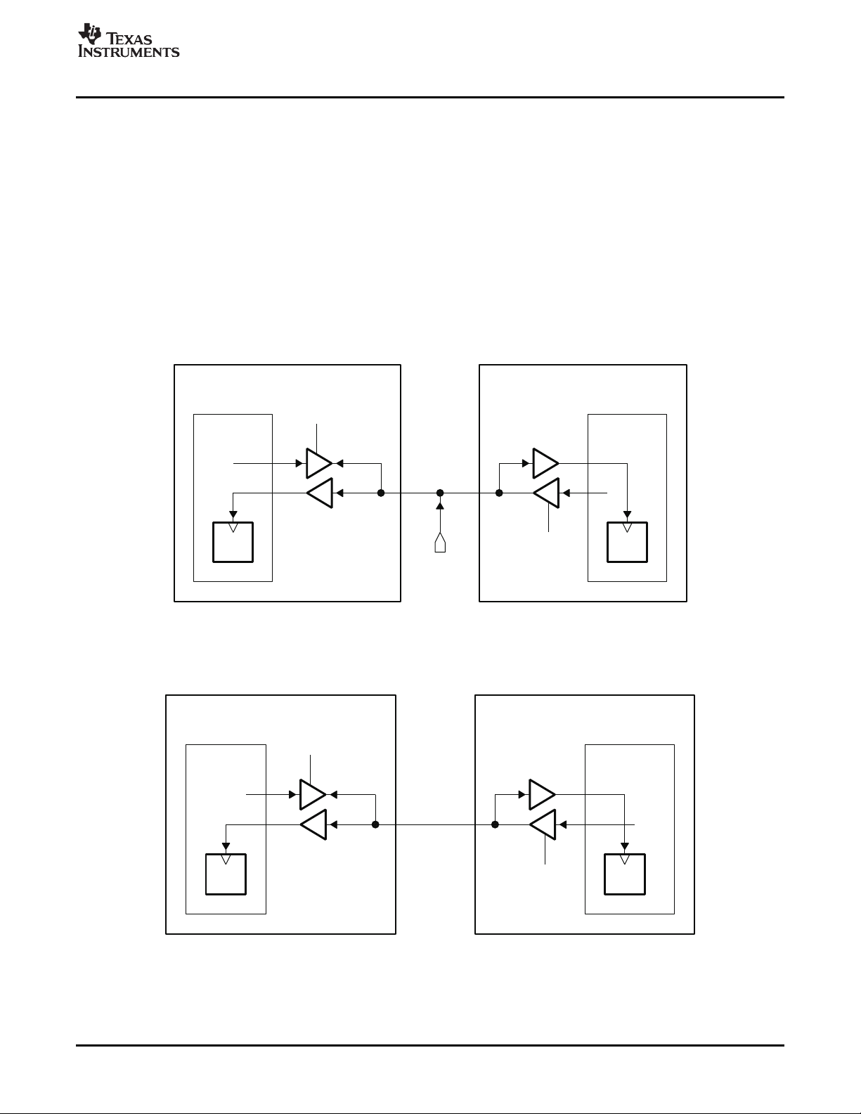
2 Peripheral Architecture
CLKDIR=0
VLYNQ
DMxxxdevice
VLYNQ.CLK
CLKDIR=0
VLYNQ
VLYNQdevice
CLKDIR=1
VLYNQ
DMxxxdevice
VLYNQ.CLK
CLKDIR=0
VLYNQ
VLYNQdevice
Don't
care
VLYNQ
internal
sysclk
2.1 Clock Control
Peripheral Architecture
This section discusses the architecture and basic functions of the VLYNQ peripheral.
The module's serial clock direction and frequency are software configurable through the CLKDIR and
CLKDIV bits in the VLYNQ control register (CTRL). The VLYNQ serial clock can be sourced from the
internal system clock (CLKDIR = 1) or by an external clock source (CLKDIR = 0) for its serial operations.
The CLKDIV bit can divide the serial clock (1/1 - 1/8) down when the internal clock is selected as the
source. The serial clock is not affected by the CLKDIV bit values, if the serial clock is externally sourced.
The reset value of the CLKDIR bit is 0 (external clock source).
The external clock source is shown in Figure 2 . The internal clock source is shown in Figure 3 .
Figure 2. External Clock Block Diagram
SPRUE36A – September 2007 VLYNQ Port 11
Submit Documentation Feedback
Figure 3. Internal Clock Block Diagram
Page 12

www.ti.com
Peripheral Architecture
2.2 Signal Descriptions
The VLYNQ module on the DM644x device is configurable for a 1 to 4 bit-wide RX/TX. Chip-level pin
multiplexing registers control the configuration. See the pin multiplexing information in the device-specific
data manual.
If the configured width does not match the number of transmit/receive lines that are available on the
remote device, negotiation between the two VLYNQ devices automatically configures the width (see
Section 2.7 ).
The VLYNQ interface signals are shown in Table 1 .
Table 1. VLYNQ Port Pins
Pin Name Signal Name I/O Description
VLYNQ_CLOCK VLYNQ serial clock I/O The VLYNQ reference clock supports the internally or externally generated
VLYNQ_SCRUN VLYNQ serial clock I/O The VLYNQ serial clock run request allows remote requests for the VLYNQ
run request serial clock to be turned off for system power management.
(Active low) Low: The request VLYNQ serial clock is active.
VLYNQ_RXD[0:3] VLYNQ receive data I VLYNQ receive data is synchronous with the VLYNQ serial clock.
VLYNQ_TXD[0:3] VLYNQ transmit data O VLYNQ transmit data is synchronous with the VLYNQ serial clock.
clock.
High: The VLYNQ serial clock is requested to be high when all transactions are
complete.
2.3 Pin Multiplexing
2.4 Protocol Description
The VLYNQ signals share pins on the processor package with other processor functions. The VLYNQ
module pins are not enabled at reset. In order to change the default function of device pins at reset, the
pin multiplexing registers (PINMUX n) must be configured appropriately. See the pin multiplexing
information in the device-specific data manual for more detailed information on the processor pin
multiplexing and configuration registers.
VLYNQ relies on 8b/10b block coding to minimize the number of serial pins and allows for in-band packet
delineation and control.
Appendix A provides general information on 8b/10b coding definitions and their implementation within the
VLYNQ module in the DM644x device.
VLYNQ Port12 SPRUE36A – September 2007
Submit Documentation Feedback
Page 13
www.ti.com
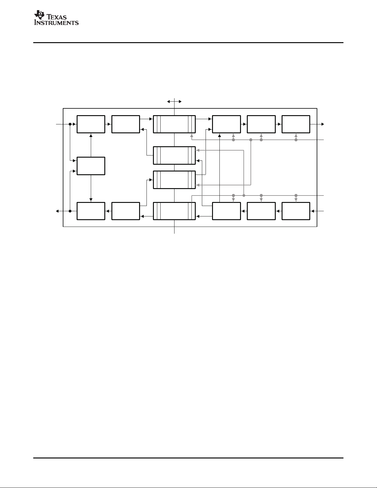
2.5 VLYNQ Functional Description
Address
translation
commands
Outbound
Outbound
command
FIFO
data
Return
FIFO
data
FIFO
Return
command
Inbound
FIFO
Registers
translation
Address
TxSM
8B/10B
encoding
Serializer
commands
Inbound
RxSM Deserializer
decoding
8B/10B
Serial
TxData
Serial
TxClk
Serial
RxClk
Serial
RxData
Master
configbus
interface
Systemclock VLYNQclock
Slave
configbus
interface
(FIFO3)
(FIFO2)
(FIFO0)
(FIFO1)
The VLYNQ core supports both host-to-peripheral and peer-to-peer communication models and is
symmetrical. The VLYNQ module structure is shown in Figure 4 .
Peripheral Architecture
Figure 4. VLYNQ Module Structure
The VLYNQ core module implements two 32-bit configuration bus interfaces. Transmit operations and
control register access require the slave configuration bus interface. The master configuration bus
interface is required for receive operations. Converting to and from the 32-bit bus to the external serial
interface requires serializer and deserializer blocks.
8b/10b block coding encodes data on the serial interface. Frame delineation, initialization, and flow control
use special overhead code groups.
FIFOs buffer the entire burst on the bus for maximum performance, thus minimizing bus latency. Using
write operations of each VLYNQ module interfaced is typically recommended to ensure the best
performance on both directions of the link.
SPRUE36A – September 2007 VLYNQ Port 13
Submit Documentation Feedback
Page 14
www.ti.com
Address
translation
commands
Outbound
Outbound
command
FIFO
data
Return
FIFO
data
FIFO
Return
command
Inbound
FIFO
Registers
translation
Address
TxSM
8B/10B
encoding
Serializer
commands
Inbound
RxSM Deserializer
decoding
8B/10B
Serial
TxData
Serial
RxData
Systemclock
Address
translation
Registers
commands
Inbound
translation
Address
commands
Outbound
8B/10B
decoding
FIFO
FIFO
command
Inbound
data
Return
FIFO
RxSM Deserializer
RxData
Serial
encoding
8B/10B
VLYNQClock
command
Return
data
FIFO
Outbound
TxSM Serializer
TxData
Serial
Slave
configbus
interface
Systemclock VLYNQclock
LocalVLYNQ
RemoteVLYNQ
Master
configbus
interface
Master
configbus
interface
Slave
configbus
interface
Peripheral Architecture
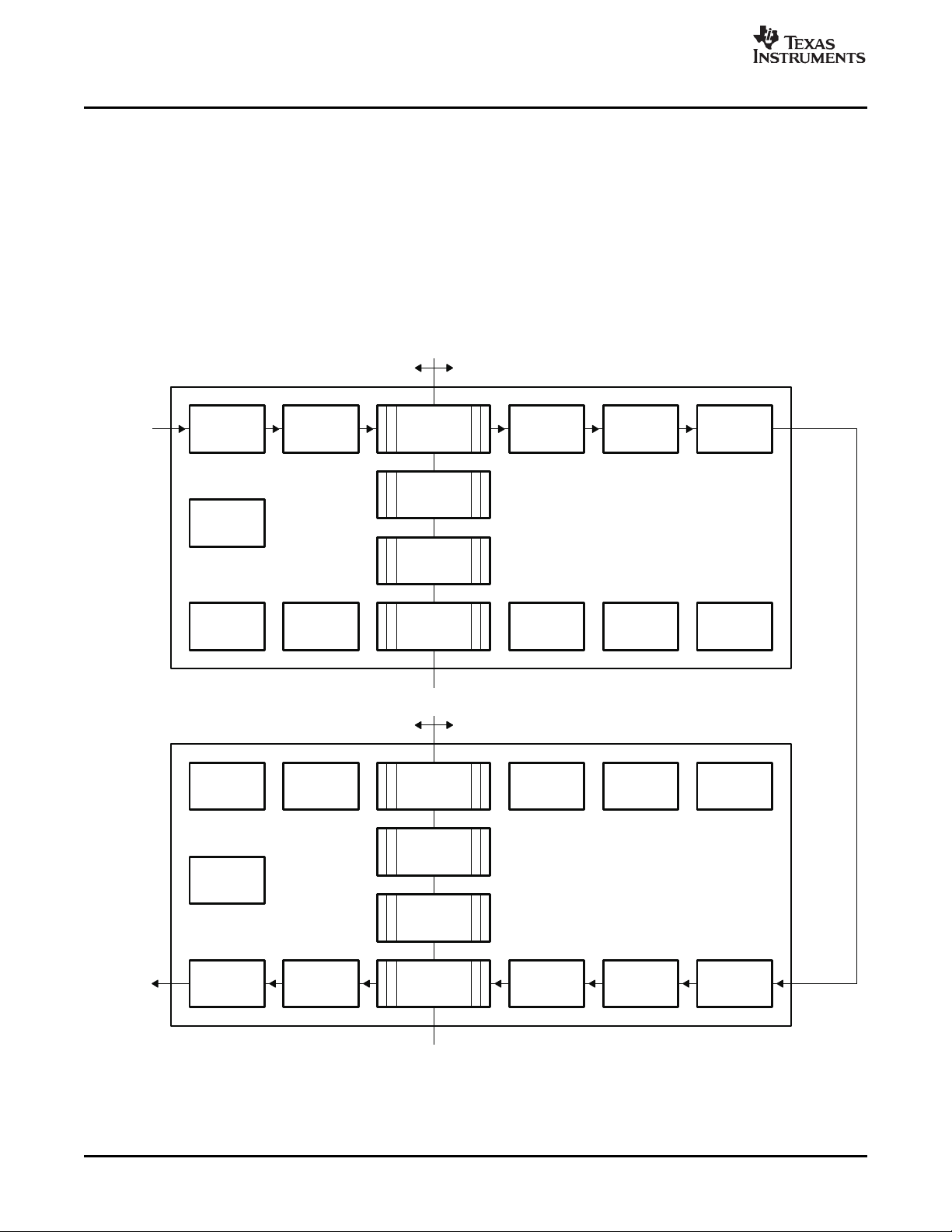
2.5.1 Write Operations
Write requests that initiate from the slave configuration bus interface of the local device write to the
outbound command (CMD) FIFO. Data is subsequently read from the FIFO and encapsulated in a write
request packet. The address is translated, and the packet is encoded and serialized before being
transmitted to remote device. The remote device subsequently deserializes and decodes the receive data
and writes it into the inbound CMD FIFO. A write operation initiates on the remote device’s master
configuration bus interface after reading the address and data from the FIFO.
The data flow between two VLYNQs that are connected is shown in Figure 5 . In the example shown in
Figure 5 , the write originates from the DM644x device.
Figure 5. Write Operations
VLYNQ Port14 SPRUE36A – September 2007
Submit Documentation Feedback
Page 15
www.ti.com
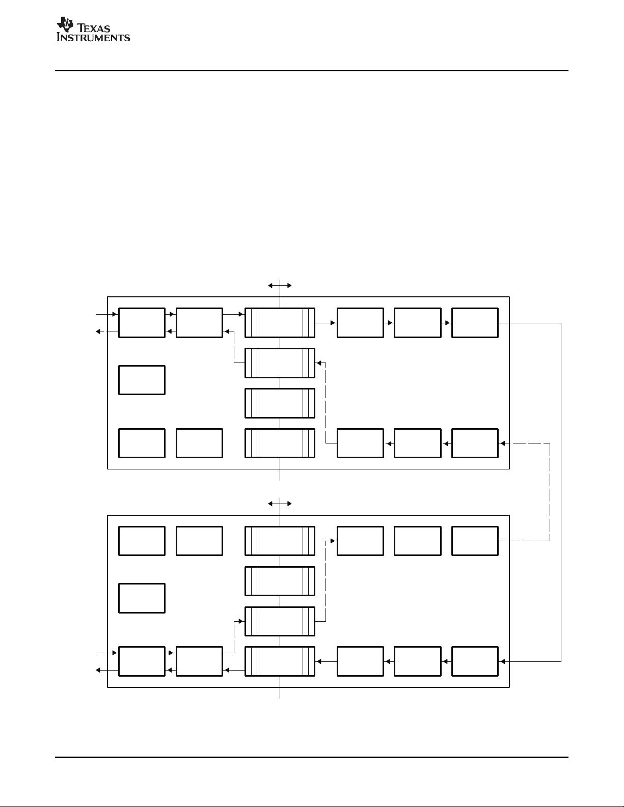
2.5.2 Read Operations
Address
translation
commands
Outbound
Outbound
command
FIFO
data
Return
FIFO
data
FIFO
Return
command
Inbound
FIFO
Registers
translation
Address
TxSM
8B/10B
encoding
Serializer
commands
Inbound
RxSM Deserializer
decoding
8B/10B
Serial
TxData
Serial
RxData
Systemclock
Address
translation
Registers
commands
Inbound
translation
Address
commands
Outbound
8B/10B
decoding
FIFO
FIFO
command
Inbound
data
Return
FIFO
RxSM Deserializer
RxData
Serial
encoding
8B/10B
VLYNQClock
command
Return
data
FIFO
Outbound
TxSM Serializer
TxData
Serial
Slave
configbus
interface
VLYNQClock
Systemclock
LocalVLYNC
RemoteVLYNQ
Master
configbus
interface
Slave
configbus
interface
Master
configbus
interface
Peripheral Architecture
Read requests from the slave configuration bus interface are written to the outbound CMD FIFO (similar to
the write requests). Data is subsequently read from the FIFO and encapsulated into a read request
packet. The packet is encoded and serialized before it is transmitted to the remote device. Next, the
remote device deserializes, decodes the receive data, and writes the receive data to the inbound CMD
FIFO. After reading the address from the FIFO, a master configuration bus interface read operation
initiates in the remote device. When the remote master configuration bus interface receives the read data,
the data is written to the return data FIFO before it is encoded and serialized. When the receive data
reaches the local VLYNQ module, it is deserialized, decoded, and written to the return data FIFO (local
device). Finally, the read data is transferred on the local device’s slave configuration interface.
The data flow between two connected VLYNQ devices with read requests that originate from the DM644x
device is shown in Figure 6 . The remote VLYNQ device returns the read data. Read data is shown with
dotted arrows.
Figure 6. Read Operations
SPRUE36A – September 2007 VLYNQ Port 15
Submit Documentation Feedback
Page 16

www.ti.com
Peripheral Architecture
Note: Not servicing read operations results in deadlock. The only way to recover from a deadlock
situation is to perform a hard reset. Read operations are typically not serviced due to read
requests that are issued to a non-existent remote VLYNQ device or they are not serviced
due to trying to perform reads on the VLYNQ memory map prior to establishing the link.
Generally, you should not use read operations to transfer data packets since the serial nature of the
interface could potentially result in longer latencies. See Appendix B for more information.
2.6 Initialization
Since VLYNQ devices can be controlled solely over the serial interface (that is, no local CPU exists), an
automatic reliable initialization sequence (without user configuration) establishes a connection between
two VLYNQ devices, just after a VLYNQ module is enabled and auto-negotiation occurs. Auto-negotiation
is defined in Section 2.7 . The same sequence is used to recover from error conditions.
Bit 0 in the VLYNQ status register (LINK bit) is set to 1 when a link is established.
A link pulse timer generates a periodic link code every 2048 serial clock cycles. The link is lost when time
expires and no link code has been detected during a period of 4096 serial clock cycles.
2.7 Auto-Negotiation
Auto-negotiation occurs after reset. It involves placing a negotiation protocol in the outbound data and
processing the inbound data to establish connection information. The width of the data pins on the serial
interface is automatically determined at reset as a part of the initialization sequence. For a connection
between two VLYNQ devices of version 2.0 and later (VLYNQ on DM644x device is version 2.6), the
negotiation protocol using the available serial pins is used to convey the maximum width capability of each
device. The TXD data pins are not required to have the same width as the RXD data pins.
The auto width negotiation does not occur until after completion of the VLYNQ 1.x legacy width
configuration, which involves a period of 2000 VLYNQ 1.x system clock cycles for connection to VLYNQ
1.x devices. After the VLYNQ 1.x has determined its width, it receives the VLYNQ2.x auto width
negotiation protocol. The VLYNQ 1.x device does not recognize this protocol and transmits error codes
over the serial interface. The received error codes allow the VLYNQ 2.x devices to determine how many
serial pins are valid on the connected VLYNQ 1.x device.
Once the width is established, VLYNQ further identifies the version (version 1.x or version 2.x ) of the
remote VLYNQ. This better determines the capabilities of the connected VLYNQ device. This is software
readable via the VLYNQ auto-negotiation register (AUTNGO), bit 16 (0 = Ver 1.x , 1 = Ver 2.x), after the
link has been established.
2.8 Serial Interface Width Configuration
The VLYNQWD bit in the pin multiplexing register 0 (PINMUX0) controls the data width on the DM644x
device, thus allowing you to program the serial interface width (as shown in Table 2 ).
Table 2. Serial Interface Width
VLYNQWD VLYNQ Data Width
00 VLYNQ TXD[0] , VLYNQ RXD[0]
01 VLYNQ TXD[0:1] , VLYNQ RXD[0:1]
11 VLYNQ TXD[0:2] , VLYNQ RXD[0:2]
10 VLYNQ TXD[0:3] , VLYNQ RXD[0:3]
For detailed information on the processor pin multiplexing and configuration register, see the pin
multiplexing information in the device-specific data manual.
VLYNQ Port16 SPRUE36A – September 2007
Submit Documentation Feedback
Page 17

www.ti.com
2.9 Address Translation
Peripheral Architecture
Remote VLYNQ device(s) are memory mapped to the local (host) device’s address space when a link is
established (this is similar to any other on-chip peripherals). Enumerating the VLYNQ devices (single or
multiple) into a coherent memory map for accessing each device is part of the initialization sequence.
After the enumeration, the host (local) device can access the remote device address map using local
device addresses. The VLYNQ module in the host device manages the address translation of the local
address to the remote address. A remote VLYNQ device is mapped to the local device’s address via the
address map registers (TX address map, RX address map size n, RX address map offset n, where n = 1
to 4). The transmit side has a contiguous map; the size of the map is the same as the remote device map.
Figure 7 illustrates this mapping.
In the local device, the address of the VLYNQ remote memory map in the local configuration space is the
transmit address accessing remote devices over the serial interface. The address of the VLYNQ remote
memory map is programmed in the TX address map register (XAM). When the local device transmits, first
it strips off the transmit address offset in the local device memory map. Then, the local device sends the
data with an address offset from the transmit address.
VLYNQ allows each receive packet address to be translated into one of the four mapped regions. The size
and offset of each memory region must be aligned to 32-bit words. No restriction is placed on
programming the size or on the offset of each mapped region, as long as the total memory that is mapped
into these one to four regions is not more then 64 MBytes.
Note: Care should be taken while programming the receive address map size register (RAMS n)
and the receive address map offset register (RAMO n) values. These registers should be
programmed with valid address locations and memory size to match the device
specifications. See the Memory Map Summary and the System Interconnect sections in your
device-specific data manual to identify the valid memory regions that can be accessed by an
off-chip peer device through the VLYNQ interface.
The transmitted address is used to determine which remote mapped region is being accessed at the
remote device. This is achieved by summing each memory size sequentially until the memory size is
larger than the transmitted address. The last memory size that is added is the targeted region. A memory
size and an offset specify the remote map. The remote map is programmed in the RX address map size
register (RAMS n) and in the RX address map offset register (RAMO n) in the remote device.
SPRUE36A – September 2007 VLYNQ Port 17
Submit Documentation Feedback
Page 18

www.ti.com
Mapregion1
Mapregion2
Mapregion3
Mapregion4
0400:0000
(0C00:0000onCONFIGbus)
0800:0000
07FF:FFFF
0800:0100
0800:00FF
0801:0100
0801:00FF
0841:00FF
Mapregion1
Mapregion2
Mapregion3
Mapregion4
DMxxxdevice(local)
Remote
VLYNQdevice
0000:0000
03FF:FFFF
0400:0000
0400:00FF
0500:0000
0500:FFFF
0B00:0000
0B3F:FFFF
Peripheral Architecture
Figure 7. Example Address Memory Map
The following shows an example illustrating the address translation used in each VLYNQ module.
Address bits [31:26] are not used for address translation to remote devices on the DM644x device.
Table 3 illustrates address map register configuration when the DM644x device is transmitting data to the
remote device.
Register DM644x VLYNQ Module Remote VLYNQ Module
TX Address Map 0000 : 0000h Do not care
RX Address Map Size 1 Do not care 0000 : 0100h
RX Address Map Offset 1 Do not care 0800 : 0000h
Table 3. Address Translation Example (Single Mapped Region)
VLYNQ Port18 SPRUE36A – September 2007
Submit Documentation Feedback
Page 19

www.ti.com
Peripheral Architecture
DM644x VLYNQ Module:
0C00 : 0054h Initial address at the slave configuration bus
0000 : 0054h Initial address [25:0] at the slave configuration bus interface
subtract 0000 : 0000h TX address map register (there is no need to change the reset value of the
DM644x device for this register)
0000 : 0054h
Remote VLYNQ Module:
0000 : 0054h Initial address from the RX serial interface
compare 0000 : 0100h RX address map size 1 register
0000 : 0054h
add 0800 : 0000h RX address map offset 1 register
0800 : 0054h Translated address to remote device
The local address 0C00 : 0054h (or 0000 0054h) was translated to 0800 : 0054h on the remote VLYNQ
device in Table 4 .
Table 4 illustrates the address map register configuration when the DM644x device is receiving data from
the remote device.
Table 4. Address Translation Example (Single Mapped Region)
Register DM644x VLYNQ Module Remote VLYNQ Module
TX Address Map Do not care 0400 : 0000h
RX Address Map Size 1 0000 : 0100h Do not care
RX Address Map Offset 1 0200 : 0000h Do not care
RX Address Map Size 2 0000 : 0100h Do not care
RX Address Map Offset 2 8200 : 0000h Do not care
Remote VLYNQ Module:
0400 : 0154h Initial address at the slave configuration bus for the remote device
subtract 0400 : 0000h TX address map register
0000 : 0154h Translated address to remote device via serial interface
DM644x VLYNQ Module:
0000 : 0154h Initial address from the RX serial interface
compare 0000 : 0100h RX address map size 1 register
0000 : 0154h The RX packet address is greater than the value in the RX address map size 1
register
compare 0000 : 0200h RX address map size 1 register + RX address map size 2
Since the RX packet address < the RX address map size 1 register +
RX address map size 2 register
add 8200 : 0000h RX address map offset 2 register
subtract 0000 : 0100h RX address map size 1 register
8200 : 0054h Translated address to DM644x device
SPRUE36A – September 2007 VLYNQ Port 19
Submit Documentation Feedback
Page 20

www.ti.com
Peripheral Architecture
Example 1. Address Translation Example
The remote address 0x 0400 : 0154 (or 0x0000 0054) was translated to 0x 8200 : 0054 on the DM644x
(local) device in this example.
The translated address for packets received on the serial interface is determined as follows:
If ( RX Packet Address < RX Address Map Size 1 Register) {
Translated Address = RX Packet Address +
RX Address Map Offset 1 Register
} else if ( RX Packet Address < (RX Address Map Size 1 Register +
Translated Address = RX Packet Address +
} else if ( RX Packet Address < (RX Address Map Size 1 Register +
Translated Address = RX Packet Address +
RX Address Map Offset 3 Register -
} else if ( RX Packet Address < (RX Address Map Size 1 Register +
Translated Address = RX Packet Address +
RX Address Map Offset 4 Register -
} else {
Translated Address = 0x0
}
RX Address Map Size 2 Register)) {
RX Address Map Offset 2 Register RX Address Map Size 1 Register
RX Address Map Size 2 Register +
RX Address Map Size 3 Register)) {
RX Address Map Size 1 Register RX Address Map Size 2 Register
RX Address Map Size 2 Register +
RX Address Map Size 3 Register +
RX Address Map Size 4 Register)) {
RX Address Map Size 1 Register RX Address Map Size 2 Register RX Address Map Size 3 Register
2.10 Flow Control
The VLYNQ module includes flow control features. The VLYNQ module automatically generates flow
control enable requests, /P/, when the RX/inbound FIFOs (FIFO1 and FIFO2) resources are consumed.
The FIFOs can take up to 16 32-bit words.
The remote device will begin transmitting idles, /I/, starting on the first byte boundary following reception of
the request. When sufficient RX FIFO resources have been made available, a flow control disable request,
/C/, is transmitted to the remote device. In response, the remote device will resume transmission of data.
See Appendix A .
VLYNQ Port20 SPRUE36A – September 2007
Submit Documentation Feedback
Page 21

www.ti.com
2.11 Reset Considerations
2.11.1 Software Reset Considerations
Peripheral clock and reset control is done through the power and sleep controller (PSC) module that is
included with the device. For more information, refer to the power management section (Section 2.14 ).
Additionally, there is a software reset (the reset bit in the VLYNQ control register, CTRL) within the
peripheral itself. Writing a 1 to the reset bit resets all of the internal state machines of the VLYNQ module,
the serial interface is disabled, and the link is lost. The VLYNQ module remains in reset until the software
clears the bit.
2.11.2 Hardware Reset Considerations
When a hardware reset occurs, the VLYNQ peripheral resets its register values to the default values and
the serial interface is disabled. After a hardware reset, the VLYNQ memory mapped registers and any
chip-level registers that are associated with VLYNQ (for example, pin multiplexing registers) must be
configured appropriately before data transmission can resume.
Peripheral Architecture
Note: When setting the reset bit, the VLYNQ status register (STAT) value is the only value that is
set to the default value. All of the other VLYNQ memory-mapped registers retain their values
prior to the software reset.
CAUTION
Be cautious when only resetting one of the VLYNQ devices after two or more
VLYNQ devices have established a link. If only one of the VLYNQ devices is in
reset, then no data activity can occur across the serial interface during the time
of reset.
2.12 Interrupt Support
2.12.1 Interrupt Events and Requests
The VLYNQ module interrupt VLQINT is mapped to the ARM interrupt controller (ARM INT31). For more
information on the ARM interrupt controller (AINTC), see the TMS320DM644x DMSoC ARM Subsystem
Reference Guide (SPRUE14 ).
Interrupts generate when bits are set in the VLYNQ interrupt pending/set register (INTPENDSET). Bits are
set in the INTPENDSET register when any of the following occur:
• Writing directly to the INTPENDSET
• Remote interrupt (via the serial interrupt packet)
• Serial bus error
When the VLYNQ interrupt pending/set register (INTPENDSET) is a non-zero value, the method of
forwarding the interrupt status depends on the state of the INTLOCAL bit in the VLYNQ control register
(CTRL).
When INTLOCAL = 0, the contents of INTPENDSET are inserted into an interrupt packet and sent over
the serial interface. When packet transmission completes, the associated bits clear in INTPENDSET.
When INTLOCAL = 1, bits in INTPENDSET transfer to the VLYNQ interrupt status/clear register
(INTSTATCLR). The logical-OR of all of the bits in INTSTATCLR is driven onto the interrupt line, causing
the VLYNQINT to pulse.
If the system writes to INTSTATCLR while interrupts are still pending, a new VLQINT interrupt is
generated.
The VLYNQ interrupt generation mechanism is shown in Figure 8 .
SPRUE36A – September 2007 VLYNQ Port 21
Submit Documentation Feedback
Page 22

www.ti.com
VLYNQinterrupt
pending/setregister
(INTPENDSET)
VLYNQ
Status/clear
register
(INTSTATCLR)
OR
Transmitserial
interruptpacket
VLQINT
(ARMINT31)
14 0
INTLOCAL
VLYNQcontrolregister(CTRL)
Serialbuserror
(LERROR/RERROR)
CPUwrites
Serialinterrupt
packetfrom
remotedevice
INTLOCAL=1
INTLOCAL=0
Peripheral Architecture
Figure 8. Interrupt Generation Mechanism Block Diagram
2.12.2 Writes to Interrupt Pending/Set Register
For additional flexibility of interrupt handling, there is an interrupt priority vector status/clear register
(INTPRI) that reports the highest priority interrupt asserted in the VLYNQ interrupt pending/set register
(INTPENDSET) when INTLOCAL = 1. VLYNQ interprets bit 0 as the highest priority and it interprets bit 31
as the lowest priority. The value that is returned when read is the vector of the highest priority interrupt.
Software can clear that interrupt by writing back the vector value. Additionally, INTRPRI provides a
read-only status bit (NOINTPEND) to indicate whether or not there are any pending interrupts in the
interrupt status/clear register (INTSTATCLR).
As previously discussed, if the ARM CPU writes to the VLYNQ interrupt pending/set register
(INTPENDSET), then depending on the value of the INTLOCAL bit in the VLYNQ control (CTRL) register,
this will result in a local interrupt (to the device interrupt controller) or an interrupt packet transmitted over
the serial interface to the remote device.
VLYNQ Port22 SPRUE36A – September 2007
Submit Documentation Feedback
Page 23

www.ti.com
2.12.3 Remote Interrupts
Remote interrupts occur when an interrupt packet is received over the serial interface from a remote
device. The interrupt status is extracted from the packet and written to a location pointed to by the
interrupt pointer register (INTPTR).
The INTPTR should contain the address of the interrupt pending/set register (INTPENDSET). To get
INTPTR to contain the address of INTPENDSET, program INTPTR with a value of 14h (the offset for
INTPENDSET). Additionally, the INT2CFG bit in the VLYNQ control register (CTRL) must be set to 1,
dictating that the VLYNQ writes to a local register space (in this case, INTPENDSET).
Once an interrupt packet is received over the serial interface, the interrupt status is extracted and written
to INTPENDSET. After the interrupt status is extracted and written to INTPENDSET, the interrupt
generation occurs as previously described in Section 2.12.2 .
The following summarizes the steps that are required to ensure that the device receives the remote
interrupts:
• Program the VLYNQ interrupt pointer register (INTRPTR) with a value of 14h, which is the offset
address of the VLYNQ interrupt/pending set register (INTPENDSET).
• Set the INT2CFG bit to 1 in the VLYNQ control register (CTRL).
2.12.4 Serial Bus Error Interrupts
Due to erroneous transmit packets that are detected by remote devices (remote error) or errors in the
inbound packets (local error), the serial bus errors result in the setting of the RERROR or LERROR bits in
the VLYNQ status register (STAT).
Additionally, if the INTENABLE bit is set in the VLYNQ control register (CTRL), setting the RERROR or
LERROR bits cause these status interrupts to post to the interrupt pending/set register (INTPENDSET),
causing the VLYNQINT to be asserted to the ARM CPU.
To ensure that serial bus errors result in interrupts to notify the application software, you must perform the
following steps:
1. Set the INTENABLE bit to 1 in the VLYNQ control register (CTRL).
2. Set the INTVEC bits in CTRL to point to a free bit in the VLYNQ interrupt pending/set register
(INTPENDSET). The serial bus error should result in setting the bits in INTPENDSET that are not used
by the application software for other interrupts (bit locations written directly in INTPENDSET or via
remote interrupts).
3. During VLYNQ initialization, the RERROR bit is set after the VLYNQ module achieves a link. When the
link bit is set in the VLYNQ status register (STAT), write a 1 to the RERROR bit. Writing a 1 to the
RERROR bit clears the RERROR bit and prevents the software interrupt handler from seeing the first
RERROR as a legitimate serial bus error interrupt.
Peripheral Architecture
2.13 DMA Event Support
The VLYNQ module on the DM644x device is classified as a master peripheral. Classification as a master
peripheral normally implies that the peripheral is able to sustain its own transfers without relying on any
external peripherals (for example, the system DMA, etc). However, the VLYNQ module does not have an
internal DMA (as some other master peripherals).
Therefore, it is likely that the VLYNQ module can rely on the on-chip enhanced DMA (EDMA3) controller
for performing burst transfer. The EDMA3 can still be used to perform burst transfers out to remote
VLYNQ memory map (writes). This use model provides better throughput with less overhead.
Note: There is no VLYNQ event that allows hardware synchronization to occur with the EDMA3
controller on the DM644x device.
The VLYNQ module uses a 16-word deep FIFO to buffer the burst writes. Since the EDMA3 controller is
much faster compared to the serial VLYNQ interface, a data back-up can occur. Therefore, configuring
EDMA3 for optimal transfer size, etc. is essential.
SPRUE36A – September 2007 VLYNQ Port 23
Submit Documentation Feedback
Page 24

www.ti.com
Peripheral Architecture
2.14 Power Management
The VLYNQ module can be placed in reduced-power modes to conserve power during periods of low
activity. The power management of the peripheral is controlled by the processor Power and Sleep
Controller (PSC). The PSC acts as a master controller for power management of all of the peripherals on
the processor.
The power conservation modes that are available via the PSC are:
• Idle/Disabled state : Idle/disabled state stops the clocks from going to the peripheral and prevents all of
the register accesses. After re-enabling the peripheral from its idle state, all registers prior to setting in
the disabled state are restored and data transmission proceeds. Re-initialization is not required.
• Synchronized reset : The synchronized reset state is similar to the power-on reset (POR) state. When
the processor is turned on, reset to the peripheral is asserted, then clocks to the peripheral are gated.
Registers reset to their default values. When powering-up after a synchronized reset, all of the VLYNQ
module registers must be reconfigured and the link must be re-established before data transmission.
For more detailed information on power management procedures using the PSC, see the
TMS320DM644x DMSoC ARM Subsystem Reference Guide (SPRUE14 ).
If the serial clock is internally sourced, you can use the CLKDIV bit in the VLYNQ control register (CTRL)
to divide the serial clock down. This saves normal mode operation power consumption (at the expense of
reduced performance).
Additionally, the module provides the capability of auto-idling the serial clock domain (disable the VLYNQ
CLK) when the serial clock is sourced from the DM644x device and the VLYNQ SCRUN pin is connected
to the remote device. This allows power savings when there is no activity on the serial interface.
Note: There is no support for external wake-up for the VLYNQ module on the DM644x device. If
the VLYNQ module on the DM644x device has been disabled via the PSC, then even though
serial activity requests can be indicated from the remote VLYNQ device via the VLYNQ
SCRUN pin, it does not allow the serial clock (VLYNQ CLK) to be sourced until the VLYNQ
module is re-enabled via the PSC.
This can be configured by enabling the power management enable (PMEN) bit in the VLYNQ control
registers (CTRL, 0 = disable, 1 = enable) . This bit should only be set if the SCRUN pin is connected to
the remote VLYNQ device.
The SCRUN pin is a bi-directional pin which is driven low whenever there is serial activity on the local or
remote VLYNQ interface.
2.15 Emulation Considerations
During debug, the ARM CPU may be halted for single stepping, bench marking, profiling, or other debug
uses using the emulator. VLYNQ does not support emulation halts/suspend operation. VLYNQ operations
continue during emulation halt/suspend.
VLYNQ Port24 SPRUE36A – September 2007
Submit Documentation Feedback
Page 25

www.ti.com
3 VLYNQ Port Registers
Table 5 describes the address space for the VLYNQ registers and memory.
Block Name Start Address End Address Size
VLYNQ Control Registers 01E0 1000h 01E0 11FFh 512 bytes
Reserved 01E0 1200h 01E0 1FFFh VLYNQ Remote Memory Map 0C00 0000h 0CFF FFFFh 64 Mbytes
Table 6 lists the memory-mapped registers for the VLYNQ port controller. See the device-specific data
manual for the memory address of these registers.
The first 128 bytes map to the VLYNQ configuration registers that are maintained by the local (device)
VLYNQ register control module while the second 128 bytes map to the remote configuration registers that
are physically located in the remote device linked by the VLYNQ serial interface. Any access to the
second set of registers causes VLYNQ to issue a read or write VLYNQ packet to be transmitted and only
completes if a link is established between the two devices.
VLYNQ Port Registers
Table 5. VLYNQ Register Address Space
Table 6. VLYNQ Port Controller Registers
Offset Acronym Register Description Section
0h REVID Revision Register Section 3.1
4h CTRL Control Register Section 3.2
8h STAT Status Register Section 3.3
Ch INTPRI Interrupt Priority Vector Status/Clear Register Section 3.4
10h INTSTATCLR Interrupt Status/Clear Register Section 3.5
14h INTPENDSET Interrupt Pending/Set Register Section 3.6
18h INTPTR Interrupt Pointer Register Section 3.7
1Ch XAM Transmit Address Map Register Section 3.8
20h RAMS1 Receive Address Map Size 1 Register Section 3.9
24h RAMO1 Receive Address Map Offset 1 Register Section 3.10
28h RAMS2 Receive Address Map Size 2 Register Section 3.11
2Ch RAMO2 Receive Address Map Offset 2 Register Section 3.12
30h RAMS3 Receive Address Map Size 3 Register Section 3.13
34h RAMO3 Receive Address Map Offset 3 Register Section 3.14
38h RAMS4 Receive Address Map Size 4 Register Section 3.15
3Ch RAMO4 Receive Address Map Offset 4 Register Section 3.16
40h CHIPVER Chip Version Register Section 3.17
44h AUTNGO Auto Negotiation Register Section 3.18
SPRUE36A – September 2007 VLYNQ Port 25
Submit Documentation Feedback
Page 26

www.ti.com
VLYNQ Port Registers
3.1 Revision Register (REVID)
The revision register (REVID) contains the major and minor revisions for the VLYNQ module. The REVID
is shown in Figure 9 and described in Table 7 .
Figure 9. Revision Register (REVID)
31 16
ID
R-1h
15 8 7 0
REVMAJ REVMIN
R-2h R-6h
LEGEND: R = Read only; - n = value after reset
Table 7. Revision Register (REVID) Field Descriptions
Bit Field Value Description
31-16 ID 01h Unique module ID.
15-8 REVMAJ 0-FFh Major revision.
2h Current major revision.
7-0 REVMIN 0-FFh Minor revision.
6h Current minor revision.
26 VLYNQ Port SPRUE36A – September 2007
Submit Documentation Feedback
Page 27

www.ti.com
VLYNQ Port Registers
3.2 Control Register (CTRL)
The control register (CTRL) determines operation of the VLYNQ module. The CTRL is shown in Figure 10
and described in Table 8 .
Figure 10. Control Register (CTRL)
31 30 29 27 26 24 23 22 21 20 19 18 16
PMEN SCLKPUDIS Reserved RXSAMPELVAL RTMVALIDWR RTMENABLE TXFASTPATH Reserved CLKDIV
R/W- 0 R/W- 0 R-0 R/W- 3h R/W- 0 R/W- 0 R/W- 0 R-0 R/W- 0
15 14 13 12 8 7 6 3 2 1 0
CLKDIR INTLOCAL INTENABLE INTVEC INT2CFG Reserved AOPTDISABLE ILOOP RESET
R/W- 0 R/W- 0 R/W- 0 R/W-0 R/W-0 R-0 R/W- 0 R/W- 0 R/W- 0
LEGEND: R/W = Read/Write; R = Read only; - n = value after reset
Table 8. Control Register (CTRL) Field Descriptions
Bit Field Value Description
31 PMEN Power management enable.
0 VLYNQ CLK is always active if it is set as an output (assuming that VLYNQ module is enabled).
If set as an output, VLYNQ CLK becomes inactive when there is no traffic over the serial bus.
1
The PMEN bit should only be set to 1 when the SCRUN is connected to the remote/external
VLYNQ device.
30 SCLKPUDIS 0 Serial clock pull-up disable. Always write 0.
29-27 Reserved 0 Reserved. Always read as 0. Writes have no effect.
26-24 RXSAMPELVAL 0-7h RTM sample value. If the RTMENABLE bit is 0, the receive timing manager forces the value in the
23 RTMVALIDWR RTM valid write bit.
22 RTMENABLE RTM enable bit.
21 TXFASTPATH 0-1 Transmit fast path. When set, the fastest path is chosen for the serial data.
20-19 Reserved 0 Reserved. Always read as 0. Writes have no effect.
18-16 CLKDIV 0-7h Serial clock output divider.
15 CLKDIR Serial CLK direction. Determines whether the VLYNQ CLK is an input or an output.
14 INTLOCAL Interrupt local.
13 INTENABLE Interrupt enable.
12-8 INTVEC 0-1Fh Interrupt vector. This bit indicates which bit in the interrupt pending/set register is set for VLYNQ
RXSAMPELVAL bit as the clock sample value. If the RTMENABLE bit is 1, then the value set by
the RXSAMPELVAL bit is ignored. In order to modify the value, you must simultaneously write a 1
to the RTMVALIDWR bit.
0 Will not allow writes to RXSAMPLEVAL bits.
1 Will allow writes to RXSAMPLEVAL bits.
The receive timing manager uses the value set in the RXSAMPLEVAL bit as the clock sample
0
value.
1 The receive timing manager is enabled. It automatically selects the receive clock.
0 The VLYNQ CLK is externally sourced.
The VLYNQ CLK is internally sourced and equal to the VLYNQ module system clock divided by the
1
divider value set in the CLKDIV bit.
0 The interrupt is forwarded to the remote VLYNQ device over the serial interface as an interrupt
packet.
Interrupt is posted in the interrupt status/clear register and results in the assertion of the VLQINT to
1
the device interrupt controllers.
0 VLYNQ module status interrupts are ignored.
VLYNQ module status interrupts (if RERROR or LERROR bits are set) are posted to the interrupt
1
pending/set register.
module status (RERROR/LERROR) interrupts.
SPRUE36A – September 2007 VLYNQ Port 27
Submit Documentation Feedback
Page 28

www.ti.com
VLYNQ Port Registers
Table 8. Control Register (CTRL) Field Descriptions (continued)
Bit Field Value Description
7 INT2CFG Interrupt to configuration register. Determines which register is written with the status contained in
6-3 Reserved 0 Reserved. Always read as 0. Writes have no effect.
2 AOPTDISABLE Address optimization disable.
1 ILOOP Internal loop back.
0 RESET Software reset. It does not reset the VLYNQ MMR registers (except for the VLYNQ status register).
interrupt packets that are received over the serial interface. Always write 1 to this bit and configure
the interrupt pointer register to point to the interrupt pending/set register.
0 Bits[31:2] of the interrupt pointer register are used to point to a system interrupt register.
1 The least significant 8 bits of the interrupt pointer register are used to point to a VLYNQ module
local register (typically the interrupt pending/set register).
0 Address optimization is enabled, eliminating unnecessary address bytes.
1 Address optimization is disabled.
0 Normal operation.
1 Serial transmit data is wrapped back to the serial receive data.
You have to reprogram the VLYNQ MMRs if they must have a different value after a software reset.
0 Normal operation.
1 All internal state machines are reset, the serial interface is disabled, and the link is lost.
28 VLYNQ Port SPRUE36A – September 2007
Submit Documentation Feedback
Page 29

www.ti.com
VLYNQ Port Registers
3.3 Status Register (STAT)
The status register (STAT) is used to detect conditions that may be of interest to the system designer. The
STAT is shown in Figure 11 and described in Table 9 .
Figure 11. Status Register (STAT)
31 28 27 24 23 20 19 15
Reserved SWIDTHIN SWIDTHOUT Reserved
R-0 R-0 R-0 R-0
14 12 11 10 9 8
RXCURRENTSAMPLE RTM IFLOW OFLOW RERROR
R-0 R-1 R-0 R-0 W1C-0
7 6 5 4 3 2 1 0
LERROR NFEMPTY3 NFEMPTY2 NFEMPTY1 NFEMPTY0 SPEND MPEND LINK
W1C-0 R-0 R-0 R-0 R-0 R-0 R-0 R-0
LEGEND: R/W = Read/Write; R = Read only; W1C = Write 1 to clear bit; - n = value after reset; x= reset value is indeterminate
Table 9. Status Register (STAT) Field Descriptions
Bit Field Value Description
31-28 Reserved 0 Reserved. Always read as 0. Writes have no effect.
27-24 SWIDTHIN Size of the inbound serial data. Indicates the number of receive pins that are being used to
23-20 SWIDTHOUT 0-Fh Size of the outbound serial data. Indicates the number of transmit pins that are being used
19-15 Reserved 0 Reserved. Always read as 0. Writes have no effect.
14-12 RXCURRENTSAMPLE 0-Fh Current RTM sample. Indicates the current clock sample value used by RTM.
11 RTM 1 RTM enable. Always read as 1. Indicates that the VLYNQ module on the DM644x DMSoC
10 IFLOW Inbound flow control.
9 OFLOW Outbound flow control. Indicates the status of the two inbound FIFOs (FIFO1 or FIFO2).
0-Fh
establish the serial interface.
0 No pins used
1h 1 RX pin used
2h 2 RX pins used
3h 3 RX pins used
4h 4 RX pins used
5h-Fh Reserved
to establish the serial interface.
0 No pins used
1h 1 TX pin used
2h 2 TX pins used
3h 3 TX pins used
4h 4 TX pins used
5h-Fh Reserved
has the receive timing manager (RTM).
0 Free to transmit.
Indicates that a flow control enable request has been received and has stalled transmit until
1
a flow control disable request is received.
0 Indicates that the internal flow control threshold is not yet reached.
Indicates that the internal flow control threshold has been reached (FIFO1 or FIFO2 is full)
1
and a flow control enable request has been sent to the remote device.
SPRUE36A – September 2007 VLYNQ Port 29
Submit Documentation Feedback
Page 30

www.ti.com
VLYNQ Port Registers
Table 9. Status Register (STAT) Field Descriptions (continued)
Bit Field Value Description
8 RERROR Remote Error. Write a 1 to this bit to clear it.
0 No error
This bit indicates that a downstream VLYNQ module has detected a packet error. This bit is
1
set when an error indication, /E/, is received from the serial interface. See Appendix A .
If this bit is set, and the INTENABLE (bit 13 in VLYNQ control register) is also set, it asserts
the VLYNQ interrupt (VLQINT).
7 LERROR Local error. Write a 1 to this bit to clear it.
0 No error.
This bit indicates that an inbound packet contains an error that is detected by the local
1
VLYNQ module.
If this bit is set, and the INTENABLE (bit 13 in VLYNQ control register) is also set, it asserts
the VLYNQ interrupt (VLQINT).
6 NFEMPTY3 FIFO 3 is not empty.
0 Indicates that the slave command FIFO is empty.
1 Indicates that the slave command FIFO is not empty.
5 NFEMPTY2 FIFO 2 is not empty.
0 Indicates that the slave data FIFO is empty.
1 Indicates that the slave data FIFO is not empty.
4 NFEMPTY1 FIFO 1 is not empty.
0 Indicates that the master command FIFO is empty.
1 Indicates that the master command FIFO is not empty.
3 NFEMPTY0 FIFO 0 is not empty.
0 Indicates that the master data FIFO is empty.
1 Indicates that the master data FIFO is not empty.
2 SPEND Pending slave request.
0 No pending slave requests.
Indicates detection of a transfer request initiated by the VLYNQ module to the off-chip
1
peripheral (TX slave configuration bus interface).
1 MPEND Pending master requests.
0 No pending master requests.
Indicates detection of a transfer request initiated by an off-chip peripheral to the VLYNQ
1
module (RX master configuration bus interface).
0 LINK Link
0 Indicates that the serial interface initialization sequence has not yet completed or the link
has timed out.
1 Indicates that the serial interface initialization sequence has completed successfully.
30 VLYNQ Port SPRUE36A – September 2007
Submit Documentation Feedback
Page 31

www.ti.com
VLYNQ Port Registers
3.4 Interrupt Priority Vector Status/Clear Register (INTPRI)
The interrupt priority vector status/clear register (INTPRI) displays the highest priority vector with a
pending interrupt when read. When writing, only bits [4:0] are valid, and the value represents the vector of
the interrupt to be cleared. The INTPRI is shown in Figure 12 and described in Table 10 .
Figure 12. Interrupt Priority Vector Status/Clear Register (INTPRI)
31 30 16
NOINTPEND Reserved
R-1h R-0
15 5 4 0
Reserved INSTAT
R-0 R/W-0
LEGEND: R/W = Read/Write; R = Read only; - n = value after reset
Table 10. Interrupt Priority Vector Status/Clear Register (INTPRI) Field Descriptions
Bit Field Value Description
31 NOINTPEND Interrupt pending status.
0 Indicates there is a pending interrupt.
1 Indicates that there are no pending interrupts from the interrupt status/clear register.
30-5 Reserved 0 Reserved. Always read as 0. Writes have no effect.
4-0 INSTAT 0-1Fh pending from the interrupt status/clear register, with bit 0 as the highest priority, and bit 31 as the
When read, this field displays the vector that is mapped to the highest priority interrupt bit that is
lowest. Writing the vector value back to this field clears the interrupt.
3.5 Interrupt Status/Clear Register (INTSTATCLR)
The interrupt status/clear register (INTSTATCLR) indicates the unmasked interrupt status. The
INTSTATCLR is shown in Figure 13 and described in Table 11 .
Figure 13. Interrupt Status/Clear Register (INTSTATCLR)
31 0
INTCLR
R/W-0
LEGEND: R/W = Read/Write; - n = value after reset
Table 11. Interrupt Status/Clear Register (INTSTATCLR) Field Descriptions
Bit Field Value Description
31-0 INTCLR 0-FFFF FFFFh This field indicates the unmasked status of each interrupt. Writing a 1 to any set bit in this field
clears the corresponding interrupt. If there is a bit set in this register and if the INTLOCAL bit in
the control register (CTRL) is also set, the VLYNQ interrupt (VLQINT) is asserted.
SPRUE36A – September 2007 VLYNQ Port 31
Submit Documentation Feedback
Page 32

www.ti.com
VLYNQ Port Registers
3.6 Interrupt Pending/Set Register (INTPENDSET)
The interrupt pending/set register (INTPENDSET) indicates the pending interrupt status when the
INTLOCAL bit in the control register (CTRL) is not set. When the interrupt packet is forwarded on the
serial interface, these bits are cleared. The INTPENDSET is shown in Figure 14 and described in
Table 12 .
Figure 14. Interrupt Pending/Set Register (INTPENDSET)
31 0
INTSET
R/W-0
LEGEND: R/W = Read/Write; - n = value after reset
Table 12. Interrupt Pending/Set Register (INTPENDSET) Field Descriptions
Bit Field Value Description
31-0 INTSET 0-FFFF FFFFh This field indicates the unmasked status of each pending interrupt.
0 Writing a 0 has no effect.
1 Writing a 1 to any bit:
if INTLOCAL = 0 in CTRL, interrupt packet is sent on the serial interface.
If INTLOCAL = 1 in CTRL, VLYNQ module interrupt (VLQINT) is asserted.
3.7 Interrupt Pointer Register (INTPTR)
The interrupt pointer register (INTPTR) typically contains the address of the interrupt pending/set register
(INTPENDSET) within the VLYNQ module. To program INTPTR to point to INTPENDSET, program a
value of 14h (the offset of INTPENDSET). Additionally, the INT2CFG bit in the control register (CTRL)
should be set to 1. The INTPTR is shown in Figure 15 and described in Table 13 .
Figure 15. Interrupt Pointer Register (INTPTR)
31 2 1 0
INTPTR Reserved
R/W-0 R-0
LEGEND: R/W = Read/Write; R = Read only; - n = value after reset
Table 13. Interrupt Pointer Register (INTPTR) Field Descriptions
Bit Field Value Description
31-2 INTPTR 0-3FFF FFFFh Interrupt pointer. Program this register with the address of the interrupt pending/set register
1-0 Reserved 0 Reserved. Always read as 0. Writes have no effect.
(14h).
32 VLYNQ Port SPRUE36A – September 2007
Submit Documentation Feedback
Page 33

www.ti.com
VLYNQ Port Registers
3.8 Transmit Address Map Register (XAM)
The transmit address map register (XAM) is used to translate transmit packet addresses to remote device
configuration bus addresses. The XAM is shown in Figure 16 and described in Table 14 .
Figure 16. Transmit Address Map Register (XAM)
31 2 1 0
TXADRMAP Reserved
R/W-0 R-0
LEGEND: R/W = Read/Write; R = Read only; - n = value after reset
Table 14. Address Map Register (XAM) Field Descriptions
Bit Field Value Description
31-2 TXADRMAP 0-3FFF FFFFh This field is subtracted from the slave configuration bus address [25:0] to obtain the zero
1-0 Reserved 0 Reserved. Always read as 0. Writes have no effect.
relative transmit packet address. This field should be programmed with a value of 0 (reset
value).
SPRUE36A – September 2007 VLYNQ Port 33
Submit Documentation Feedback
Page 34

www.ti.com
VLYNQ Port Registers
3.9 Receive Address Map Size 1 Register (RAMS1)
The receive address map size 1 register (RAMS1) is used to identify the intended destination of inbound
serial packets. The RAMS1 is shown in Figure 17 and described in Table 15 .
Figure 17. Receive Address Map Size 1 Register (RAMS1)
31 2 1 0
RXADRSIZE1 Reserved
R/W-0 R-0
LEGEND: R/W = Read/Write; R = Read only; - n = value after reset
Table 15. Receive Address Map Size 1 Register (RAMS1) Field Descriptions
Bit Field Value Description
31-2 RXADRSIZE1 0-3FFF FFFFh The RXADRSIZE1 field is used to determine if receive packets are destined for the first of
1-0 Reserved 0 Reserved. Always read as 0. Writes have no effect.
four mapped address regions. RXADRSIZE1 is compared with the address contained in the
receive packet. If the received packet address is less than the value in RXADRSIZE1, the
packet address is added to the receive address map offset 1 register (RAMO1) to obtain the
translated address.
3.10 Receive Address Map Offset 1 Register (RAMO1)
The receive address map offset 1 register (RAMO1) is used with the receive address map size 1 register
(RAMS1) to translate receive packet addresses to local device configuration bus addresses. The RAMO1
is shown in Figure 18 and described in Table 16 .
Figure 18. Receive Address Map Offset 1 Register (RAMO1)
31 2 1 0
RXADROFFSET1 Reserved
R/W-0 R-0
LEGEND: R/W = Read/Write; R = Read only; - n = value after reset
Table 16. Receive Address Map Offset 1 Register (RAMO1) Field Descriptions
Bit Field Value Description
31-2 RXADROFFSET1 0-3FFF FFFFh The RXADROFFSET1 field is used with the receive address map size 1 register (RAMS1)
1-0 Reserved 0 Reserved. Always read as 0. Writes have no effect.
to determine the translated address for serial data. If the received packet address is less
than the value in RAMS1, the packet address is added to the contents of this register to
obtain the translated address.
34 VLYNQ Port SPRUE36A – September 2007
Submit Documentation Feedback
Page 35

www.ti.com
VLYNQ Port Registers
3.11 Receive Address Map Size 2 Register (RAMS2)
The receive address map size 2 register (RAMS2) is used to identify the intended destination of inbound
serial packets. The RAMS2 is shown in Figure 19 and described in Table 17 .
Figure 19. Receive Address Map Size 2 Register (RAMS2)
31 2 1 0
RXADRSIZE2 Reserved
R/W-0 R-0
LEGEND: R/W = Read/Write; R = Read only; - n = value after reset
Table 17. Receive Address Map Size 2 Register (RAMS2) Field Descriptions
Bit Field Value Description
31-2 RXADRSIZE2 0-3FFF FFFFh The RXADRSIZE2 field is used to determine if receive packets are destined for the second
1-0 Reserved 0 Reserved. Always read as 0. Writes have no effect.
of four mapped address regions. RXADRSIZE2 is compared with the address contained in
the receive packet. If the received packet address is less than the value in RXADRSIZE2,
the packet address is added to the receive address map offset 2 register (RAMO2) to obtain
the translated address.
3.12 Receive Address Map Offset 2 Register (RAMO2)
The receive address map offset 2 register (RAMO2) is used with the receive address map size 2 register
(RAMS2) to translate receive packet addresses to local device configuration bus addresses. The RAMO2
is shown in Figure 20 and described in Table 18 .
Figure 20. Receive Address Map Offset 2 Register (RAMO2)
31 2 1 0
RXADROFFSET2 Reserved
R/W-0 R-0
LEGEND: R/W = Read/Write; R = Read only; - n = value after reset
Table 18. Receive Address Map Offset 2 Register (RAMO2) Field Descriptions
Bit Field Value Description
31-2 RXADROFFSET2 0-3FFF FFFFh The RXADROFFSET2 field is used with the receive address map size 2 register (RAMS2)
1-0 Reserved 0 Reserved. Always read as 0. Writes have no affect.
to determine the translated address for serial data. If the received packet address is less
than the value in RAMS2, the packet address is added to the contents of this register to
obtain the translated address.
SPRUE36A – September 2007 VLYNQ Port 35
Submit Documentation Feedback
Page 36

www.ti.com
VLYNQ Port Registers
3.13 Receive Address Map Size 3 Register (RAMS3)
The receive address map size 3 register (RAMS3) is used to identify the intended destination of inbound
serial packets. The RAMS3 is shown in Figure 21 and described in Table 19 .
Figure 21. Receive Address Map Size 3 Register (RAMS3)
31 2 1 0
RXADRSIZE3 Reserved
R/W-0 R-0
LEGEND: R/W = Read/Write; R = Read only; - n = value after reset
Table 19. Receive Address Map Size 3 Register (RAMS3) Field Descriptions
Bit Field Value Description
31-2 RXADRSIZE3 0-3FFF FFFFh The RXADRSIZE3 field is used to determine if receive packets are destined for the third of
1-0 Reserved 0 Reserved. Always read as 0. Writes have no effect.
four mapped address regions. RXADRSIZE3 is compared with the address contained in the
receive packet. If the receive packet address is less than the value in RXADRSIZE3, the
packet address is added to the receive address map offset 3 register (RAMO3) to obtain the
translated address.
3.14 Receive Address Map Offset 3 Register (RAMO3)
The receive address map offset 3 register (RAMO3) is used with the receive address map size 3 register
(RAMS3) to translate receive packet addresses to local device configuration bus addresses. The RAMO3
is shown in Figure 22 and described in Table 20 .
Figure 22. Receive Address Map Offset 3 Register (RAMO3)
31 2 1 0
RXADROFFSET3 Reserved
R/W-0 R-0
LEGEND: R/W = Read/Write; R = Read only; - n = value after reset
Table 20. Receive Address Map Offset 3 Register (RAMO3) Field Descriptions
Bit Field Value Description
31-2 RXADROFFSET3 0-3FFF FFFFh The RXADROFFSET3 field is used with the receive address map size 3 register (RAMS3)
1-0 Reserved 0 Reserved. Always read as 0. Writes have no effect.
to determine the translated address for serial data. If the receive packet address is less
than the value in RAMS3, the packet address is added to the contents of this register to
obtain the translated address.
36 VLYNQ Port SPRUE36A – September 2007
Submit Documentation Feedback
Page 37

www.ti.com
VLYNQ Port Registers
3.15 Receive Address Map Size 4 Register (RAMS4)
The receive address map size 4 register (RAMS4) is used to identify the intended destination of inbound
serial packets. The RAMS4 is shown in Figure 23 and described in Table 21 .
Figure 23. Receive Address Map Size 4 Register (RAMS4)
31 2 1 0
RXADRSIZE4 Reserved
R/W-0 R-0
LEGEND: R/W = Read/Write; R = Read only; - n = value after reset
Table 21. Receive Address Map Size 4 Register (RAMS4) Field Descriptions
Bit Field Value Description
31-2 RXADRSIZE4 0-3FFF FFFFh The RXADRSIZE4 field is used to determine if receive packets are destined for the fourth of
1-0 Reserved 0 Reserved. Always read as 0. Writes have no effect.
four mapped address regions. RXADRSIZE4 is compared with the address contained in the
receive packet. If the receive packet address is less than the value in RXADRSIZE4, the
packet address is added to the receive address map offset 4 register (RAMO4) to obtain the
translated address.
3.16 Receive Address Map Offset 4 Register (RAMO4)
The receive address map offset 4 register (RAMO4) is used with the receive address map size 4 register
(RAMS4) to translate receive packet addresses to local device configuration bus addresses. The RAMS4
is shown in Figure 24 and described in Table 22 .
Figure 24. Receive Address Map Offset 4 Register (RAMO4)
31 2 1 0
RXADROFFSET4 Reserved
R/W-0 R-0
LEGEND: R/W = Read/Write; R = Read only; - n = value after reset
Table 22. Receive Address Map Offset 4 Register (RAMO4) Field Descriptions
Bit Field Value Description
31-2 RXADROFFSET4 0-3FFF FFFFh The RXADROFFSET4 field is used with the receive address map size 4 register (RAMS4)
1-0 Reserved 0 Reserved. Always read as 0. Writes have no effect.
to determine the translated address for serial data. If the receive packet address is less
than the value in RAMS4, the packet address is added to the contents of this register to
obtain the translated address.
SPRUE36A – September 2007 VLYNQ Port 37
Submit Documentation Feedback
Page 38
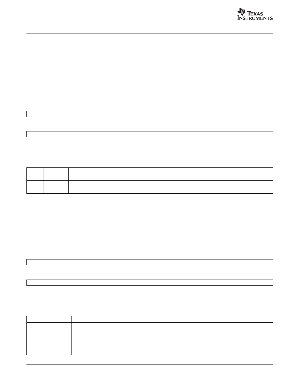
www.ti.com
VLYNQ Port Registers
3.17 Chip Version Register (CHIPVER)
VLYNQ allows inter-connection of many VLYNQ devices. In order for software to control the device
functions, there must be a mechanism that allows the software to identify VLYNQ devices. Each device
that has a VLYNQ module in it has a unique device ID associated with it, which is software readable via a
memory-mapped register within the VLYNQ module called the chip version register (CHIPVER). This is
also useful in communicating with remote devices, as the local VLYNQ device register map contains a
copy of the remote device's registers as well. This allows the software to determine the remote chip ID
and, hence, determine the remote memory-map without trying to access random remote addresses to find
a device ID register. The CHIPVER is shown in Figure 25 and described in Table 23 .
Figure 25. Chip Version Register (CHIPVER)
31 16
DEVREV
R-0
15 0
DEVID
R-25h
LEGEND: R = Read only; - n = value after reset
Table 23. Chip Version Register (CHIPVER) Field Descriptions
Bit Field Value Description
31-16 DEVREV 0-FFFFh Device revision. This field reflects the value of the device revision pins.
15-0 DEVID 0-FFFFh Device ID.
25h DM644x device ID.
3.18 Auto Negotiation Register (AUTNGO)
The auto negotiation register (AUTNGO) reflects the ability of the VLYNQ module residing in the device to
communicate with the remote VLYNQ device on their respective abilities after reset. The AUTNGO is
shown in Figure 26 and described in Table 24 .
Figure 26. Auto Negotiation Register (AUTNGO)
31 17 16
Reserved 2X
R-0 R-0
15 0
Reserved
R-0
LEGEND: R/W = Read/Write; R = Read only; - n = value after reset
Table 24. Auto Negotiation Register (AUTNGO) Field Descriptions
Bit Field Value Description
31-17 Reserved 0 Reserved. Always read as 0. Writes have no effect.
16 2X Version 2.x mode.
0 Indicates that a link was established with a remote device that has a version 1.x VLYNQ module in it.
1 Indicates that a link was established with a remote device that has a version 2.x VLYNQ module in it.
15-0 Reserved 0 Reserved. Always read as 0. Writes have no effect.
VLYNQ Port38 SPRUE36A – September 2007
Submit Documentation Feedback
Page 39

www.ti.com
4 Remote Configuration Registers
The remote configuration registers listed in Table 25 are the same registers as previously described, but
they are for the remote VLYNQ device.
Note: Before attempting to access the remote registers (offsets 80h through C0h) , you must
ensure that a link is established with the remote device. Poll the LINK bit in the VLYNQ
status register (STAT) to do this.
It is not necessary to configure the address translation registers to access the remote
device's memory-mapped registers after the link has been established.
Depending on the version and chip specific implementation, the VLYNQ module on the
remote device might have additional registers or different reset values. Refer to the remote
device data sheet for a precise description of the VLYNQ registers that exist in the remote
device.
Offset Acronym Register Description
80h RREVID Remote Revision Register
84h RCTRL Remote Control Register
88h RSTAT Remote Status Register
8Ch RINTPRI Remote Interrupt Priority Vector Status/Clear Register
90h RINTSTATCLR Remote Interrupt Status/Clear Register
94h RINTPENDSET Remote Interrupt Pending/Set Register
98h RINTPTR Remote Interrupt Pointer Register
9Ch RXAM Remote Transmit Address Map Register
A0h RRAMS1 Remote Receive Address Map Size 1 Register
A4h RRAMO1 Remote Receive Address Map Offset 1 Register
A8h RRAMS2 Remote Receive Address Map Size 2 Register
ACh RRAMO2 Remote Receive Address Map Offset 2 Register
B0h RRAMS3 Remote Receive Address Map Size 3 Register
B4h RRAMO3 Remote Receive Address Map Offset 3 Register
B8h RRAMS4 Remote Receive Address Map Size 4 Register
BCh RRAMO4 Remote Receive Address Map Offset 4 Register
C0h RCHIPVER Remote Chip Version Register
C4h RAUTNGO Remote Auto Negotiation Register
C8h RMANNGO Remote Manual Negotiation Register
CCh RNGOSTAT Remote Negotiation Status Register
E0h RINTVEC0 Remote Interrupt Vector 3-0 Register
E4h RINTVEC1 Remote Interrupt Vector 7-4 Register
Remote Configuration Registers
Table 25. VLYNQ Port Remote Controller Registers
SPRUE36A – September 2007 VLYNQ Port 39
Submit Documentation Feedback
Page 40

www.ti.com
Appendix A
Appendix A VLYNQ Protocol Specifications
VLYNQ relies on 8b/10b block coding to minimize the number of serial pins and allow for in-band
packet delineation and control. The following sections include general 8b/10b coding definitions and
their implementation.
A.1 Special 8b/10b Code Groups
Code Group Name Octet Value Octet Bits Current RD - Current RD +
K28.0 1C 0001 1100 001111 0100 110000 1011
K28.1 3C 0011 1100 001111 1001 110000 0110
K28.2 5C 0101 1100 001111 0101 110000 1010
K28.3 7C 0111 1100 001111 0011 110000 1100
K28.4 9C 1001 1100 001111 0010 110000 1101
K28.5 BC 1011 1100 001111 1010 110000 0101
K28.6 DC 1101 1100 001111 0110 110000 1001
K28.7 FC 1111 1100 001111 1000 110000 0111
K23.7 F7 1111 0111 111010 1000 000101 0111
K27.7 FB 1111 1011 110110 1000 001001 0111
K29.7 FD 1111 1101 101110 1000 010001 0111
K30.7 FE 1111 1110 011110 1000 100001 0111
Table A-1. Special 8b/10b Code Groups
A.2 Supported Ordered Sets
Each VLYNQ module must support a limited number of ordered sets. Ordered sets provide for the
delineation of packets and synchronization between VLYNQ modules at opposite ends of the serial
connection. VLYNQ 2.0 and later versions do not require some of the following ordered sets.
Code Ordered Set Encoding Octet Value
/I/ Idle /K28.5/ BC
/T/ End of Packet /K29.7/ FD
/M/ Byte Disable /K23.7/ F7
/P/ Flow Control Enable /K28.0/ IC
/C/ Flow Control Disable /K28.2/ 5C
/E/ Error Indication /K28.1/ 3C
/0/ Init0 /K28.4/ 9C
/I/ Init1 /K28.6/ DC
/L/ Link /K30.7/ FE
Table A-2. Supported Ordered Sets
40 VLYNQ Protocol Specifications SPRUE36A – September 2007
Submit Documentation Feedback
Page 41

www.ti.com
A.2.1 Idle (/I/)
bytecnt
10bits
cmd2
10bits
cmd1
10bits
address
<4*10bits
data
N*10bits
eop
10bits
pkttype adrmask
The idle ordered sets are transmitted continuously and repetitively whenever the serial interface is idle.
Idle is also used in the place of the flowed code in VLYNQ versions 2.0 and later.
A.2.2 End of Packet (/T/)
An end of packet delimiter delineates the ending boundary of a packet.
A.2.3 Byte Disable (/M/)
The byte disable symbol masks bytes for write operations.
A.2.4 Flow Control Enable (/P/)
A flow control enable request is transmitted when a VLYNQ module’s receive FIFO is full or nearly full.
This code causes the remote VLYNQ device to cease transmission of data.
A.2.5 Flow Control Disable (/C/)
The flow control disable request is transmitted by a VLYNQ module when RX FIFO resources are
available to accommodate additional data.
A.2.6 Error Indication (/E/)
The error indication is transmitted when errors are detected within a packet. Examples of such errors
include illegal packet types and code groups.
VLYNQ 2.0 Packet Format
A.2.7 Init0 (/0/)
The Init0 code group is used during the link initialization sequence. VLYNQ 2.0 and later versions use this
code with an extra byte for identifying version 1.X devices.
A.2.8 Init1 (/1/)
The Init1code group is used during the Link initialization sequence. VLYNQ 2.0 and later uses this code
with an extra byte for identifying version 1.X devices.
A.2.9 Link (/L/)
The link code group is used during the link initialization sequence. A link code group is also transmitted
each time the internal link timer expires.
A.3 VLYNQ 2.0 Packet Format
The VLYNQ 2.0 packet format is shown in Figure A-1 and described in Table A-3 , where 0<N<65.
Multi-byte fields are transferred least-significant byte first.
Figure A-1. Packet Format (10-bit Symbol Representation)
SPRUE36A – September 2007 VLYNQ Protocol Specifications 41
Submit Documentation Feedback
Page 42

www.ti.com
VLYNQ 2.0 Packet Format
Field Value Description
PKTTYPE[3:0] This field indicates the packet type.
ADRMASK[3:0] Indicates which byte of the address is included in the packet. Only address bytes that have changed
BYTECNT[7:0] Byte count. This field indicates the total number of bytes in the packet. This field is only included for
ADDRESS[7:0] Address byte 0. This byte is included only if ADRMASK[0] is set to 1. If ADRMASK[0] is cleared to 0,
ADDRESS[15:8] Address byte 1. This byte is included only if ADRMASK[1] is set to 1. If ADRMASK[1] is cleared to 0,
ADDRESS[23:16] Address byte 2. This byte is only included if ADRMASK[2] is set to 1. If ADRMASK[2] is cleared to 0,
ADDRESS[31:24] Address byte 3. This byte is only included if ADRMASK[3] is set to 1. If ADRMASK[3] is cleared to 0,
DATA Data payload. The maximum data payload size is limited to sixteen 32-bit words to allow it to fit in the
EOP End of packet indicator, /T/.
Table A-3. Packet Format (10-bit Symbol Representation) Description
0000 Reserved
0001 Write with address increment.
0010 Reserved
0011 Write 32-bit word with address increment.
0100 Reserved
0101 Configuration write with address increment.
0110 Reserved for extended command indicator (cmd2).
0111 Interrupt
1000 Reserved
1001 Read with address increment.
1010 Reserved
1011 Read 32-bit word with address increment.
1100 Reserved
1101 Configuration read with address increment.
1110 Reserved for VLYNQ version 2.0 and later.
1111 Read response for all VLYNQ versions.
since the previous address will be included. Each bit corresponds to one byte of address.
write, read, and configuration packet types. All other packet types have fixed lengths and do not
require this field.
assume this byte is equal to bits 7:0 of the previous address. Read response packets do not include
this field.
assume this byte is equal to bits 15:8 of the previous address. Read response packets do not include
this field.
this assume this byte is equal to bits 23:16 of the previous address. Read response packets do not
include this field.
assume this byte is equal to bits 31:24 of the previous address. Read response packets do not
include this field.
RX FIFO.
The CMD2 bit is only included in the packet, if the packet type indicates extended command
(PKTTYPE = 0110).
Use configuration packet types to remotely access VLYNQ module registers. The configuration packet
types do not depend on control register bit settings.
VLYNQ Protocol Specifications42 SPRUE36A – September 2007
Submit Documentation Feedback
Page 43

www.ti.com
A.4 VLYNQ 2.X Packets
An example of what can happen to a write burst due to remote and local FIFO state changes and the link
pulse timer expiring is shown in Example A-1 . This protocol can be extended to apply to multiple channels;
therefore, the data return channel is logically isolated from the command channel.
Example A-1. A write burst due to remote and local FIFO state changes and the link pulse timer
expiring
Basic packets:
Read32 - caaaaT
Write32 - caaaaddddT
ReadCfg - claaaaT
WriteCfg - claaaadddd ddddT
ReadBurst - claaaaT
WriteBurst - claaaadddddddd ddddT
Int - cddddT
ReadReturn - cldddd ddddT
Where
I - Idle
VLYNQ 2.X Packets
T - EndOfPacket
d - data
a - address
c - command
l - length
M - Byte mask
I[#] - Flowed, # is used when exiting flowed for a channel, the # is actually the current
channel command.
P# - Flow Enable for a channel
C# - Flow Disable for a channel
L - Link pulse
and what is in italics is optional data up to 16 words total.
Packet with byte enables:
WriteBurst - claaaaMMddMMdd MMddT
The above packet wrote to the LS half words from the specified address.
Packet that has been flowed due to remote FIFO status:
WriteBurst - claaaaMMddM IIIIIIIIIIIII#Mdd MMddT
The packet was extended using the I code. The # is used to
indicate that the same channel was continued.
To the same packet, the potential flowing of the local FIFO’s is added:
WriteBurst - claaaaMMddMIIP# IIIIIIIIIIIII#Mdd MMdC# dT
Link pulse to the stream is added:
WriteBurst - claaLaaMMddMIIP# IIIIIIIIIII#Mdd MMdC# dT
An example of a write burst flowed and interrupted by a read return data burst is shown below. In the
example, a 1 indicates a data return channel (it is actually the return data command) and a 0 indicates a
command channel, which is the command for the transaction.
IIIIclaaaadddd Iclddd III1dddd II0ddddddddddddd IIIIII0dddT IIIII1dT IIII
SPRUE36A – September 2007 VLYNQ Protocol Specifications 43
Submit Documentation Feedback
Page 44

www.ti.com
VLYNQ 2.X Packets
A command, length, address, and start receive data from the idle stream. A flow enable was received for
the command channel, but there is data to return, so the flow is followed by a channel 1 descriptor (the
command for return data actually indicates a channel 1), and the channel 1 packet is now under way. A
flow is now received for channel 1, but it is soon disabled so the channel 1 packet continues. The flow is
enabled for channel one again, quickly after flow is released for channel 0, so the data continues for
channel 0 when a flow is received again for channel 0. Channel 0 then receives a flow disable, completes
its packet, followed by channel 1 flow disable, where the channel 1 packet is also completed.
44 VLYNQ Protocol Specifications SPRUE36A – September 2007
Submit Documentation Feedback
Page 45

www.ti.com
Appendix B Write/Read Performance
B.1 Write Performance
The max write rate describes the maximum available data rate of the serial interface for transmission,
taking into consideration the 8b/10b encoding overheads. This is calculated as follows:
Max write rate = VLYNQ Serial Clock (MHZ) × No. of Pins × 8b/10b encoding overhead
The 8b/10b encoding overhead essentially accounts for 20% overhead, thus the actual data throughput
after subtraction of the encoding overhead gives a factor of 0.8. For example, if the VLYNQ clock is
running at 99 MHZ on a 4 pin per direction interface, the raw data is 99 × 4 or 396 Mbps. After the 8B10B
encoding is removed, the maximum write rate is 396 × 0.8 = 316.8 Mbps.
The total throughput on the VLYNQ interface includes both transmit and receive directions. Therefore, for
the above configuration, a remote device can also be writing to the local device at the same data rates,
then the total throughput is the sum of transmit and receive rates, or 633.6 Mbps.
In addition to the 8b/10b encoding, the packet structure for read/write operations also results in additional
overheads. The VLYNQ module can transfer single 32-bit words or a burst of up to sixteen 32-bit words.
The packet structure of the writes is shown below, here each character represents a byte.
Appendix B
The following sections discuss the write versus read performance and how the throughput (read or
write) should be calculated for a given data width and serial clock frequency.
Note: The data and throughput calculations shown here are sample calculations for most
ideal situations. In general, the data rates depend on a variety of other factors, such
as efficiency of read/write burst transactions, ability of buffering up read/write data,
and how best it can be serially shifted out without stalling additional read/write data
burst, remote and local components , both external and internal (device operations,
board considerations, etc.).
Write32 - caaaaddddT
WriteBurst - claaaadddddddd ddddT
Where
T - EndOfPacket
d - data, dddd represents additional 32-bit words in burst, up to 16 words.
a - address
c - command
l - length
The example above illustrates that single writes require 6 bytes of overhead, while burst writes require
8 bytes of overhead (due to the additional length of the field). From this, a scaling factor can be calculated
(data bytes/total bytes), as show in Table B-1 . The actual throughput is then calculated as the [scaling
factor] × [max write rate].
Table B-2 compares the throughput using a VLYNQ interface running at 76.5 MHZ and 99 MHZ.
SPRUE36A – September 2007 Write/Read Performance 45
Submit Documentation Feedback
Page 46

www.ti.com
Write Performance
Table B-1. Scaling Factors
Burst Size in 32-bit words Data Bytes Overhead Bytes Scaling Factor
1 4 6 40%
4 16 7 69.56%
8 32 7 82.05%
16 64 7 90.14%
Table B-2. Expected Throughput (VLYNQ Interface Running at 76.5 MHZ and 99 MHZ)
Number of VLYNQ Pins 32-bit Words Mbits/sec Mbytes/sec Mbits/sec Mbytes/sec
Burst Size in
1 1 24.19 3.02 31.68 3.96
4 42.07 5.26 55.09 6.89
8 49.62 6.20 64.98 8.12
16 54.52 6.81 71.39 8.92
2 1 48.38 6.05 63.36 7.92
4 84.14 10.52 110.18 13.77
8 99.25 12.41 129.97 16.25
16 109.03 13.63 142.78 17.85
3 1 72.58 9.07 95.04 11.88
4 126.21 15.78 165.27 20.66
8 148.87 18.61 194.95 24.37
16 163.55 20.44 214.17 26.77
4 1 96.77 12.10 126.72 15.84
4 168.28 21.03 220.37 27.55
8 198.50 24.81 259.93 32.49
16 218.07 27.26 285.56 35.70
Interface Running at 76.5 MHZ Interface Running at 99 MHZ
46 Write/Read Performance SPRUE36A – September 2007
Submit Documentation Feedback
Page 47

www.ti.com
Read Performance
B.2 Read Performance
Since reads must complete a transmit-remote read-receive cycle before starting another read transaction,
the data throughput is lower as compared to writes. There is latency involved in reading the data from the
remote device; and in some cases, a local latency in writing the returned data before the next read can
start.
The max read rate is calculated the same way as the max write rate. The packet overhead is as shown
below:
Read32 - caaaaT
ReadBurst - claaaaT
ReadReturn - cldddd ddddT
Where
T - EndOfPacket
d - data, dddd represents additional 32-bit words in burst, up to 16 words.
a - address
c - command
l - length
There are 6 bytes of overhead for a single read, 7 bytes for burst reads, and 3 bytes for read returns. The
time required for a read is the total of the time for the read request, remote latency, read return, and local
latency. Thus, the throughput can be calculated as data bytes/total transaction time, where the latency of
both local and remote devices is combined.
Read Throughput = data/ (((Read + ReadReturn + data)/max read rate) + Latency
For example, with a 4 pin, 99 MHZ VLYNQ connection, for a single 32-bit word read:
Read Throughput = 32 bits × 316.8 Mbps/ (6 × 8 + 3 × 8 + 4 × 8 + Latency × 316.8 Mbps)
Similarly, for a burst read of sixteen 32-bit words, with a 4 pin, 99 MHZ VLYNQ connection
Read Throughput = 16 × 32 bits × 316.8Mbps/(6 × 8 + 3 × 8 + 16 × 4 × 8 + Latency × 316.8 Mbps)
Using the formula above, the relative performance with various latencies is illustrated for a 4 pin, 99 MHZ
VLYNQ clock, burst read (sixteen 32-bit words) throughput rate, as shown in Table B-3 :
= (data × max read rate)/((Read + ReadReturn + data) + Latency × max
read rate)
= 10137.6/(104 + Latency × 316.8 Mbps)
= 162201.6/(584 + Latency × 316.8 Mbps)
Table B-3. Relative Performance with Various Latencies
Number of VLYNQ Pins Throughput Throughput
(99 MHZ) Burst Size in 32-bit Words Latency ( μ sec) (Mbits/sec) (Mbytes/sec)
4 16 0 277.74 34.72
1 179.70 22.46
10 43.02 5.38
100 5.00 0.62
To efficiently use VLYNQ bandwidth, it is desirable for each VLYNQ device to write from the local device
to the remote device. Burst transactions are more efficient than single read/write transactions.
SPRUE36A – September 2007 Write/Read Performance 47
Submit Documentation Feedback
Page 48

www.ti.com
Appendix C
Appendix C Revision History
Table C-1 lists the changes made since the previous version of this document.
Reference Additions/Modifications/Deletions
Section 2.9 Changed fourth paragraph.
Table 8 Changed Description of INTLOCAL.
Section 3.17 Changed paragraph.
Figure 25 Changed DEVID reset value.
Table 23 Changed DEVID Description.
Figure A-1 Changed figure.
Table A-3 Changed Description of PKTTYPE[3:0] = 0110.
Table B-2 Changed table.
Table C-1. Document Revision History
Added NOTE.
Deleted Table B-3. Subsequent tables renumbered.
48 Revision History SPRUE36A – September 2007
Submit Documentation Feedback
Page 49

IMPORTANT NOTICE
Texas Instruments Incorporated and its subsidiaries (TI) reserve the right to make corrections, modifications, enhancements,
improvements, and other changes to its products and services at any time and to discontinue any product or service without notice.
Customers should obtain the latest relevant information before placing orders and should verify that such information is current and
complete. All products are sold subject to TI’s terms and conditions of sale supplied at the time of order acknowledgment.
TI warrants performance of its hardware products to the specifications applicable at the time of sale in accordance with TI’s
standard warranty. Testing and other quality control techniques are used to the extent TI deems necessary to support this
warranty. Except where mandated by government requirements, testing of all parameters of each product is not necessarily
performed.
TI assumes no liability for applications assistance or customer product design. Customers are responsible for their products and
applications using TI components. To minimize the risks associated with customer products and applications, customers should
provide adequate design and operating safeguards.
TI does not warrant or represent that any license, either express or implied, is granted under any TI patent right, copyright, mask
work right, or other TI intellectual property right relating to any combination, machine, or process in which TI products or services
are used. Information published by TI regarding third-party products or services does not constitute a license from TI to use such
products or services or a warranty or endorsement thereof. Use of such information may require a license from a third party under
the patents or other intellectual property of the third party, or a license from TI under the patents or other intellectual property of TI.
Reproduction of TI information in TI data books or data sheets is permissible only if reproduction is without alteration and is
accompanied by all associated warranties, conditions, limitations, and notices. Reproduction of this information with alteration is an
unfair and deceptive business practice. TI is not responsible or liable for such altered documentation. Information of third parties
may be subject to additional restrictions.
Resale of TI products or services with statements different from or beyond the parameters stated by TI for that product or service
voids all express and any implied warranties for the associated TI product or service and is an unfair and deceptive business
practice. TI is not responsible or liable for any such statements.
TI products are not authorized for use in safety-critical applications (such as life support) where a failure of the TI product would
reasonably be expected to cause severe personal injury or death, unless officers of the parties have executed an agreement
specifically governing such use. Buyers represent that they have all necessary expertise in the safety and regulatory ramifications
of their applications, and acknowledge and agree that they are solely responsible for all legal, regulatory and safety-related
requirements concerning their products and any use of TI products in such safety-critical applications, notwithstanding any
applications-related information or support that may be provided by TI. Further, Buyers must fully indemnify TI and its
representatives against any damages arising out of the use of TI products in such safety-critical applications.
TI products are neither designed nor intended for use in military/aerospace applications or environments unless the TI products are
specifically designated by TI as military-grade or "enhanced plastic." Only products designated by TI as military-grade meet military
specifications. Buyers acknowledge and agree that any such use of TI products which TI has not designated as military-grade is
solely at the Buyer's risk, and that they are solely responsible for compliance with all legal and regulatory requirements in
connection with such use.
TI products are neither designed nor intended for use in automotive applications or environments unless the specific TI products
are designated by TI as compliant with ISO/TS 16949 requirements. Buyers acknowledge and agree that, if they use any
non-designated products in automotive applications, TI will not be responsible for any failure to meet such requirements.
Following are URLs where you can obtain information on other Texas Instruments products and application solutions:
Products Applications
Amplifiers amplifier.ti.com Audio www.ti.com/audio
Data Converters dataconverter.ti.com Automotive www.ti.com/automotive
DSP dsp.ti.com Broadband www.ti.com/broadband
Interface interface.ti.com Digital Control www.ti.com/digitalcontrol
Logic logic.ti.com Military www.ti.com/military
Power Mgmt power.ti.com Optical Networking www.ti.com/opticalnetwork
Microcontrollers microcontroller.ti.com Security www.ti.com/security
RFID www.ti-rfid.com Telephony www.ti.com/telephony
Low Power www.ti.com/lpw Video & Imaging www.ti.com/video
Wireless
Wireless www.ti.com/wireless
Mailing Address: Texas Instruments, Post Office Box 655303, Dallas, Texas 75265
Copyright © 2007, Texas Instruments Incorporated
 Loading...