

Page 1
User's Guide
SLOU352–November 2012
VCA5807 Development Guide
This development guide describes the characteristics, operation and use of the VCA5807EVM
demonstration kit. This demonstration kit is an evaluation module for the VCA5807 device. The VCA5807
is an integrated Voltage Controlled Amplifier (VCA) that integrates a complete time-gain-control (TGC)
imaging path and a continuous wave Doppler (CWD) path. The VCA5807 is intended for prototyping and
evaluation. This user's guide includes a complete circuit description, schematic diagram, and bill of
materials (BOM).
The following related documents are available through the Texas Instruments web site at
http://www.ti.com.
Table 1. Related Document
Device Literature Number
VCA5807 SLOS727
Contents
1 VCA5807 Overview ......................................................................................................... 3
1.1 Important Disclaimer Information ................................................................................ 3
2 Overview ..................................................................................................................... 3
2.1 Introduction ......................................................................................................... 3
2.2 Default Configuration .............................................................................................. 4
3 Software Installation and Operation ...................................................................................... 5
3.1 Minimum Requirements ........................................................................................... 5
3.2 Installing the Software (PC Application) ........................................................................ 5
3.3 GUI Overview ....................................................................................................... 6
4 Hardware ................................................................................................................... 11
4.1 Introduction ........................................................................................................ 11
4.2 Board Configuration .............................................................................................. 12
4.3 Power .............................................................................................................. 13
4.4 Clock Buffer ....................................................................................................... 13
4.5 VCA Inputs ........................................................................................................ 13
4.6 VCA5807 Device ................................................................................................. 13
4.7 VCA Outputs ...................................................................................................... 13
4.8 CW Mode .......................................................................................................... 14
4.9 VControl ........................................................................................................... 16
4.10 Serial Interface .................................................................................................... 16
5 Quick Start .................................................................................................................. 17
5.1 Test Setup ......................................................................................................... 17
5.2 Power Up VCA5807EVM ........................................................................................ 17
5.3 Launch the VCA5807 GUI ....................................................................................... 17
Appendix A Bill of Materials (BOM) ........................................................................................... 18
Appendix B PCB Layout and Schematics ................................................................................... 22
List of Figures
1 VCA5807EVM Basic Configuration....................................................................................... 4
Pentium, Celeron are registered trademarks of Intel.
Windows is a registered trademark of Microsoft Corporation.
SLOU352–November 2012 VCA5807 Development Guide
Submit Documentation Feedback
Copyright © 2012, Texas Instruments Incorporated
1
Page 2

www.ti.com
2 Introduction Tab of the VCA5807EVM GUI ............................................................................. 6
3 Hardware/Power/RST Tab of the VCA5807EVM GUI ................................................................. 7
4 VCA LNA+VCA+PGA+LPF Tab of the VCA5807EVM GUI........................................................... 8
5 VCA CW Mode Tab......................................................................................................... 9
6 VCA Debugging/Recording Tab......................................................................................... 10
7 HW Setup................................................................................................................... 11
8 PCB Layout With Jumper Positions..................................................................................... 12
9 CW Mode Hardware Configuration...................................................................................... 14
10 Switching to CW Mode ................................................................................................... 15
11 Oscilloscope................................................................................................................ 16
12 Top Layer - Signal......................................................................................................... 22
13 Second Layer - Ground................................................................................................... 23
14 Third Layer - Power....................................................................................................... 24
15 Fourth Layer - Signal...................................................................................................... 25
16 Fifth Layer - Ground....................................................................................................... 26
17 Bottom Layer - Signal..................................................................................................... 27
18 Schematic 1 of 10 ......................................................................................................... 28
19 Schematic 2 of 10 ......................................................................................................... 29
20 Schematic 3 of 10 ......................................................................................................... 30
21 Schematic 4 of 10 ......................................................................................................... 31
22 Schematic 5 of 10 ......................................................................................................... 32
23 Schematic 6 of 10 ......................................................................................................... 33
24 Schematic 7 of 10 ......................................................................................................... 34
25 Schematic 8 of 10 ......................................................................................................... 35
26 Schematic 9 of 10 ......................................................................................................... 36
27 Schematic 10 of 10........................................................................................................ 37
List of Tables
1 Related Document.......................................................................................................... 1
2 Power Table................................................................................................................ 13
3 Bill of Materials............................................................................................................. 18
2
VCA5807 Development Guide SLOU352–November 2012
Copyright © 2012, Texas Instruments Incorporated
Submit Documentation Feedback
Page 3
www.ti.com
1 VCA5807 Overview
1.1 Important Disclaimer Information
The VCA5807EVM is intended for feasibility and evaluation testing only in
laboratory and development environments. This product is not for diagnostic
use.
Use the VCA5807 only under the following conditions:
• The VCA5807EVM is intended only for electrical evaluation of the features of the VCA5807 device in a
laboratory, simulation, or development environment.
• The VCA5807EVM is not intended for direct interface with a patient, or patient diagnostics.
• The VCA5807EVM is intended only for development purposes. It is not intended to be used as all or
part of an end-equipment application.
• The VCA5807EVM should be used only by qualified engineers and technicians who are familiar with
the risks associated with handling electrical and mechanical components, systems, and subsystems.
• The user is responsible for the safety of themself, fellow employees, contractors, and coworkers when
using or handling the VCA5807EVM. Furthermore, the user is fully responsible for the contact interface
between the human body and electronics; consequently, the user is responsible for preventing
electrical hazards such as shock, electrostatic discharge, and electrical overstress of electric circuit
components.
VCA5807 Overview
CAUTION
2 Overview
2.1 Introduction
This document is intended as a step-by-step guide through the VCA5807 Evaluation Module (EVM) setup
and test. The EVM is shipped with a default configuration from the manufacturer. With this configuration,
the onboard CMOS clock is used for an analog-to-digital converter sampling clock; the onboard oscillator
is used for CW mode operation. No external clock generator is required. The input signal for measurement
from a signal generator must be provided.
A detailed explanation regarding the jumpers, connectors, and test points appears in Section 2.2. The
graphical user interface (GUI) is available from the TI Web Site. Go to the software section of the product
folder (VCA5807).
Throughout this document, the abbreviation EVM and the term evaluation module are synonymous with
the VCA5807EVM.
SLOU352–November 2012 VCA5807 Development Guide
Submit Documentation Feedback
Copyright © 2012, Texas Instruments Incorporated
3
Page 4
Overview
2.2 Default Configuration
Figure 1 shows the default configuration of the EVM from the factory. The accompanying list identifies the
basic components on the EVM board.
www.ti.com
Figure 1. VCA5807EVM Basic Configuration
1. P1 – Power supplies connector
2. JP2, and JP3 are set to enable 3.3-V and 5-V power supplies to the device
3. JP15: Enables onboard VCNT
4. P17: Disables PDB_Global
5. P15: Chooses the device Common Mode for the I/V Amp Common Mode
6. P16: Chooses Vss as –5 V for low-side power supply on I/V Amp
4
VCA5807 Development Guide SLOU352–November 2012
Copyright © 2012, Texas Instruments Incorporated
Submit Documentation Feedback
Page 5

www.ti.com
3 Software Installation and Operation
3.1 Minimum Requirements
Before installing the software, verify that your PC meets the minimum requirements outlined in this
section.
3.1.1 Required Setup for VCA5807EVM GUI Software
• PC-compatible computer
• Pentium®III or Celeron®processor, 866 MHz or equivalent
• Minimum 256 MB of RAM (512 MB or greater recommended)
• Hard disk drive with at least 200 MB free space
• Windows®XP operating system with SP2, or Windows 7 operating system
• 1280 × 1024 or greater display screen resolution
• Mouse or other pointing device
• Available USB input
3.1.2 Additional Requirements for Use with Hardware
• VCA5807EVM
• USB cable
• Power supply to supply ±5 V
Software Installation and Operation
3.2 Installing the Software (PC Application)
The GUI software to evaluate the VCA5807 device is available at the Texas Instruments web site at
www.ti.com (VCA5807).
Before installing the software, make sure the VCA5807EVM is not connected to the PC. If using a
machine with Windows 7, it is recommended to have administrator rights to avoid problems during
installation.
Unzip the installer file to a temporary directory, and then double click setup.exe from the directory. The
installation creates a program menu item to execute the software.
Windows should automatically install the correct device drivers, but if there are problems installing the
device drivers please refer to this e2e post.
http://e2e.ti.com/support/other_analog/imaging_afes/f/239/p/213841/754871.aspx#754871
Follow these directions to ensure proper installation of the PC application.
SLOU352–November 2012 VCA5807 Development Guide
Submit Documentation Feedback
Copyright © 2012, Texas Instruments Incorporated
5
Page 6
Software Installation and Operation
3.3 GUI Overview
Every tab in the VCA5807EVM GUI has a software reset option available by clicking the Software Reset
button located at the bottom right of the GUI.
The VCA Introduction tab: This tab gives a block diagram of the VCA5807 device.
www.ti.com
Figure 2. Introduction Tab of the VCA5807EVM GUI
6
VCA5807 Development Guide SLOU352–November 2012
Copyright © 2012, Texas Instruments Incorporated
Submit Documentation Feedback
Page 7
www.ti.com
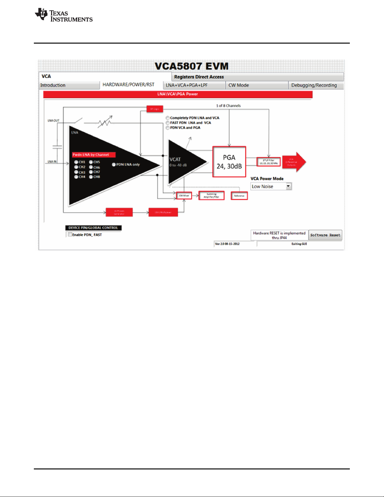
The VCA HARDWARE/POWER/RST tab: This tab allows the execution of different power down options.
Software Installation and Operation
Figure 3. Hardware/Power/RST Tab of the VCA5807EVM GUI
SLOU352–November 2012 VCA5807 Development Guide
Submit Documentation Feedback
Copyright © 2012, Texas Instruments Incorporated
7
Page 8
Software Installation and Operation
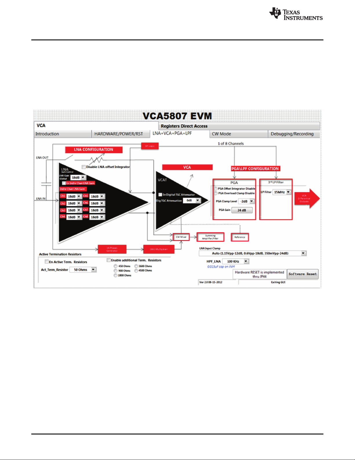
The VCA LNA+VCA+PGA+LPF tab: The settings of the Low Noise Amplifier (LNA), VCA, Programmable
Gain Amplifier (PGA), and the Low Pass Filter (LPF) are adjusted in this tab.
• LNA: Adjusts the gain of each channel, adjust the active termination resistors, and disable the LNA
offset Integrator
• VCA: Adjusts the digital Time Gain Control (TGC) Attenuator
• PGA: Adjusts the PGA gain, Clamp Level, and disable both the overload clamp and the offset
integrator
• LPF: Adjusts the LPF frequency
www.ti.com
Figure 4. VCA LNA+VCA+PGA+LPF Tab of the VCA5807EVM GUI
8
VCA5807 Development Guide SLOU352–November 2012
Copyright © 2012, Texas Instruments Incorporated
Submit Documentation Feedback
Page 9
www.ti.com
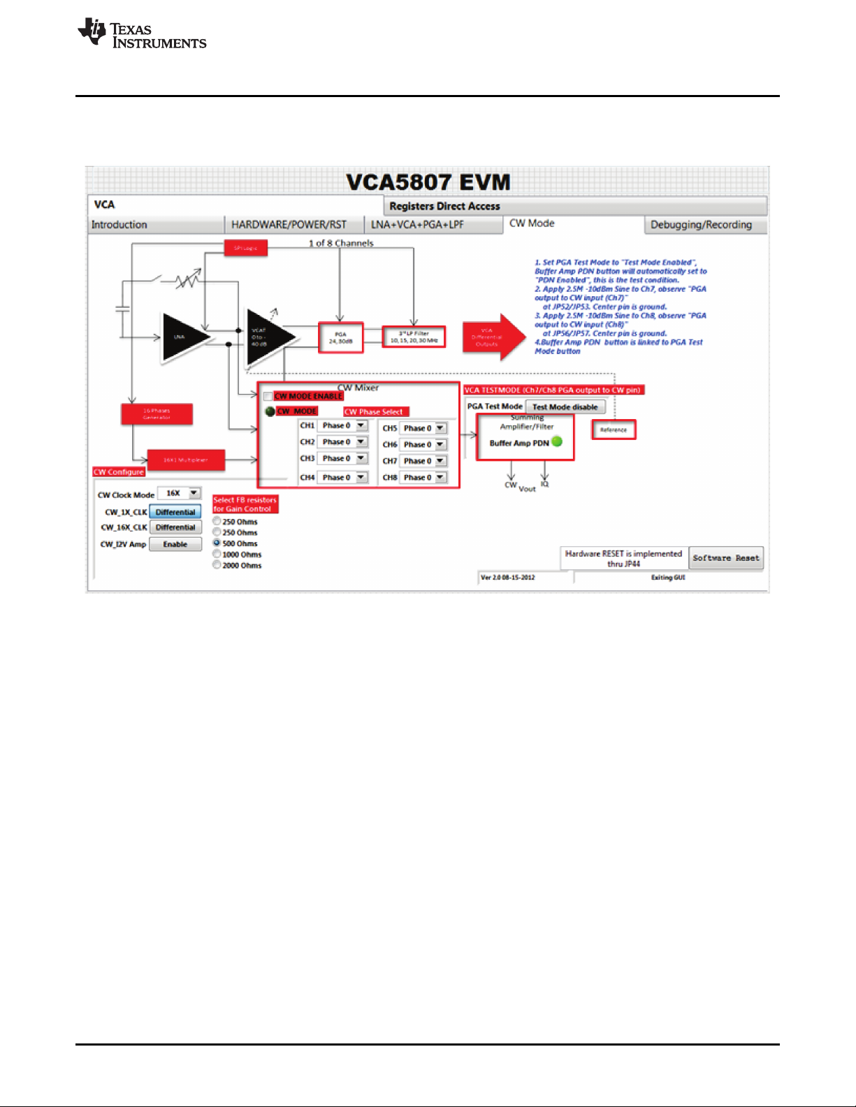
The VCA CW Mode tab: The Continuous-wave (CW) Doppler mode is adjusted in this tab as well as the
phases of each CW channel (1-8), the CW CLK, and the feedback resistors to control the gain. CH7 and
CH8 are brought to the CW pins by using the PGA Test Mode.
Software Installation and Operation
Figure 5. VCA CW Mode Tab
SLOU352–November 2012 VCA5807 Development Guide
Submit Documentation Feedback
Copyright © 2012, Texas Instruments Incorporated
9
Page 10
Software Installation and Operation
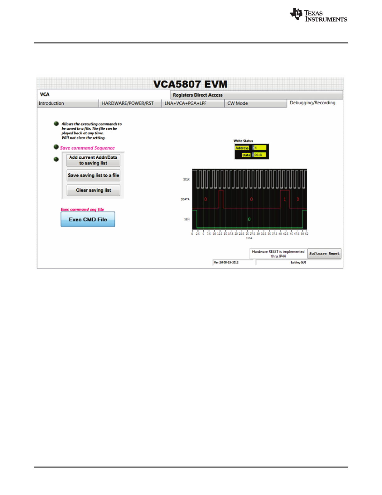
The VCA Debugging/Recording tab: Command executions are saved to a file in this tab. The file can be
played back at any time by clicking on the Exec CMD File button. This tab also displays the Write Status,
and the ability to see the digital waveform of the SCLK, SDATA, and SEN pins.
www.ti.com
Figure 6. VCA Debugging/Recording Tab
10
VCA5807 Development Guide SLOU352–November 2012
Copyright © 2012, Texas Instruments Incorporated
Submit Documentation Feedback
Page 11
www.ti.com
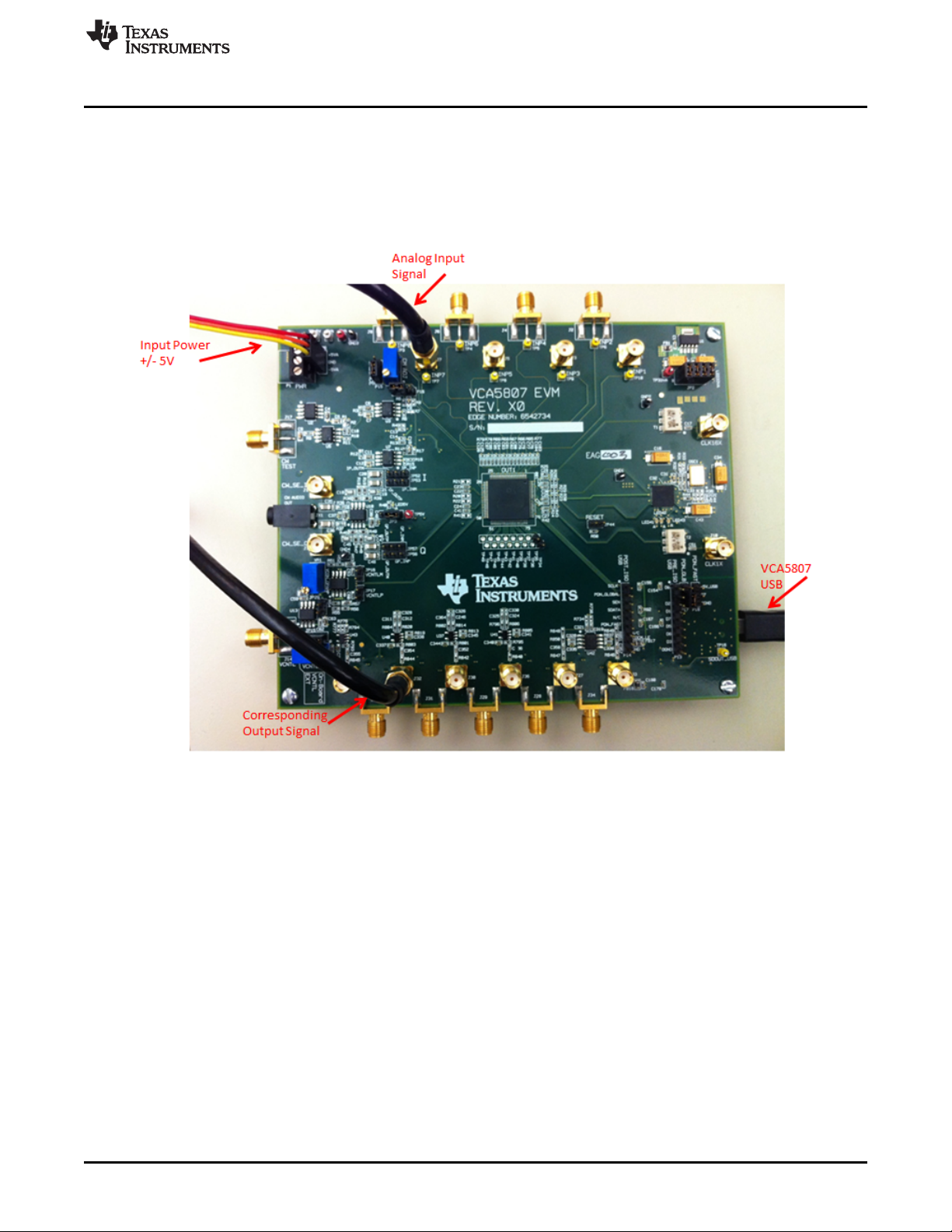
4 Hardware
4.1 Introduction
The following illustration shows the setup of the VCA5807EVM and external connectors. For the default
configuration as shown in Figure 1, it is unnecessary to have an external sampling clock and external
Vcntl supply. The onboard CMOS clock and onboard Vcntl are used.
Hardware
Figure 7. HW Setup
SLOU352–November 2012 VCA5807 Development Guide
Submit Documentation Feedback
Copyright © 2012, Texas Instruments Incorporated
11
Page 12
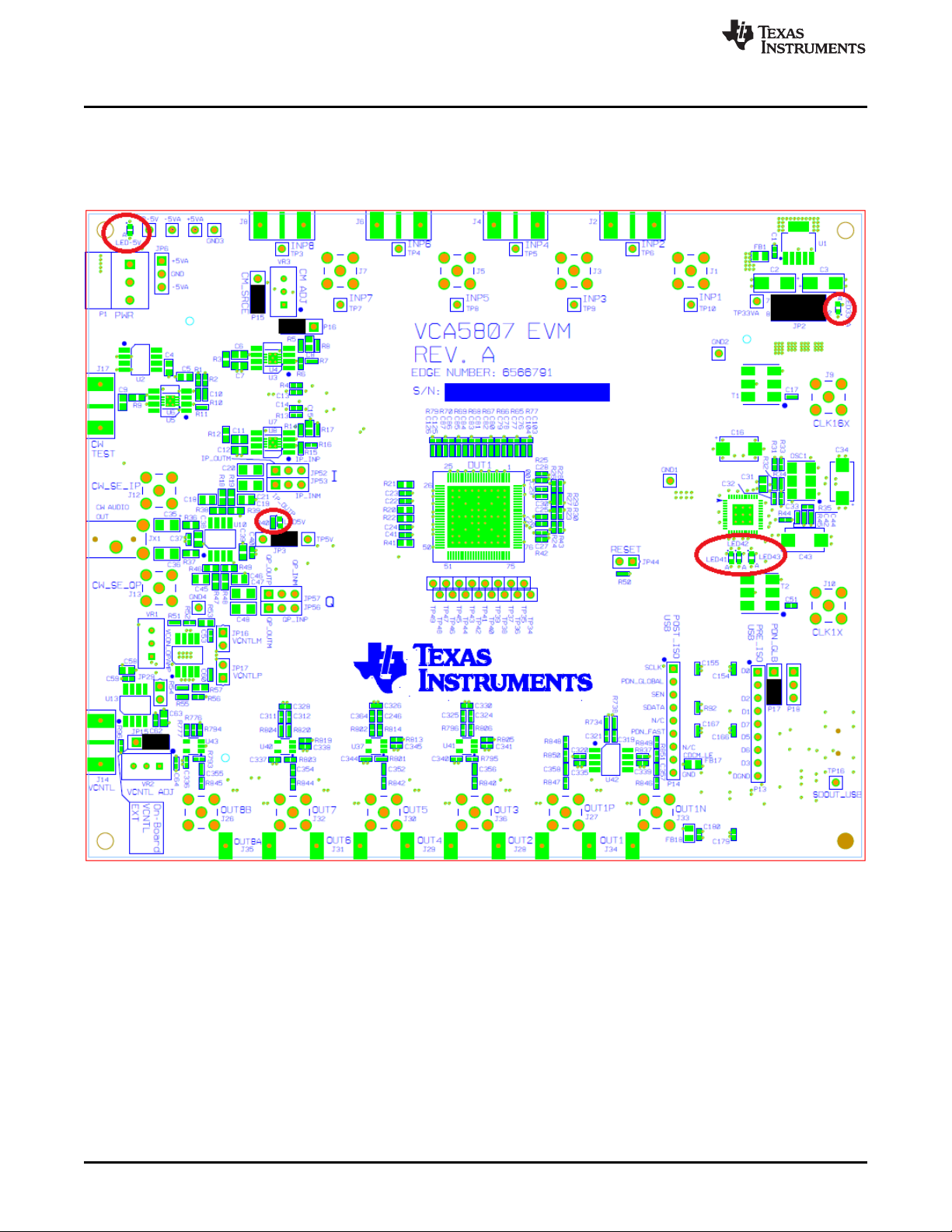
Hardware
4.2 Board Configuration
Power up the VCA5807EVM by applying +5 V and –5 V to the P1 connector. After power up is complete,
three green LEDs and three red LEDs (LED 41, LED42, and LED 43) are turned. Locations of LEDs are
shown in Figure 8.
www.ti.com
12
Figure 8. PCB Layout With Jumper Positions
VCA5807 Development Guide SLOU352–November 2012
Copyright © 2012, Texas Instruments Incorporated
Submit Documentation Feedback
Page 13

www.ti.com
4.3 Power
The power configuration of the board is shown in Figure 18, page 1 of the schematic. Refer to Table 2 for
a list of important power components.
Connector Description
P1/JP6 P1 is the +5-V and –5-V power supply connector. JP6 is the test point for +5-V/-5-V
JP3 Onboard 5-V enable. The configuration must be set up as shown in Figure 7 in order to
TP-5V -5-V supply test point
+5VA +5-V supply test point
JP2 Onboard 3.3-VA enable. The configuration must be set up as shown in Figure 7 in order
TP33VA +3.3-VA supply test point
TP1 through TP4 Ground test points
4.4 Clock Buffer
The clock buffer drives the VCA5807 device. Each clock buffer output should only drive one VCA5807. Do
not use one clock to drive multiple VCA5807s. This is due to the fact that the clock buffer's load
capacitance increases by a factor of N, which then results in degraded falling and rising times. Select
different clock inputs in the GUI. LEDs 41 and 42 demonstrate the PLL status of the clock buffer.
Hardware
Table 2. Power Table
power supply.
use onboard 5-V supply.
to use the onboard 3.3 V.
4.5 VCA Inputs
J1 through J8 are the analog input signals for CH1 through CH8. Connect to a signal generator. If the
signal is too noisy, apply a bandpass filter between the generator and the SMA to get a better result. Use
TP3-TP10 to see the input signal to the board.
4.6 VCA5807 Device
The VCA5807 device is a suitable ultrasound analog front end solution for high-end systems and portable
systems. This device contains eight channels of VCA, and CW mixer. The VCA includes an LNA, Voltagecontrolled Attenuator (VCAT), PGA, and an LPF. Each of these features is adjusted via the VCA5807
EVM GUI. For a more detailed explanation of the VCA5807 device please refer to the datasheet. The
datasheet is found on the TI product folder at www.ti.com. (SLOS727)
4.7 VCA Outputs
J26 through J36 are the output signals for CH1 through CH8. All channels have a single-ended output
through an OPA842 buffer amplifier. However, CH1 has the option of a fully differential output signal
through a THS4130 amplifier. In order to use this amplifier, install R734 and R738 and remove R837,
C317, and C318. CH8 also provides an added feature by allowing the choice of the OPA830 as the buffer
amplifier. In order to use this amplifier, install R776 and R777 and remove U35.
SLOU352–November 2012 VCA5807 Development Guide
Submit Documentation Feedback
Copyright © 2012, Texas Instruments Incorporated
13
Page 14

Hardware
4.8 CW Mode
www.ti.com
Figure 9. CW Mode Hardware Configuration
14
VCA5807 Development Guide SLOU352–November 2012
Copyright © 2012, Texas Instruments Incorporated
Submit Documentation Feedback
Page 15

www.ti.com
• Go to the CW Mode tab on the GUI.
• Check CW MODE ENABLE. LED41, LED42, and LED43 on the VCA5807EVM should all illuminate.
• Select 500 Ω for the gain control feedback resistor.
Hardware
Figure 10. Switching to CW Mode
SLOU352–November 2012 VCA5807 Development Guide
Submit Documentation Feedback
Copyright © 2012, Texas Instruments Incorporated
15
Page 16

Hardware
• Apply an analog signal (2.51 MHz, –10 dBm) to any analog input SMA.
• The CW outputs (J12, J13) display the frequency I and Q signals at 10 kHz as shown in Figure 11.
www.ti.com
The GUI Gain Control Feedback Resistor can vary the amplitude of the outputs.
4.9 VControl
Switch between using the onboard Vcntl or the external Vcntl by using JP15. External Vcntl can range
from 0 V to 1.5 V. If using the external Vcntl, then a DC voltage source must be connected to J14. The
default setup uses onboard Vcntl. VR2 is used to make onboard Vcntl adjustments.
4.10 Serial Interface
The serial interface of the board is located on the bottom right-hand side. USB1 is the USB interface
connector. P13 and P14 are test points for the USB data bus: From pin 1 to pin 9, the signals are D0, D4,
D2, D1, D7, D5, D6, D3, and DGND. P14 on the VCA5807EVM is not installed.
Figure 11. Oscilloscope
16
VCA5807 Development Guide SLOU352–November 2012
Copyright © 2012, Texas Instruments Incorporated
Submit Documentation Feedback
Page 17

www.ti.com
5 Quick Start
This section assumes all engineering knowledge on the device and basic overview of the VCA5807EVM.
5.1 Test Setup
Connect the EVM as shown in . Typical input signals are 5 MHz at –32 dBm. This can be applied to any
VCA input (J1-J8). If the signal is noisy, consider using a 5-MHz filter. Connect a scope or a spectrum
analyzer to the corresponding VCA output in order to measure the gain on the channel.
5.2 Power Up VCA5807EVM
Connect ±5-V power to the board. No other power connection is needed.
5.3 Launch the VCA5807 GUI
Launch the VCA5807EVM GUI. Execute a software reset with the GUI and verify the current consumption
drops from ≈0.762 A to ≈0.646 A. Enable the Active Termination Resistor of 50 Ohms (check the box) on
the LNA+VCA+PGA+LPF tab. This tab is also used to vary the gain on each channel. However, with the
default settings as shown in , the gain should be 42 dB overall. Therefore, with an input signal of 5 MHz at
–32 dBm, load resistance of 50 Ω, and an overall gain of 42 dB, the output should read ≈4 dBm or 1 Vpp.
For more details and other modes for testing and evaluating the VCA5807 device, please refer to the
previous pages of this development guide.
Quick Start
SLOU352–November 2012 VCA5807 Development Guide
Submit Documentation Feedback
Copyright © 2012, Texas Instruments Incorporated
17
Page 18

www.ti.com
Appendix A Bill of Materials (BOM)
This section contains Table 3, the BOM for the VCA5807EVM.
Table 3. Bill of Materials
Item Qty MFG MFG Part# REF DES Description Value or Function
1 41 AVX 0402YC104KAT2A C17, C25, C26, C29, C30, C33, C37, CAP,SMT,0402 CAPACITOR,SMT,0402,CER,16V,10
2 2 AVX 0402YC471KAT2A C53,C60 CAP,SMT,0402 CAPACITOR,SMT,0402,CER,16V,10
3 40 0402YC104KAT2A C160,C162, C163, C165, C166,
4 2 AVX 0402YC222KAT2A C10, C74 CAP,SMT,0402 CAPACITOR,SMT,0402,CER,16V,10
5 11 KEMET C0402C103K3RACTU C290, C350, C351, C352, C353, CAP,SMT,0402 CAPACITOR,SMT,0402,CER,0.01uF,
6 23 KEMET C0402C104K8PAC C1, C68, C69, C152, C291, C333, CAP,SMT,0402 CAPACITOR,SMT,0402,CER,0.1uF,1
7 2 KEMET C0402C152J5GACTU C73, C89 CAP,SMT,0402 CAPACITOR,SMT,0402,CERAMIC,1
8 8 TDK C1005X5R0J105M C77, C79, C81, C83, C85, C87, CAP,SMT,0402 CAPACITOR,SMT,0402,CER,1.0uF,6
9 2 AVX 0402ZD105KAT2A C71, C72 CAP,SMT,0402 CAPACITOR,SMT,0402,CERAMIC,1.
10 8 AVX 0402YC153KAT2A C107, C108, C109, C116, C118, CAP,SMT,0402 CAPACITOR,SMT,0402,CER,15000p
11 1 AVX 04025C102KAT2A C32 CAP,SMT,0402 CAPACITOR,SMT,0402,CER,1000pF
12 4 AVX 04025C332KAT2A C22, C23, C24, C41 CAP,SMT,0402 CAPACITOR,SMT,0402,CER,3300pF
13 2 AVX 04025A470JAT2A C175, C176 CAP,SMT,0402 CAPACITOR,SMT,0402,CER,47pF,5
14 7 AVX 06033C104JAT2A C5, C7, C8, C12, C15, C88, C90 CAP,SMT,0603 CAPACITOR,SMT,0603,CERAMIC,0.
15 7 AVX 0603YD105KAT2A C38, C39, C58, C63, C159, C161, CAP,SMT,0603 CAPACITOR,SMT,0603,CERAMIC,1.
16 1 TAIYO YUDEN AMK107BJ226MA-T C9 CAP,SMT,0603 CAPACITOR,SMT,0603,CERAMIC,2
17 1 AVX 06036D106MAT2A C4 CAP,SMT,0603 CAPACITOR,SMT,0603,CERAMIC,1
18 2 AVX 0603YD105KAT2A C75, C129 CAP,SMT,0603 CAPACITOR,SMT,0603,CERAMIC,1.
19 2 MURATA GRM188C80G475KE19 C6, C11 CAP,SMT,0603 CAPACITOR,SMT,0603,CERAMIC,4.
20 3 TAIYO YUDEN JMK107BJ106MA-T C31, C348, C349 CAP,SMT,0603 CAPACITOR,SMT,0603,CERAMIC,1
21 4 KEMET C0805C332F3GACTU C18, C19, C45, C46 CAP,SMT,0805 CAPACITOR,SMT,0805,CERAMIC,3
22 6 AVX 1206YD226KAT2A C20, C21, C35, C36, C47, C48 CAP,SMT,1206 CAPACITOR,SMT,1206,CERAMIC,2
23 4 VISHAY SPRAGE 293D226X9016D2TE3 C16, C34, C43, C128 CAP,SMT,7343 CAP,TAN,SMT, 22uF,16V,+/-10%,-
24 4 AVX TPSC226K016R0375 C2, C3, C70, C151 CAPACITOR,SMT,TA 10%, 16V, 22uF
25 14 AMPHENOL 901-144-8 J1, J3, J5, J7, J9, J10, J12, J13, J26, CONNECTOR,SMA SMA COAX STRAIGHT PCB
C40, C51, C59, C62, C64, C76, C78, %,0.1uF
C80, C82, C84, C86, C94, C95, C96,
C97, C98, C99, C101, C103, C125,
C130, C131, C132, C133, C134,
C135, C136, C137, C138, C139,
C140, C141, C154, C155
%,470pF
C167, C170, C171, C173, C174,
C177, C178, C179, C180, C246,
C265, C267, C294, C295, C308,
C309, C310, C311, C312, C313,
C314, C315, C316, C317, C318,
C319, C320, C321, C322, C323,
C324, C325, C364, C365, C366
%,2200pF
C354, C355, C356, C357, C358, 25V,10%,X7R
C363
C334, C335, C336, C337, C338, 0V,10%,X5R
C339, C340, C341, C342, C343,
C344, C345, C346, C347, C360,
C361, C362
500pF,50V,5%,C0G/NP0
C104, C126 .3V,20%,X5R
0uF,10V,20%,X5R
C119, C121, C123 F,16V,10%,X7R
,50V,10%,X7R
,50V,10%,X7R
0V,5%,NPO
1uF,25V,5%,X7R
C172 0uF,16V,10%,X5R
2uF,4V,20%,X5R
0uF,6.3V,20%,X5R
0uF,16V,10%,X5R
7uF,4V,10%,X6S ( TI-F )
0uF,6.3V,20%,X5R
300pF,25V,1%,C0G(NP0)
2uF,10V,10%,X5R
55~85C
NT
J27, J30, J32, J33, J36 CURRENT P/N IS 901-144-8RFX
18
Bill of Materials (BOM) SLOU352–November 2012
Copyright © 2012, Texas Instruments Incorporated
Submit Documentation Feedback
Page 19

www.ti.com
Appendix A
Table 3. Bill of Materials (continued)
Item Qty MFG MFG Part# REF DES Description Value or Function
26 12 STEWARD HI0805R800R-00 FB1, FB6, FB7, FB8, FB9, FB10, FERRITE FERRITE,SMT,0805,80
27 1 MOLEX 39357-0003 P1 HEADER, THRU, 3P HEADER, THRU, POWER,
28 1 SAMTEC TSW-104-07-G-D JP2 HEADER,THU HEADER,THU,8P,2X4,MALE,DUAL
29 1 PBC09SAAN P13 HEADER,THU,9P HEADER,THU,MALE,0.1LS,9P,1X9,3
30 4 TYCO ELECTRONICS 4-103239-0x2 JP16, JP17, JP29, JP44 HEADER,THU,JUMP MALE,2PIN,.100CC MAKE FROM 4-
31 11 TYCO ELECTRONICS 4-103239-0x3 JP3, JP6, JP15, JP52, JP53, JP56, HEADER,THU,JUMP MAKE FROM 4-103239-0
32 3 NATIONAL SEMI LME49990MA/NOPB U3, U5, U7 IC,SMT,8P ULTRA LOW DISTORTION ULTRA
33 1 TI THS4130CD U42 IC,SMT,8P HI-SPEED,LOW NOISE,FULL-
34
35 1 TEXAS INSTRUMENTS CDCM7005RGZ CLK_BUF IC,SMT,QFN-48 3.3-V HIGH PERFORMANCE
36 3 TI ISO7240MDW U16, U20, U21 IC,SMT,SOIC-16W QUADDIGITAL ISOLATORS
37 1 TI / BURR-BROWN OPA211AID U13 IC,SMT,SOIC-8 1.1nV/Hz NOISE LOW POWER
38 1 TI OPA2614ID U10 IC,SMT,SOIC-8 DUAL HI GAIN BWIDTH HI OUTPUT
39 1 BURR-BROWN / TI REF5025AID U2 IC,SMT,SOIC-8 LOW-NOISE VERY LOW DRIFT
40 2 TI THS4131ID U15, VCON_OPAMP IC,SMT,SOIC-8 HIGH-SPEED LOW NOISE
41 1 TI TPS79633DCQR U1 IC,SMT,SOT223-6 ULTRALOW-NOISE HI PSRR FAST
42 1 TI / BURR-BROWN OPA830IDBV U43 IC,SMT,SOT23-5 LOW POWER SINGLE SUPPLY
43 8 TI / BURR-BROWN OPA842IDBV U35,U36, U37, U38, U39, U40, U41, IC,SMT,SOT23-5 WIDEBAND,LOW DIST,UNITY-GAIN
44 1 FUTURE TECHNOLOGY FT245RL U19 IC,SMT,SSOP-28 USB FIFO IC INCORPORATE
45 3 PANASONIC LNJ208R82RA LED41, LED42, LED43 LED,SMT,0603 LED,SMT,0603,ULTRA BRIGHT
46 3 PANASONIC LNJ308G8PRA LED-5V, LED33VA, LED5V LED,SMT,0603 LED,SMT,0603,PURE GREEN,2.03V
47
48
49 6 VENKEL CR0402-16W-000T R2, R5, R14, R63, R71, R93 RES,SMT,0402 RESISTOR,SMT,0402,0
50 17 VISHAY CRCW0402000Z R821, R822, R823, R824, R825, RES,SMT,0402 ZERO OHM
51 2 VISHAY CRCW04021001F100 R50, R92 RES,SMT,0402 RESISTOR,SMT,0402,1K,1/16W,1%,
52 1 VISHAY CRCW04021002F100 R95 RES,SMT,0402 RESISTOR,SMT,0402,10K,1/16W,1%
53 2 VISHAY CRCW04022002F100 R44, R91 RES,SMT,0402 RESISTOR,SMT,0402,20K,1/16W,1%
54
55 37 VISHAY CRCW04024990F100 R80, R81, R82, R730, R731, R736, RES,SMT,0402 RES,SMT,499
DEVICE INT. FTDICHIP-ID SECURITY DONGLE
FB11, FB12, FB13, FB14, FB17, BEAD,SMT,2P OHM@100MHz,5A
FB18
3P,3.5MM, EUROSTYLE
ROW,100LS,100TL
35H,120TL
ER 103239-0x2
JP57, P15, P16, P17, P18 ER
LOW NOISE OPAMP
DIFF,1I/O AMP,SO-8
CLOCK SYNTHESIZER AND JITTER
CLEANER
PRECISION OPERATIONAL
AMPLIFIER
CURRENT OPAMP WITH CURRENT
LIMIT
PRECISION VOLTAGE
REFERENCE,2.5V
DIFFERENTIAL I/O AMPLIFIERS
RF 1-A LDO LINEAR
REGULATOR,3.3V
WIDEBAND OPAMP
U44 STABLE,VOLTAGE-FEEDBACK
R826, R827, R828, R829, R830, JUMPER,SMT,0402,THICK FILM,0
R831, R832, R833, R834, R835, OHM,1/16W,5%
R836, R837
R793, R794, R795, R796, R797, OHM,1/16W,1%,100ppm
R798, R799, R800, R801, R802,
R803, R804, R805, R806, R807,
R808, R809, R810, R811, R812,
R813, R814, R815, R816, R817,
R818, R819, R820, R852, R853,
R854
OPAMP
RED,1.92V
OHM,1/16W,ZERO JUMPER
100ppm
,100ppm
,100ppm
SLOU352–November 2012 Bill of Materials (BOM)
Submit Documentation Feedback
Copyright © 2012, Texas Instruments Incorporated
19
Page 20

Appendix A
www.ti.com
Table 3. Bill of Materials (continued)
Item Qty MFG MFG Part# REF DES Description Value or Function
56 11 VISHAY CRCW040249R9F100 R838, R839, R840, R841, R842, RES,SMT,0402 RES,SMT,49.9
57 1 VISHAY CRCW04025110F100 R58 RES,SMT,0402 RESISTOR,SMT,0402,511
58 1 PANASONIC ERJ-2GE0R00X R56 RES,SMT,0402 RESISTOR/JUMPER,SMT,0402,0
59 5 PANASONIC ERJ-2GEJ131 R28, R29, R30, R32, R43 RES,SMT,0402 RESISTOR,SMT,0402,THICK
60
61 4 PANASONIC ERJ-2GEJ391 R51, R52, R54, R55 RES,SMT,0402 RESISTOR,SMT,0402,THICK
62
63 5 PANASONIC ERJ-2GEJ820 R23, R24, R26, R27, R34 RES,SMT,0402 RESISTOR,SMT,0402,THICK
64 5 PANASONIC ERJ-2RKF1000X R25, R40, R42, R76, R78 RES,SMT,0402 RESISTOR,SMT,0402,100
65 2 PANASONIC ERJ-2RKF2001X R850, R851 RES,SMT,0402 RESISTOR,SMT,0402,2.00K,1%,1/16
66 1 PANASONIC ERJ-2RKF3320X R59 RES,SMT,0402 RESISTOR,SMT,0402,332
67 2 PANASONIC ERJ-2RKF4020X R848, R849 RES,SMT,0402 RESISTOR,SMT,0402,402
68 1 PANASONIC ERJ-2RKF49R9X R96 RES,SMT,0402 RESISTOR,SMT,0402,49.9
71 2 VISHAY/DALE CRCW0603200RFKEA R53, R57 RES,SMT,0603 RESISTOR,SMT,0603,1%,1/10W,200
73 1 PANASONIC ERJ-3GSYJ153 R60 RES,SMT,0603 RESISTOR,SMT,0603,5%,1/10W,15K
74 2 VISHAY TNPW0603475RBEEA R3, R12 RES,SMT,0603 RESISTOR,SMT,0603,THIN
75 8 VISHAY TNPW0603499RBEEA R18, R19, R38, R39, R46, R47, R48, RES,SMT,0603 RESISTOR,SMT,0603,THIN
76 3 VISHAY TNPW060349R9BEEA R9, R36, R37 RES,SMT,0603 RESISTOR,SMT,0603,THIN
77 1 KYCON STX-3000 JX1 STEREO PHONE STEREO PHONE JACK,THU,3
78 3 KEYSTONE ELECTRONICS 5000 TP2, TP33VA, TP5V TESTPOINT,THU,1P TESTPOINT,THU,MINIATURE,0.1LS,
79 4 KEYSTONE ELECTRONICS 5001 GND1, GND2, GND3, GND4 TESTPOINT,THU,1P TESTPOINT,THU,MINIATURE,0.1LS,
80 2 KEYSTONE ELECTRONICS 5002 TP1, TP-5V TESTPOINT,THU,1P TESTPOINT,THU,MINIATURE,0.1LS,
81 9 KEYSTONE ELECTRONICS 5004 TP3, TP4, TP5, TP6, TP7, TP8, TP9, TESTPOINT,THU,1P TESTPOINT,THU,MINIATURE,0.1LS,
82
83 2 MINI-CIRCUITS ADT4-1WT T1, T2 TRANSF,SMT,6P RF TRANSFORMER WIDEBAND, 2-
84 2 BOURNS 3296W-1-103 VR2, VR3 TRIMPOT,THU,3P TRIMPOT,THU,10K,10%,0.5W,100pp
85 1 BOURNS 3296W-1-205 VR1 TRIMPOT,THU,3P TRIMPOT,THU,2M,10%,0.5W,100pp
86 2 PANASONIC ERA-2AEB152X R10, R64 RES,SMT,0402 RESISTOR,SMT,0402,THIN FILM,1.5
87 2 PANASONIC ERA-2AEB202X R61, R74 RES,SMT,0402 RESISTOR,SMT,0402,THIN FILM,2
88 8 PANASONIC ERJ-2GEJ49R9(UN) R65, R66, R67, R68, R69, R70, R77, RES,SMT,0402 ( UNINSTALLED PART )
89 4 PANASONIC ERJ-3GSYJ102(UN) R20, R21, R22, R41 UNINSTALLED ( UNINSTALLED PART )
90 12 UNINSTALLED CRCW04020000Z0ED(UN) R1, R6, R7, R8, R11, R15, R16, R17, UNINSTALLED UNINSTALLED
91 1 PBC09SAAN P14 UNINSTALLED HEADER,THU,MALE,0.1LS,9P,1X9,3
92
93 4 AVX 0402YC104KAT2A(UN) C27, C28,C100, C102 UNINSTALLED UNINSTALLED
94 2 TAIYO YUDEN LMK105BJ104KV- F C42, C44 CAP,SMT,0402 CAPACITOR,SMT,0402,CERAMIC,1
R843, R844, R845, R846, R847, OHM,1/16W,1%,100ppm
R855
OHM,1/16W,1%,100ppm
OHM,5%,1/16W
FILM,5%,1/16W,130
FILM,5%,1/16W,390
FILM,5%,1/16W,82
OHM,1%,1/10W
W
OHM,1%,1/16W
OHM,1%,1/16W
OHM,1%,1/16W
OHM
FILM,475 OHM 0.1%,1/10W,25ppm
R49 FILM,499 OHM 0.1%,1/10W,25ppm
FILM,49.9 OHM,0.1%,1/10W
JACK,THU,3 PIN PIN,3.5mm
120TL, RED
120TL, BLACK
120TL, WHITE
TP10, TP16 120TL, YELLOW
775 MHz, 50 OHM
m,25T
m,25T
K,0.1%,1/16W,10ppm, Tolerance
important
K,0.1%,1/16W,10ppm, Tolerance
important
R79
R62, R72, R73, R75
35H,120TL
0V,Y5V,0.1uF,20%
20
Bill of Materials (BOM) SLOU352–November 2012
Copyright © 2012, Texas Instruments Incorporated
Submit Documentation Feedback
Page 21

www.ti.com
Appendix A
Table 3. Bill of Materials (continued)
Item Qty MFG MFG Part# REF DES Description Value or Function
95 2 KEMET C0402C152J5GACTU C13, C14 CAP,SMT,0402 CAPACITOR,SMT,0402,CERAMIC,1
96 2 SUSUMU RG1005N202B R4, R13 UNINSTALLED RESISTOR,SMT,0402,THIN FILM,2
97 1 PANASONIC ERJ-2GEJ820 R33 RES,SMT,0402 RESISTOR,SMT,0402,THICK
98 1 PANASONIC ERJ-2GEJ131 R31 RES,SMT,0402 RESISTOR,SMT,0402,THICK
99 1 PANASONIC ERJ-2GEJ161 R35 RES,SMT,0402 RESISTOR,SMT,0402,THICK
100 3 TI LMH6629SDE/NOPB U4, U6, U8 IC,SMT,DFN-8 ULTRA-LOW NOISE,PRECISION
101 8 PANASONIC ECJ-0EC1H470J C332, C329, C330, C331, C326, CAP,SMT,0402 CAPACITOR,SMT,0402,CER,47pF,5
102 2 AVX 06033C104JAT2A C91, C92 CAP,SMT,0603 CAPACITOR,SMT,0603,CERAMIC,0.
103 1 PANASONIC ECJ-1VB1C105K C93 CAP,SMT,0603 CAPACITOR,SMT,0603,CERAMIC,1.
104 1 VISHAY CRCW04024701F100 R45 RES,SMT,0402 RESISTOR,SMT,0402,4.7K,1/16W,1
105 1 TYCO ELECTRONICS 4-103239-0x3 P18 UNINSTALLED MAKE FROM 4-103239-0, DNI
106 4 Vishay CRCW04020000Z0ED(UN) R734, R738, R776, R777 UNINSTALLED VISHAY_0402_1x0.5x0.35mm_016H
107 16 COMPONENTS CORP TP105-01-04 TP34, TP35, TP36, TP37, TP38, UNINSTALLED TEST POINTS,THU,SMALL,TL-70,
108 1 ADVANCED CONNECTEK MNE20-5K5P10 USB1 CONN,SMT,5P MINI-AB USB OTG RECEPTACLE
109 11 EFJOHNSON 142-0721-891 J2, J4, J6, J8, J14, J17, J28, J29, CONN,THU,SMA SMA JACK END LAUNCH, 0.080
110 1 CONNOR WINFIELD CWX813-10.0M X1 OSC,SMT,4P OSCILLATOR,SMT,4P,3.3V,+/-
111 1 VCA5807PZP DUT1 Customer Supplied "IC, Fully Integrated, 8-Channel
112 1 OSC,SMT,6P VX-7040-ECE-KXX-0- OSC1 OSC,SMT,6P VCXO,SMT,3.3V,40Mhz
113 15 Molex 15-29-1025 SHUNT-JUMPER CONN SHUNT CLOSED TOP .100
Special Instructions and Notes:
1. Include extra Shunt-Jumpers with board. * Alternative Part suggested
Note: Asterisk(*) next to part manufacturer's name denotes possible long lead time item. * Green= Exact part, No Substitutions
640M000 5.0x7.5x1.8mm ( Customer Supply )
C327, C328, C359 0V,5%,NPO
TP39, TP40, TP41, TP42, TP43, YELLOW, DNI
TP44, TP45, TP46, TP47, TP48,
TP49
J31, J34, J35 JACK PCB THICK, Use J630-ND for board
* Orange=Tolerance is significant
* Blue= Uninstalled
* Yellow= TI Provided part
500pF,50V,5%,C0G/NP0
K,0.1%,1/16W,10ppm,(UNINSTALLE
D)
FILM,5%,1/16W,82 (UNINSTALLED)
FILM,5%,1/16W,130
(UNINSTALLED)
FILM,5%,1/16W,160
(UNINSTALLED)
OPERATIONAL AMPLIFIERS
1uF,25V,5%,X7R
0uF,16V,10%,X5R
%,100ppm
R/A SMT TYPE, Use 670-1523-1-ND
instead.
thickness of .042 or J502-ND for
.062 or J992-ND for .068
25ppm,-20~70C,10.000 MHz, Use
FVXO-PC73B-640-ND instead
Voltage Controlled Amplifier for
Ultrasound with Passive CW Mixer,
0.75 nV/rtHz, 99 mW/CH "
GOLD
SLOU352–November 2012 Bill of Materials (BOM)
Submit Documentation Feedback
Copyright © 2012, Texas Instruments Incorporated
21
Page 22

Appendix B PCB Layout and Schematics
B.1 PCB Layout
Figure 12 through Figure 17 show the PCB layouts for this EVM.
www.ti.com
22
Figure 12. Top Layer - Signal
PCB Layout and Schematics SLOU352–November 2012
Copyright © 2012, Texas Instruments Incorporated
Submit Documentation Feedback
Page 23

www.ti.com
PCB Layout
Figure 13. Second Layer - Ground
SLOU352–November 2012 PCB Layout and Schematics
Submit Documentation Feedback
Copyright © 2012, Texas Instruments Incorporated
23
Page 24

PCB Layout
www.ti.com
24
Figure 14. Third Layer - Power
PCB Layout and Schematics SLOU352–November 2012
Copyright © 2012, Texas Instruments Incorporated
Submit Documentation Feedback
Page 25

www.ti.com
PCB Layout
Figure 15. Fourth Layer - Signal
SLOU352–November 2012 PCB Layout and Schematics
Submit Documentation Feedback
Copyright © 2012, Texas Instruments Incorporated
25
Page 26

PCB Layout
www.ti.com
26
Figure 16. Fifth Layer - Ground
PCB Layout and Schematics SLOU352–November 2012
Copyright © 2012, Texas Instruments Incorporated
Submit Documentation Feedback
Page 27

www.ti.com
PCB Layout
Figure 17. Bottom Layer - Signal
SLOU352–November 2012 PCB Layout and Schematics
Submit Documentation Feedback
Copyright © 2012, Texas Instruments Incorporated
27
Page 28

U1
FB1
C2
C3
R59
LED33VA
FB10
C70
C151
FB11
R40
R58
LED5V
LED-5V
FB6
JP3
JP6
FB8
FB7
JP2
P1
FB12
FB13
FB9
TP33VA
TP5V
GND1
GND2
GND3
GND4
TP-5V
C1
C68
C152
C69
U2
TP2
TP1
C4
Schematics
B.2 Schematics
Figure 18 through Figure 27 show the schematics for this EVM in landscape mode, for readability.
www.ti.com
Figure 18. Schematic 1 of 10
28
PCB Layout and Schematics SLOU352–November 2012
Copyright © 2012, Texas Instruments Incorporated
Submit Documentation Feedback
Page 29

C33
R31
R34
R32
R33
R45 C42 C44
R35
R80
R81R82
C43
C98 C138 C137 C136 C135
C131 C96 C95 C133 C132
C99 C134 C139 C140 C97
CLK_BUF
CLK_BUF
C129C128
C75
C16
C93 C130C34
C94
LED41
LED42
LED43
X1
R44
OSC1
C32
C31
R27
R29
R26
R28
R23
R30
R24
R43
www.ti.com
Schematics
Figure 19. Schematic 2 of 10
SLOU352–November 2012 PCB Layout and Schematics
Submit Documentation Feedback
Copyright © 2012, Texas Instruments Incorporated
29
Page 30

C103
C76
J3
C78
C80
J5
C82
C84
J7
C86
C125
J1
J6
J2
J4
J8
R79
R70
R69
R68
R67
R66
R65
R77
C107
C108
C109
C118
C116
C119
C121
C123
C104
C77
C79
C81
C83
C85
C87
C126
TP10
TP6
TP9
TP5
TP8
TP4
TP7
TP3
Schematics
www.ti.com
30
PCB Layout and Schematics SLOU352–November 2012
Figure 20. Schematic 3 of 10
Submit Documentation Feedback
Copyright © 2012, Texas Instruments Incorporated
Page 31

C294
C295 C365 C366 C310 C309C308
C349
C348
R821
R822
R823
R824
R825
R826
R827
R828
R829
R830
R831
R832
R836
R835
R834
R833
TP34
TP35
TP36
TP37
TP38
TP39
TP40
TP41
TP42
TP43
TP44
TP45
TP46
TP47
TP48
TP49
DUT1
www.ti.com
Schematics
Figure 21. Schematic 4 of 10
SLOU352–November 2012 PCB Layout and Schematics
Submit Documentation Feedback
Copyright © 2012, Texas Instruments Incorporated
31
Page 32

U44
R731
R730
C362
C361
C363
R838
C332
C317
C318
U39
R818
R817
C343
C342
C350
R839
C329
C313
C314
U41
R806
R805
C341
C340
C356
R840
C330
C325
C324
U38
R816
R815
C347
C346
C351
R841
C331
C315
C316
U37
R814
R813
C345
C344
C352
R842
C326
C364
C246
U36
R808
R807
C334
C333
C353
R843
C327
C323
C322
U40
R820
R819
C338
C337
C354
R844
C328
C311
C312
R794
C336
C355
R845
J26
U42
C335
C320
C339
R837
R848 R849
C321
C319
R851
R850
R846
R847
C357
C358
J27
R810
R809
R798
R797
R800
R799
R802
R801
R796
R795
R812
R811
R804
R803
R793
U43
U35
R852
R736
C360
C291
C290
R855
C359
C267
C265
R854
R853
R734
R738
R776 R777
J33
J30
J32
J36
J34
J35
J31
J29
J28
Schematics
www.ti.com
Figure 22. Schematic 5 of 10
32
PCB Layout and Schematics SLOU352–November 2012
Submit Documentation Feedback
Copyright © 2012, Texas Instruments Incorporated
Page 33

T2
C141
J10
C51
T1
C101
J9
C17
R76
R25
R42
R78
C28
C100
C30
C29
C26
C25
C102
C27
www.ti.com
Schematics
Figure 23. Schematic 6 of 10
SLOU352–November 2012 PCB Layout and Schematics
Submit Documentation Feedback
Copyright © 2012, Texas Instruments Incorporated
33
Page 34

C174 C173
C160 C170C159
R53
R57
C163
R93
VR2
JP16
JP17
JP29
J14
R96
JP15
C59
C58
C62
C63
R91
R95
U13
VR1
C64
C171
C172
C162
C161
R51 R52
R54R55
R56
VCON_OPAMP
C53
C60
Schematics
www.ti.com
Figure 24. Schematic 7 of 10
34
PCB Layout and Schematics SLOU352–November 2012
Submit Documentation Feedback
Copyright © 2012, Texas Instruments Incorporated
Page 35

J12
C37
C40
C38
C39
R19
R18
R39
R38
R48
R47
R49
R46
J13
JX1
C35
C36
U10
U10
U10
JP56
JP57
JP53
C21
C20
C47
C48
JP52
C22
C23
C24
C41
R37
R36
C45
C18
R41
R22
R20
R21
C19
C46
www.ti.com
Schematics
Figure 25. Schematic 8 of 10
SLOU352–November 2012 PCB Layout and Schematics
Submit Documentation Feedback
Copyright © 2012, Texas Instruments Incorporated
35
Page 36

U19
USB1
USB1
FB14
C165
C176C175
C178 C177
U20
U16
C166
C167
C155
FB17
R92
U21
C180
FB18
C154
C179
R50
JP44
P14
P13
P17
TP16
P18
There are two ground planes here.
We isolate the USB circuit from
the rest of the board. The circuits are only
coupled through the opto-isolators.
Serial Interface
Schematics
www.ti.com
Figure 26. Schematic 9 of 10
36
PCB Layout and Schematics SLOU352–November 2012
Submit Documentation Feedback
Copyright © 2012, Texas Instruments Incorporated
Page 37

C6
R3
R12
R60
C11
VR3
C71
P15
C72
R9
R17
R1
U15
C15
R8
C8
R75
C91
R72
C88
C7
C12
C92
C90
R74
R61
R4
R13
R64
R10
C10
C74
R73
R62
R16
R7
R71
R14
R2
R15
R6
R63
R11
R5
U7
U3
U5
U8
U4
U6
P16
C5
C9
J17
U8
U4
U6
C89
C14
C13
C73
This Circuit provides 3
options for populating
Op-Amps for maximum flexibility
ALL Bypass Caps in
this circuit need to be
tied close to the pin.
Differential could fit between the
single-ended amps in the layout.
www.ti.com
Schematics
SLOU352–November 2012 PCB Layout and Schematics
Submit Documentation Feedback
Figure 27. Schematic 10 of 10
Copyright © 2012, Texas Instruments Incorporated
37
Page 38

IMPORTANT NOTICE
Texas Instruments Incorporated and its subsidiaries (TI) reserve the right to make corrections, enhancements, improvements and other
changes to its semiconductor products and services per JESD46, latest issue, and to discontinue any product or service per JESD48, latest
issue. Buyers should obtain the latest relevant information before placing orders and should verify that such information is current and
complete. All semiconductor products (also referred to herein as “components”) are sold subject to TI’s terms and conditions of sale
supplied at the time of order acknowledgment.
TI warrants performance of its components to the specifications applicable at the time of sale, in accordance with the warranty in TI’s terms
and conditions of sale of semiconductor products. Testing and other quality control techniques are used to the extent TI deems necessary
to support this warranty. Except where mandated by applicable law, testing of all parameters of each component is not necessarily
performed.
TI assumes no liability for applications assistance or the design of Buyers’ products. Buyers are responsible for their products and
applications using TI components. To minimize the risks associated with Buyers’ products and applications, Buyers should provide
adequate design and operating safeguards.
TI does not warrant or represent that any license, either express or implied, is granted under any patent right, copyright, mask work right, or
other intellectual property right relating to any combination, machine, or process in which TI components or services are used. Information
published by TI regarding third-party products or services does not constitute a license to use such products or services or a warranty or
endorsement thereof. Use of such information may require a license from a third party under the patents or other intellectual property of the
third party, or a license from TI under the patents or other intellectual property of TI.
Reproduction of significant portions of TI information in TI data books or data sheets is permissible only if reproduction is without alteration
and is accompanied by all associated warranties, conditions, limitations, and notices. TI is not responsible or liable for such altered
documentation. Information of third parties may be subject to additional restrictions.
Resale of TI components or services with statements different from or beyond the parameters stated by TI for that component or service
voids all express and any implied warranties for the associated TI component or service and is an unfair and deceptive business practice.
TI is not responsible or liable for any such statements.
Buyer acknowledges and agrees that it is solely responsible for compliance with all legal, regulatory and safety-related requirements
concerning its products, and any use of TI components in its applications, notwithstanding any applications-related information or support
that may be provided by TI. Buyer represents and agrees that it has all the necessary expertise to create and implement safeguards which
anticipate dangerous consequences of failures, monitor failures and their consequences, lessen the likelihood of failures that might cause
harm and take appropriate remedial actions. Buyer will fully indemnify TI and its representatives against any damages arising out of the use
of any TI components in safety-critical applications.
In some cases, TI components may be promoted specifically to facilitate safety-related applications. With such components, TI’s goal is to
help enable customers to design and create their own end-product solutions that meet applicable functional safety standards and
requirements. Nonetheless, such components are subject to these terms.
No TI components are authorized for use in FDA Class III (or similar life-critical medical equipment) unless authorized officers of the parties
have executed a special agreement specifically governing such use.
Only those TI components which TI has specifically designated as military grade or “enhanced plastic” are designed and intended for use in
military/aerospace applications or environments. Buyer acknowledges and agrees that any military or aerospace use of TI components
which have not been so designated is solely at the Buyer's risk, and that Buyer is solely responsible for compliance with all legal and
regulatory requirements in connection with such use.
TI has specifically designated certain components as meeting ISO/TS16949 requirements, mainly for automotive use. In any case of use of
non-designated products, TI will not be responsible for any failure to meet ISO/TS16949.
Products Applications
Audio www.ti.com/audio Automotive and Transportation www.ti.com/automotive
Amplifiers amplifier.ti.com Communications and Telecom www.ti.com/communications
Data Converters dataconverter.ti.com Computers and Peripherals www.ti.com/computers
DLP® Products www.dlp.com Consumer Electronics www.ti.com/consumer-apps
DSP dsp.ti.com Energy and Lighting www.ti.com/energy
Clocks and Timers www.ti.com/clocks Industrial www.ti.com/industrial
Interface interface.ti.com Medical www.ti.com/medical
Logic logic.ti.com Security www.ti.com/security
Power Mgmt power.ti.com Space, Avionics and Defense www.ti.com/space-avionics-defense
Microcontrollers microcontroller.ti.com Video and Imaging www.ti.com/video
RFID www.ti-rfid.com
OMAP Applications Processors www.ti.com/omap TI E2E Community e2e.ti.com
Wireless Connectivity www.ti.com/wirelessconnectivity
Mailing Address: Texas Instruments, Post Office Box 655303, Dallas, Texas 75265
Copyright © 2013, Texas Instruments Incorporated
Page 39

Authorized Distribution Brand:
Website:
Welcome to visit www.ameya360.com
Contact Us:
Address:
401 Building No.5, JiuGe Business Center, Lane 2301, Yishan Rd
Minhang District, Shanghai , China
Sales:
Direct +86 (21) 6401-6692
Email amall@ameya360.com
QQ 800077892
Skype ameyasales1 ameyasales2
Customer Service:
Email service@ameya360.com
Partnership:
Tel +86 (21) 64016692-8333
Email mkt@ameya360.com
 Loading...