

Page 1
www.ti.com
FEATURES APPLICATIONS
DESCRIPTION
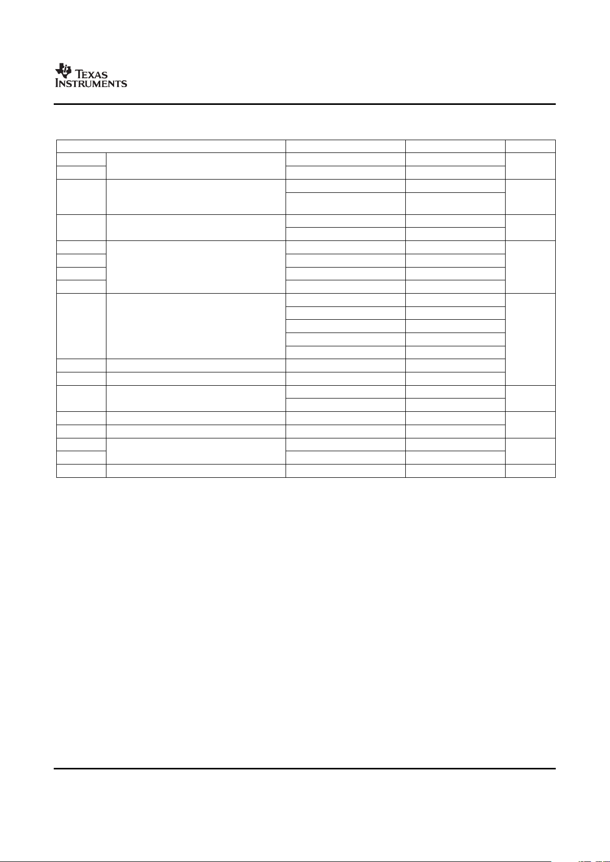
Curre nt
Limit Logic
ILIM
CLF
AGND
3V3
3V3
REG
Driv e andDe ad-Time
Contr olLogic
(D;1-D)
UVLO
I
DLY
+
CS
BIAS
CS+ BST OUT1 SW PVDD OUT2 PGND
Enable
IO
+
0.6 V
POS
NEG
+
AO
VDD
+
ILIM/10
48x
Over
Curre nt
IN
SRE
Blank
UCD7230
DLY
I
LOAD
PWM
SRE
V
OUT
I
DLY
V
IN
BIAS
I
MAX
CLF
UCD7230
SLUS741C – NOVEMBER 2006 – REVISED MARCH 2007
Digital Control Compatible Synchronous Buck Gate Drivers with Current Sense
Conditioning Amplifier
• Digitally-Controlled Synchronous-Buck Power
• Input from Digital Controller Sets Operating
Stages for Single and Multi-Phase
Frequency and Duty Cycle
Applications
• Up to 2-MHz Switching Frequency
• Especially Suited for Use with UCD91xx or
• Dual Current Limit Protection with
UCD95xx Contollers
Independently Adjustable Thresholds
• High-Current Multi-Phase VRM/EVRD
• Fast Current Sense Circuit with Adjustable
Regulators for Desktop, Server, Telecom and
Blanking Interval Prevents Catastrophic
Notebook Processors
Current Levels
• Digitally-Controlled Synchronous-Buck Power
Supplies Using µ Cs or the TMS320TM DSP
• Digital Output Current Limit Flag
Family
• Low Offset, Gain of 48, Differential Current
Sense Amplifier
• 3.3-V, 10-mA Internal Regulator
The UCD7230 is part of the UCD7K family of digital
• Dual TrueDrive™ High-Current Drivers
control compatible drivers for applications utilizing
• 10-ns Typical Rise/Fall Times with 2.2-nF
digital control techniques or applications requiring
Loads
fast local peak current limit protection.
• 4.5-V to 15.5-V Supply Voltage Range
Please be aware that an important notice concerning availability, standard warranty, and use in critical applications of Texas
Instruments semiconductor products and disclaimers thereto appears at the end of this data sheet.
TrueDrive, PowerPAD are trademarks of Texas Instruments.
PRODUCTION DATA information is current as of publication date.
Copyright © 2006–2007, Texas Instruments Incorporated
Products conform to specifications per the terms of the Texas
Instruments standard warranty. Production processing does not
necessarily include testing of all parameters.
Page 2
www.ti.com
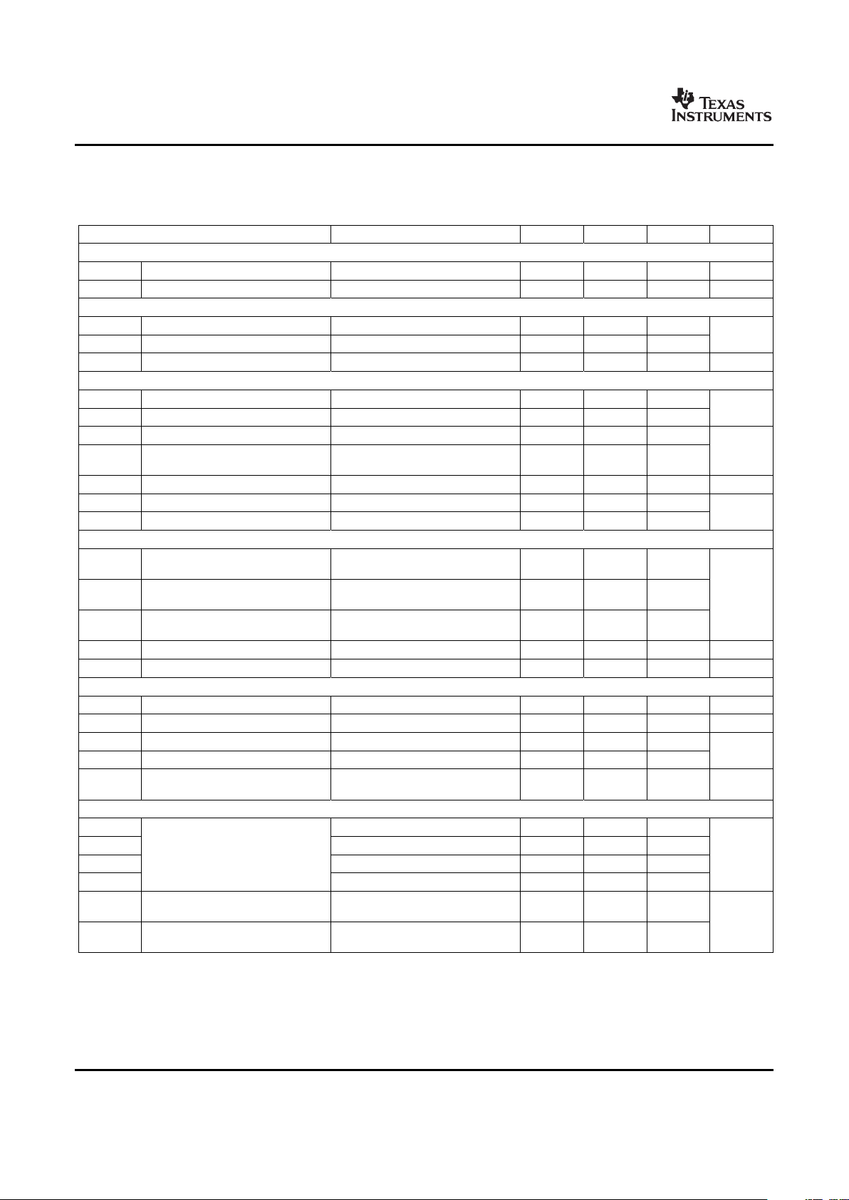
SIMPLIFIED APPLICATION DIAGRAMS
DLY
SRE
AGND
3V3
UCD7230
IN
VDD
DPWMB0
UCD9112
A0
I0
CLF
ILIM
DPWMA0
RB1/TMRI1
OUT1
CSBIAS
SW
6
5
4
2
COMMUNICATION
(Programming&
StatusReporting)
1
VIN
10
7
9
8
OUT2
2
1
3
2
2
ADC2
RB0
AD33
EAP
EAM
VOUT
VOUT
VD25
RST
ADC3
AVSS
2
1
RNEG
RPOS
GSENSE
GSENSE
20
18
CS+
15PVDD
19
17
BST
16
12NEG
14
PGND
13
11POS
UCD7230
SLUS741C – NOVEMBER 2006 – REVISED MARCH 2007
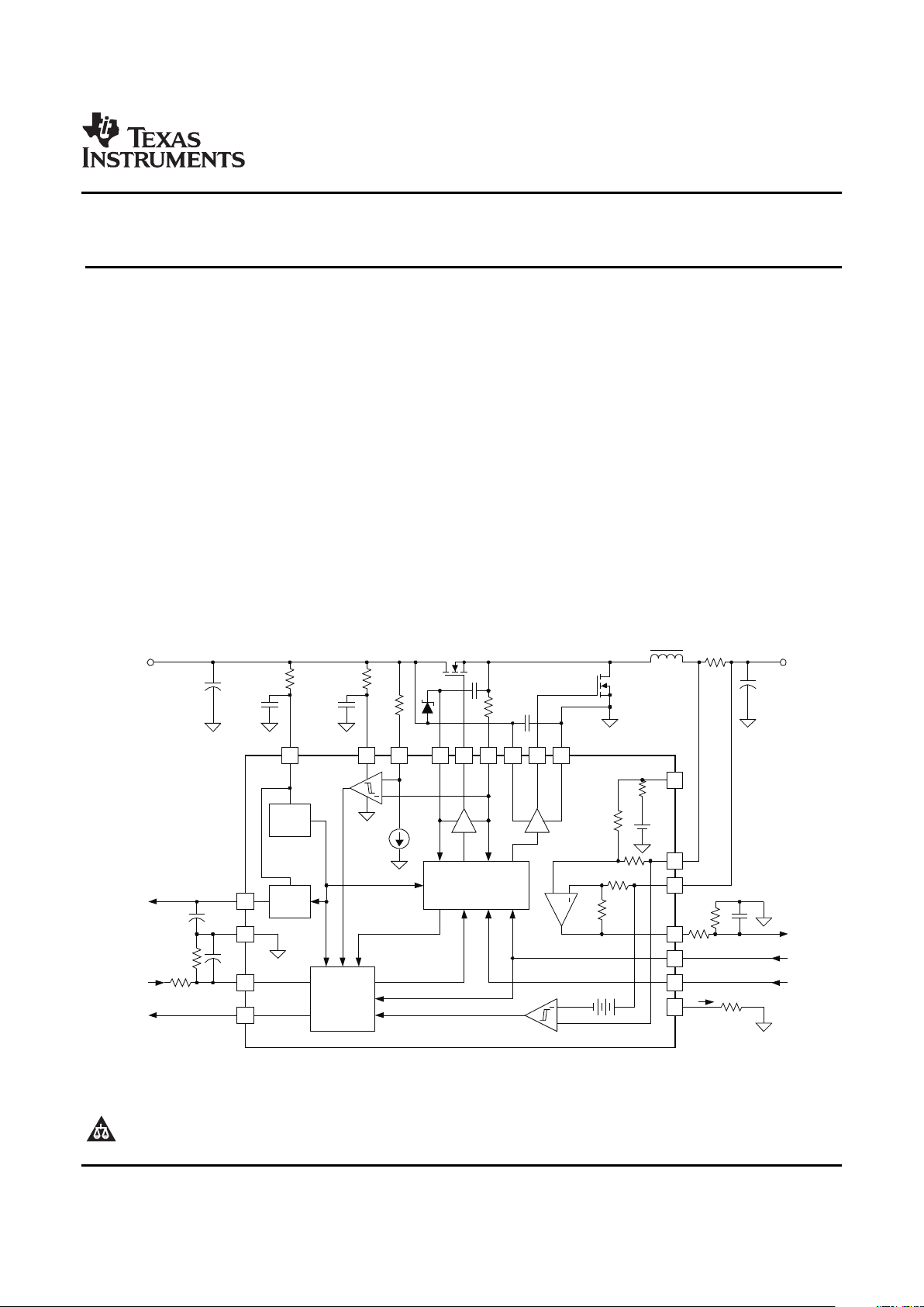
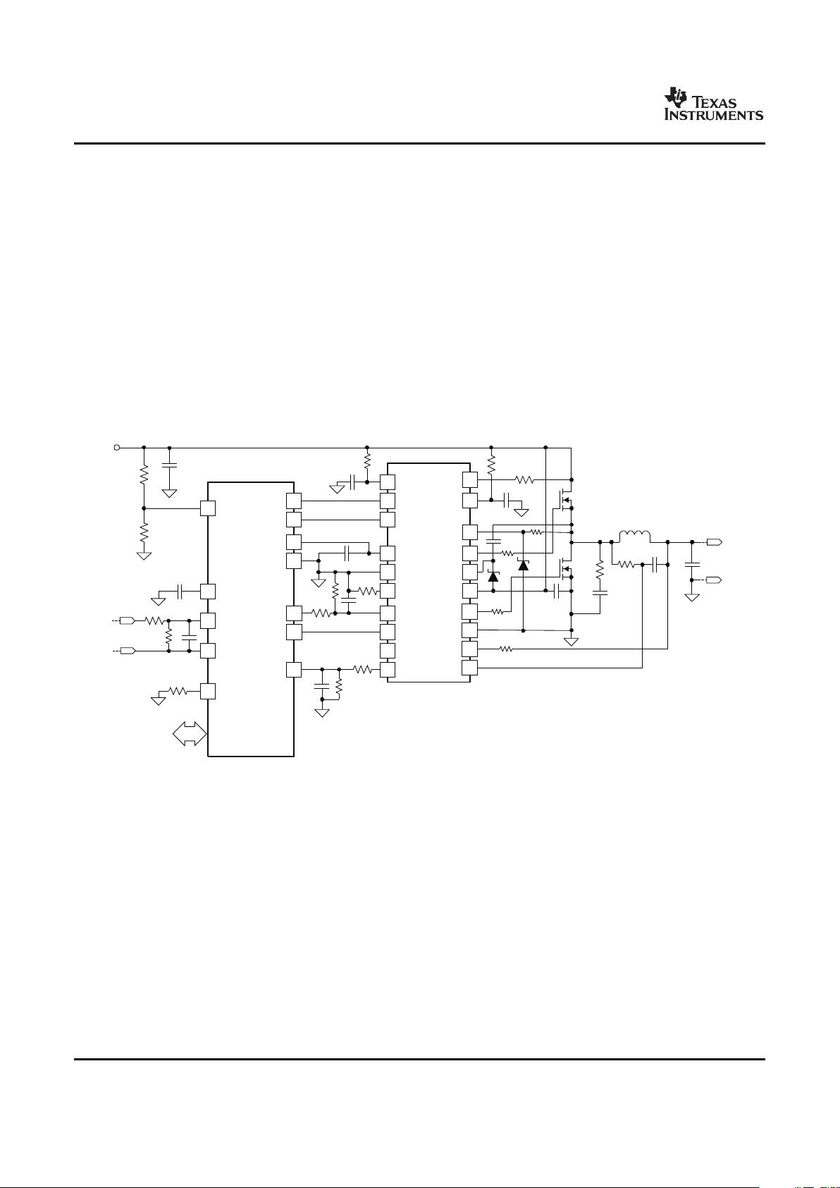
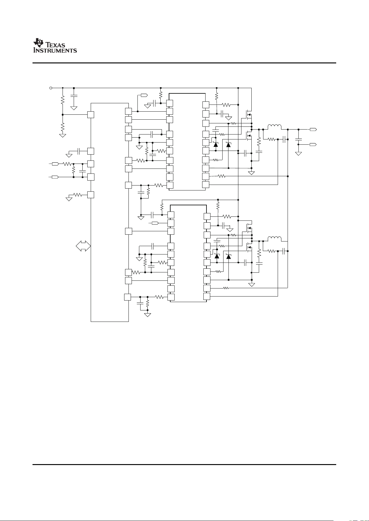
The UCD7230 is a MOSFET gate driver specifically designed for synchronous buck applications. It is ideally
suited to provide the bridge between digital controllers such as the UCD91xx or the UCD95xx and the power
stage. With cycle-by-cycle current limit protection, the UCD7230 device protects the power stage from faulty
input signals or excessive load currents.
The UCD7230 includes high-side and low-side gate drivers which utilize Texas Instrument’s TrueDrive™ output
architecture. This architecture delivers rated current into the gate capacitance of a MOSFET during the Miller
plateau region of the switching. Furthermore, the UCD7230 offers a low offset differential amplifier with a fixed
gain of 48. This amplifier greatly simplifies the task of conditioning small current sense signals inherent in high
efficiency buck converters.
The UCD7230 includes a 3.3-V, 10-mA linear regulator to provide power to digital controllers such as the
UCD91xx. The UCD7230 is compatible with standard 3.3-V I/O ports of the UCD91xx, the TMS320TM family
DSPs, µ Cs, or ASICs.
The UCD7230 is offered in PowerPAD™ HTSSOP or space-saving QFN packages. Package pin out has been
carefully designed for optimal board layout
Figure 1. Single-Phase Synchronous Buck Converter using UCD9112 and one UCD7230
2
Page 3
www.ti.com
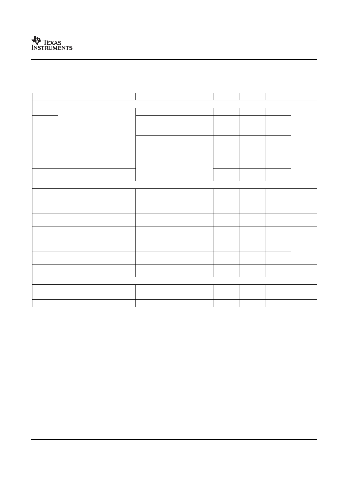
20
18
CS+
OUT1
CSBIAS
SW
15PVDD
2
6
3
5
4
DLY
SRE
AGND
3V3
UCD7230PWP
COMMUNICATION
(Programming&
StatusReporting )
19
17
1
IN
BST
16
1
VDD
VIN
DPWMB0
UCD9112
10
7
9
8
A0
I0
CLF
ILIM
OUT2
12NEG
14
PGND
13
11POS
2
DPWMA0
2
2
ADC2
RB0
AD33
RB1/TMRI1
EAP
EAM
VOUT
VOUT
VD25
RST
ADC3
AVSS
20
18
CS+
OUT1
CSBIAS
SW
15PVDD
2
6
3
5
4
DLY
SRE
AGND
3V3
UCD7230PWP
19
17
1
IN
BST
16
1
VDD
10
7
9
8
A0
I0
CLF
ILIM OUT2
12NEG
14
PGND
13
11POS
2
2
2
2
ADC5
RB3/TMRI0
RB0
RB0
DPWMA1
1
DPWMB1
RPOS1
RNEG1
RPOS2
RNEG2
GSENSE
GSENSE
UCD7230
SLUS741C – NOVEMBER 2006 – REVISED MARCH 2007
SIMPLIFIED APPLICATION DIAGRAMS (continued)
Figure 2. Multi-Phase Synchronous Buck Converter using UCD9112 and two UCD7230
3
Page 4
www.ti.com
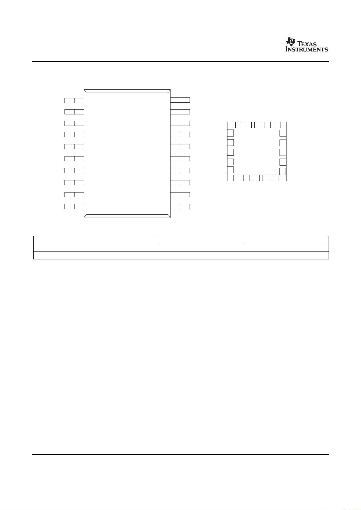
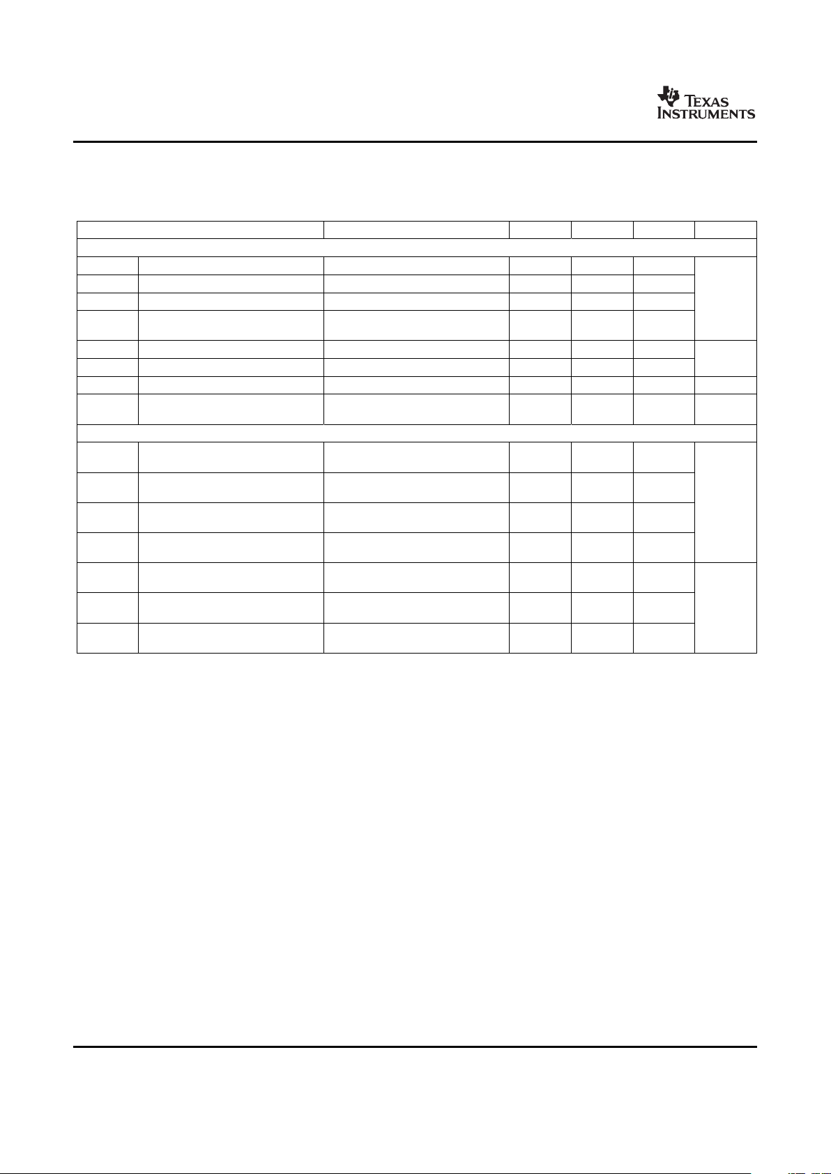
CONNECTION DIAGRAMS
UCD7230
(HTSSOP)
UCD7230
(QFN -
RGW)
(5x5, 0.65)
17
16
15
14
13
12
4
5
6
7
8
9
3V3
AGND
DLY
I0
A0
OUT1
PVDD
OUT2
1110
POS
PGND
ILIM
NEG
CLF
BST
183
IN
SW
4
2
3
10
15
14
13
12
3V3
AGND
DLY
ILIM
SRE
OUT1
BST
PVDD
19 18 17 16
1
7 8 9
CS+
CSBIAS
SW
PGND
NEG
A0
POS
VDD
11 OUT2
6
I0
5
CLF
IN
20
2
1
19
20
SRE
VDD
CSBIAS
CS+
UCD7230
SLUS741C – NOVEMBER 2006 – REVISED MARCH 2007
ORDERING INFORMATION
(1) (2)
PACKAGED DEVICES
TEMPERATURE RANGE
PowerPAD™ HTSSOP-20 (PWP) QFN-20 (RGW)
-40°C to + 125°C UCD7230PWP UCD7230RGW
(1) These products are packaged in Pb-Free and green lead finish of Pd-Ni-Au which is compatible with MSL level 1 at 255-260°C peak
reflow temperature to be compatible with either lead free or Sn/Pb soldering operations.
(2) HTSSOP-20 (PWP), and QFN-20 (RGW) packages are available taped and reeled. Add R suffix to device type (e.g. UCD7230PWPR) to
order quantities of 2,000 devices per reel for the PWP package and 1,000 devices per reel for the RGW packages.
4
Page 5
www.ti.com
ABSOLUTE MAXIMUM RATINGS
(1)
UCD7230
SLUS741C – NOVEMBER 2006 – REVISED MARCH 2007
over operating free-air temperature range (unless otherwise noted)
PARAMETER CONDITION VALUE UNIT
V
DD
16
Supply voltage V
B
ST
SW + 16
I
DD
Quiescent 20
Supply current mA
Switching, TA= 25 ° C, V
DD
= 12
200
V
V
O
OUT1, BST -1 V to 36
Output gate drive voltage V V
OUT2 -1 V to VDD+0.3
I
OUT(sink)
OUT1 4.0
I
OUT(source)
OUT1 -2.0
Output gate drive current A
I
OUT(sink)
OUT2 4.0
I
OUT(source)
OUT2 -4.0
SW -1 to 20
CS+ -0.3 to 20
Analog inputs CSBIAS -0.3 to 16
POS, NEG -0.3 to 5.6 V
ILIM, DLY, I0 -0.3 to 3.6
Analog output A0 -0.3 to 3.6
Digital I/O’s IN, SRE, CLF -0.3 to 3.6
TA= 25 ° C (PWP-20 package) 2.67
Power dissipation W
TA= 25 ° C (QFN-20 package)
T
J
Junction operating temperature -55 to 150
° C
T
stg
Storage temperature -65 to 150
HBM Human body model 2000
ESD rating V
CDM Charged device model 500
Lead temperature (soldering, 10 sec) 300 ° C
(1) Stresses beyond those listed under “absolute maximum ratings” may cause permanent damage to the device. These are stress ratings
only and functional operation of the device at these or any other condition beyond those indicated is not implied. Exposure to absolute
maximum rated conditions for extended periods may affect device reliability. All voltages are with respect to GND. Currents are positive
into, negative out of the specified terminal. Consult company packaging information for thermal limitations and considerations of
packages.
5
Page 6
www.ti.com
ELECTRICAL CHARACTERISTICS
UCD7230
SLUS741C – NOVEMBER 2006 – REVISED MARCH 2007
V
DD
= P
VDD
= 12 V, 4.7- µ F from V
DD
to A
GND
, 1 µ F from P
VDD
to P
GND
, 0.1 µ F from CSBIAS to AGND, 0.22 µ F from BST to
SW, TA= TJ= -40°C to +125°C, R
CS+
= 5 k Ω , R
DLY
= 50 k Ω over operating free-air temperature range (unless otherwise
noted).
PARAMETER TEST CONDITIONS MIN TYP MAX UNIT
SUPPLY
Supply current, off V
DD
= 4.2 V 500 700 µ A
Supply current Outputs not switching IN = LOW 5 8 mA
LOW-VOLTAGE UNDER-VOLTAGE LOCKOUT
VDD UVLO ON V
DD
rising 4.25 4.50 4.75
V
VDD UVLO OFF V
DD
falling 4.00 4.25 4.50
VDD UVLO hysteresis 100 250 400 mV
REFERENCE / EXTERNAL BIAS SUPPLY
3V3 initial set point TA= 25 ° C 3.267 3.3 3.333
V
3V3 over temperature 3.234 3.3 3.366
3V3 load regulation I
LOAD
= 1 mA to 10 mA, V
DD
= 5V 1 7
mV
V
DD
= 4.75 V to 12 V, I
LOAD
= 10
3V3 line regulation 3 10
mA
Short circuit current V
DD
= 4.75 V to 12 V 11 20 mA
3V3 OK threshold, ON 3.3 V rising 2.8 3 3.2
V
3V3 OK threshold, OFF 3.3 V falling 2.6 2.8 3.0
INPUT SIGNAL (IN)
Positive-going input threshold
INHigh 1.6 1.9 2.2
voltage
Negative-going input threshold
INLow 1.0 1.3 1.6 V
voltage
INHigh –
Input voltage hysteresis 0.4 0.6 0.8
INLow
Input resistance to AGND 50 100 150 k Ω
Frequency ceiling 2 MHz
CURRENT LIMIT (ILIM)
ILIM internal voltage setpoint I
LIM
=OPEN 0.47 0.50 0.53 V
ILIM input impedance 20 42 65 k Ω
CLF output high level I
LOAD
= 4 mA 2.7
V
CLF output low level I
LOAD
= 4 mA 0.6
Propagation delay from IN to reset 2nd IN rising to CLF falling after a
15 35 ns
CLF current limit event
CURRENT SENSE COMPARATOR (OUTPUT SENSE)
I
LIM
= open 40 50 60
I
LIM
= 3.3 V 80 100 120
CS threshold (POS - NEG) mV
I
LIM
= 0.75 V 60 75 90
I
LIM
= 0.25 V 15 25 35
Propagation delay from POS to
I
LIM
= open, CS = threshold + 60 mV 90
OUT1 falling
(1)
ns
Propagation delay from POS to
I
LIM
= open, CS = threshold + 60 mV 100
CLF
(1)
(1) As designed and characterized. Not 100% tested in production.
6
Page 7
www.ti.com
UCD7230
SLUS741C – NOVEMBER 2006 – REVISED MARCH 2007
ELECTRICAL CHARACTERISTICS (continued)
V
DD
= P
VDD
= 12 V, 4.7- µ F from V
DD
to A
GND
, 1 µ F from P
VDD
to P
GND
, 0.1 µ F from CSBIAS to AGND, 0.22 µ F from BST to
SW, TA= TJ= -40°C to +125°C, R
CS+
= 5 k Ω , R
DLY
= 50 k Ω over operating free-air temperature range (unless otherwise
noted).
PARAMETER TEST CONDITIONS MIN TYP MAX UNIT
CURRENT SENSE COMPARATOR (INPUT SENSE)
R
DLY
= 24.3 k Ω (CSBIAS-CS+) 170 235 300
CS threshold mV
R
DLY
= 49.9 k Ω (CSBIAS-CS+) 90 114 140
R
DLY
= 24.3 k Ω , IN rising to OUT1,
120
IN falling to OUT2, VDD = 6 V
CS blanking time
(2)
ns
R
DLY
= 49.9 k Ω , IN rising to OUT1,
230
IN falling to OUT2, VDD = 6 V
R
DELAY
range
(2)
24.3 50.0 100.0 k Ω
Propagation delay from CS+ to
80
OUT1
(2)
CS = threshold + 60mV ns
Propagation delay from CS+ to
70
CLF
(2)
CURRENT SENSE AMP
I0 = OPEN; POS = NEG = 1.25 V;
V
OO
Output offset voltage -100 0 100 mV
measure AO - IO
I0 = FLOAT; V
POS
= 1.26 V; V
NEG
=
Closed loop dc gain 46 48 50 V/V
1.25 V, R
POS
= R
NEG
= 0
POS = 1.25 V, NEG = 1.29 V,R =
Input impedance 5.5 8.3 12 k Ω
(POS - NEG) / (I
POS
- I
NEG
)
V
CM(max)
is limited to (V
DD
-1.2V),
V
CM
Input Common Mode Voltage Range 0 5.6 V
R
POS
= 0
V
POS
= 1.2 V; V
NEG
= 1.3 V;
A0_Vol Minimum Output Voltage 0.15 0.3
A0_I
SINK
= 250 µ A
V
V
POS
=1.3 V; V
NEG
= 1.2 V; A0_
A0_Voh Maximum Output Voltage 3 3.1 3.5
I
SOURCE
= 500 µ A
I0 = FLOAT; V
POS
= V
NEG
= 0.8 V to
Input Bias Current, POS or NEG -2 30 µ A
5.0 V, R
POS
= R
NEG
= 0
ZERO CURRENT REFERENCE (IO)
Reference voltage Measured at I0 0.54 0.6 0.66 V
Input transition voltage With respect to IO reference 10 60 120 mV
I
O
Output impedance I
ZERO
= 0.6 V 10 15 21 k Ω
(2) As designed and characterized. Not 100% tested in production.
7
Page 8
www.ti.com
UCD7230
SLUS741C – NOVEMBER 2006 – REVISED MARCH 2007
ELECTRICAL CHARACTERISTICS (continued)
V
DD
= P
VDD
= 12 V, 4.7- µ F from V
DD
to A
GND
, 1 µ F from P
VDD
to P
GND
, 0.1 µ F from CSBIAS to AGND, 0.22 µ F from BST to
SW, TA= TJ= -40°C to +125°C, R
CS+
= 5 k Ω , R
DLY
= 50 k Ω over operating free-air temperature range (unless otherwise
noted).
PARAMETER TEST CONDITIONS MIN TYP MAX UNIT
LOW-SIDE OUTPUT DRIVER (OUT2)
Source current
(3)
V
DD
= 12 V, IN = high, OUT2 = 5 V 2.2
Sink current
(3)
V
DD
= 12 V, IN = low, OUT2 = 5 V 3.5
A
Source current
(3)
V
DD
= 4.75 V, IN = high, OUT2 = 0 1.6
V
DD
= 4.75 V, IN = low, OUT2 =
Sink current
(3)
2
4.75 V
Rise time
(3)
C
LOAD
= 2.2 nF, V
DD
= 12 V 15
ns
Fall time
(3)
C
LOAD
= 2.2 nF, V
DD
= 12 V 15
Output with VDD <UVLO V
DD
= 1.0 V, Isink = 10 mA 0.8 1.2 V
Propagation delay from IN to C
LOAD
= 2.2 nF, IN rising, SW = 2.5
30 ns
OUT2
(3)
V, BST = PVDD = VDD = 12 V
HIGH-SIDE OUTPUT DRIVER (OUT1)
V
DD
= 12 V, BST = 12 V IN = High,
Source current
(3)
1.7
OUT1 = 5 V
V
DD
= 12 V, BST = 12 V IN = Low,
Sink current
(3)
3.5
OUT1 = 5 V
A
V
DD
= 4.75 V = BST = 4.75 V, IN =
Source current
(3)
1
High, OUT1 = 0
V
DD
= 4.75 V, BST = 4.75 V, IN =
Sink current
(3)
2.4
Low, OUT1 = 4.75 V
C
LOAD
= 2.2 nF OUT1 to SW, VDD
Rise time
(3)
20
= 12 V
C
LOAD
= 2.2 nF OUT1 to SW, V
DD
=
Fall time
(3)
15 ns
12 V
Propagation delay from IN to C
LOAD
= 2.2 nF, IN falling, SW = 2.5
30
OUT1
(3)
V, BST = PVDD = VDD = 12 V
(3) As designed and characterized. Not 100% tested in production.
8
Page 9

www.ti.com
DEVICE INFORMATION
UCD7230
SLUS741C – NOVEMBER 2006 – REVISED MARCH 2007
TERMINAL FUNCTIONS
TERMINAL
UCD7230
I/O DESCRIPTION
NAME
HTSSOP-
QFN-20
20
Supply input pin to power the internal circuitry except the driver outputs. The
VDD 1 18 -
UCD7230 accepts an input range of 4.5 V to 15.5 V.
Synchronous Rectifier Enable. The SRE pin is a high impedance digital input
capable of accepting 3.3-V logic level signals, used to disable the synchronous
SRE 2 19 I
rectifier switch. The synchronous rectifier is disabled when this signal is low. A
Schmitt trigger input comparator desensitizes this pin from external noise.
The IN pin is a high impedance digital input capable of accepting 3.3-V logic
IN 3 20 I level signals up to 2 MHz. A Schmitt trigger input comparator desensitizes this
pin from external noise.
Regulated 3.3-V rail. The onboard linear voltage regulator is capable of
3V3 4 1 O sourcing up to 10 mA of current. Bypass with 0.22- µ F ceramic capacitance
from this pin to analog ground, AGND.
AGND 5 2 - Analog ground return.
Requires a resistor to AGND for setting the current sense blanking time for
both the high-side and low-side current sense comparators. The value of this
DLY 6 3 I
resistor in conjunction with the resistor in series with the CS+ pin sets the high
side current sense threshold.
Output current limit threshold set pin. The output current threshold is 1/10
th
of
the value set on this pin. If left floating the voltage on this pin is 0.55 V. The
ILIM 7 4 I
voltage on the ILIM pin can range from 0.25 V to 1V to set the threshold from
25 mV to 100 mV.
Current Limit Flag. The CLF signal is a 3.3-V digital output which is latched
CLF 8 5 O high after an over current event, triggered by either of the two current sense
comparators and reset after two rising edges received on the IN pin.
Sets the current sense linear amplifier “Zero” output level. The default value is
IO 9 6 I
0.6 V which allows negative current measurement.
Current sense linear amplifier output. The output voltage level on this pin
AO 10 7 O represents the average output current. Any value below the level on the I0 pin
represents negative output current.
Non-inverting input of the output current sense amplifier and current limit
POS 11 8 I
comparator.
Inverting input of the output current sense amplifier and current limit
NEG 12 9 I
comparator.
Power ground return. This pin should be connected close to the source of the
PGND 13 10 -
low-side synchronous rectifier MOSFET.
The low-side high-current TrueDrive™ driver output. Drives the gate of the
OUT2 14 11 I
low-side synchronous MOSFET between PVDD and PGND.
Supply pin provides power for the output drivers. It is not connected internally
PVDD 15 12 - to the VDD supply rail. The bypass capacitor for this pin should be returned to
PGND.
Floating OUT1 driver supply powered by an external Schottky diode from the
BST 16 13 I
PVDD pin during the synchronous MOSFET on time.
The high-side high-current TrueDrive™ driver output. Drives the gate of the
OUT1 17 14 I
high-side buck MOSFET between SW and BST.
SW 18 15 I/O OUT1 gate drive return and square wave input to output inductor.
CSBIAS 19 16 I Supply pin for the high-side current sense comparator.
Non-inverting Input for the high side current sense comparator. A resistor
CS+ 20 17 I connected between this pin and the high side MOSFET drain, in conjunction
with the DLY resistor sets the high-side current limit threshold.
9
Page 10

www.ti.com
APPLICATION INFORMATION
Introduction
Supply Requirements
Reference / External Bias Supply
Control Inputs
UCD7230
SLUS741C – NOVEMBER 2006 – REVISED MARCH 2007
The UCD7230 is a synchronous buck driver with peak-current limiting. It is a member of the UCD7K family of
digital compatible drivers suitable either for applications utilizing digital control techniques or analog applications
that require local fast peak current limit protection.
In systems using the UCD7230, the feedback loop is closed externally and the IN signal represents the PWM
information required to regulate the output voltage. The PWM signal may be implemented by either a digital or
analog controller.
The UCD7230 has two over-current protection features, one that limits the peak current in the high-side switch
and one that limits the output current. Both limits are individually programmable. The internal current sense
blanking enables ease of design with real-world signals. In addition to over current limit protection, current sense
signals can be conditioned by the on board amplifier for use by the system controller.
The UCD7230 operates on a supply range of 4.5 V to 15.5 V. The supply voltage should be applied to three
pins, PVDD, VDD, and CSBIAS. PVDD is the supply pin for the lower driver, and has the greatest current
demands. The supply connection to PVDD is also the point where an external Schottky diode provides current to
the high side flying driver. PVDD should be bypassed to PGND with a low ESR ceramic capacitor. In the same
fashion, the flying driver should be bypassed between BST and SW.
VDD and CSBIAS are less demanding supply pins, and should be resistively coupled to the supply voltage for
isolation from noise generated by high current switching and parasitic board inductance. Use 33 Ω for CSBIAS
and 1 Ω for VDD. VDD should be bypassed to AGND with a 4.7- µ F ceramic capacitor while CSBIAS should be
bypassed to AGND with 0.1 µ F. Although the three supply pins are not internally connected, they must be
biased to the same voltage. It is important that all bypassing be done with low parasitic inductance techniques to
good ground planes.
PGND and AGND are the ground return connections to the chip. Ground plane construction should be used for
both pins. For a MOSFET driver operating at high frequency, it is critical to minimize the stray inductance to
minimize overshoot, undershoot, and ringing. The low output impedance of the drivers produces waveforms with
high di/dt. This induces ringing in the parasitic inductances. It is highly desirable that the UCD7230 and the
MOSFETs be collocated. PGND and the AGND pins should be connected to the PowerPAD™ of the package
with two thin traces. It is critical to ensure that the voltage potential between these two pins does not exceed 0.3
V.
Although quiescent VDD current is low, total supply current depends on the gate drive output current required for
the capacitive load and the switching frequency. Total supply current is the sum of quiescent VDD current and
the average OUT current. Knowing the operating frequency and the MOSFET gate charge (Qg), average OUT
current can be calculated from (I
OUT
= Qg x f), where f is the operating frequency.
The UCD7230 includes a series pass regulator to provide a regulated 3.3 V at the 3V3 pin that can be used to
power other circuits such as the UCD91xx, a microcontroller or an ASIC. 3V3 can source 10 mA of current. For
normal operation, place a 0.22- µ F ceramic capacitor between 3V3 and AGND.
IN and SRE are high impedance digital inputs designed for 3.3-V logic-level signals. They both have 100-k Ω
pull-down resistors. Schmitt Trigger input stage design immunizes the internal circuitry from external noise. IN is
the command input for the upper driver, OUT1, and can function up to 2 MHz. SRE controls the function of the
lower driver, OUT2. When SRE is false (low), OUT2 is held low. When SRE is true, OUT2 is inverted from OUT1
with appropriate delays that preclude cross conduction in the Buck MOSFETs.
10
Page 11

www.ti.com
Driver Stages
0 1 2 4 5 6
OUT2 - V
0
1.0
2.0
3.0
4.0
5.0
3
0.5
1.5
2.5
3.5
4.5
I
SOURCE
/I
SINK
- Source Current/Sink Current - A
Sink Current
VDD = 12 V
Sink Current
VDD = 5 V
Source Current
VDD = 12 V
Source Current
VDD = 5 V
OUT2 SOURCE/SINK CURRENT
vs
OUT2 VOLTAGE
0 1 2 4 5 6
OUT1 - SW - V
0
1.0
2.0
3.0
4.0
5.0
3
0.5
1.5
2.5
3.5
4.5
I
SOURCE
/I
SINK
- Source Current/Sink Current - A
Sink Current
VDD = 12 V
Sink Current
VDD = 5 V
Source Current
VDD = 12 V
Source Current
VDD = 5 V
OUT1 SOURCE/SINK CURRENT
vs
OUT1 VOLTAGE WITH RESPECT TO SW VOLTAGE
UCD7230
SLUS741C – NOVEMBER 2006 – REVISED MARCH 2007
APPLICATION INFORMATION (continued)
The driver outputs utilize Texas Instruments’ TrueDrive™ architecture, which delivers rated current into the gate
of a MOSFET when it is most needed, during the Miller plateau region of the switching transition. This provides
best switching speeds and reduces switching losses. TrueDrive™ consists of pull-up/ pull-down circuits using
bipolar and MOSFET transistors in parallel. This hybrid output stage also allows relatively constant current
sourcing even at reduced supply voltages.
The low-side high-current output stage of the UCD7230 device is capable of sourcing 1.7-A and sinking 3.5-A
current pulses and swings from PVDD to PGND. The high-side floating output driver is capable of sourcing 2.2-A
and sinking 3.5-A peak-current pulses. This ratio of gate currents, common to synchronous buck applications,
minimizes the possibility of parasitic turn on of the low-side power MOSFET due to dv/dt currents during the
rising edge switching transition. See the typical curves of sink and source current in Figure 3 and Figure 4
below.
If further limiting of the rise or fall times to the power device is desired, an external resistance can be added
between the output of the driver and the power MOSFET gate. The external resistor also helps remove power
dissipation from the driver.
Driver outputs follow IN and SRE as previously described provided that VDD and 3V3 are above their respective
under-voltage lockout thresholds. When the supplies are insufficient, the chip holds both OUT1 and OUT2 low.
It is worth reiterating the need mentioned in the supply section for sound high frequency design techniques in
the circuit board layout and bypass capacitor selection and placement. Some applications may generate
excessive ringing at the switch-inductor node. This ringing can drag SW to negative voltages that might cause
functional irregularities. To prevent this, carefull board layout and appropriate snubbing are essential. In addition,
it may be appropriate to couple SW to the inductor with a 1- Ω resistor, and then bypass SW to PGND with a low
impedance Schottky diode.
Figure 3. Figure 4.
11
Page 12

www.ti.com
Current Sensing and Overload Protection
48
OUT SHUNT
AO ( I R ) IO= ´ ´ +
POS
NEG AO
I0
+
+
V
OUT
SW
L
8.33 kΩ 400kΩ
8.33 kΩ 400 kΩ
Curre ntSen seAmp
IO Buffe r
Amp
R
SHUNT
POS
NEG AO
I0
+
+
SW
C
L
+
R
8.33 kΩ
R
NEG
R
POS
400 kΩ
8.33 kΩ 400k Ω
Curre ntSen seAmp
IO Buffe r
Amp
V
OUT
C
OUT
C
OUT
OUT COPPER
AO ( A I R ) IO= ´ ´ +
UCD7230
SLUS741C – NOVEMBER 2006 – REVISED MARCH 2007
APPLICATION INFORMATION (continued)
Since the UCD7230 is physically collocated with the high-current elements of the power converter, it is logical
that current be monitored by the chip. An internal instrumentation amplifier conditions current sense signals so
that they can be used by the control chip generating the PWM signal.
POS and NEG are inputs to an instrumentation amplifier circuit. This amplifier has a nominal gain of 48 and
presents its output at AO. This can be used to monitor either an external current sense shunt or a parallel RC
around the buck inductor shown in Figure 5 . The shunt yields the highest accuracy and will be insensitive to
inductor core saturation effects. It comes with the price of added power dissipation. Using the shunt, AO is given
by:
The internal configuration of the instrumentation amplifier is such that AO is 0.6 V when POS – NEG = 0.
Because of this output offset, the amplifier can accurately pass information for both positive and negative load
current. The offset is controlled by IO. If IO is left to float, the offset is 0.6 V. 0.6 V is present at IO through an
internal 10-k Ω resistor and should be bypassed to AGND. If a higher value of offset is desired, a voltage in
excess of 0.66 V can be externally applied to IO. Once IO is forced above 0.66 V, the internal 10 k Ω is
disconnected, and the AO output offset is now equal to the voltage applied to IO.
Figure 5. Current Sense Using External Shunt and Lossless Average Output Current Sensing Using DC
Resistance of the Output Inductor.
Figure 5 also shows lossless current sensing utilizing an RC across the buck inductor to generate an analog of
the IR drop on the copper of the inductor. As long as the R
POS
x C time constant is the same as the L/R of the
inductor and its parasitic equivalent series resistance, then the voltage on C is the same as the IR drop on the
parasitic inductor resistance. A resistor, R
NEG
= R
POS
is used for amplifier bias current cancellation. The transfer
function of the amplifier is given by:
12
Page 13

www.ti.com
48
1
8 33
POS
A
R
. k
=
æ ö
+
ç ÷
W
è ø
0 500 1500 2000
R
POS
- W
49
1000
Amp Gain - V/V
Current Sense AMP Gain
vs
RPOS
Normal Gain
Minimum Gain Corner
(minimum sheet and hot
temperature)
Maximum Gain Corner
(minimum sheet and Cold
temperature)
48
47
46
45
44
43
42
41
40
39
38
37
36
35
UCD7230
SLUS741C – NOVEMBER 2006 – REVISED MARCH 2007
APPLICATION INFORMATION (continued)
With the addition of R
POS
and R
NEG
, the natural gain, A, of the current sense is predictably decreased as:
For R
POS
<< 8.33 k Ω , the gain is 48. While the 400 k Ω and 8.33 k Ω are well matched, it is important to keep
R
POS
as small as possible since they have absolute variation from chip-to-chip and over temperature. The graph
in Figure 6 shows the band of expected gain for A as a function of R
POS
. The gain variation at R
POS
= 1 k Ω
results in around ±4% error. However, the tolerance of the value of R in the inductor has a more significant
effect on measurement accuracy as does the temperature coefficient of R. Copper has a temperature coefficient
of approximately 3800 ppm/°C. For a 100°C rise in winding temperature, the dc resistance of the inductor
increases by 38%. The worst case scenario would be a cracked core or under-designed inductor in which cases
the core could tend towards saturation. In that scenario, inductor current could change slope drastically and is
not correctly modeled by the capacitor voltage.
Note that inferring inductor current by use of a parallel RC has an additional caveat. As long as T
RC
= R
POS
C is
the same as T
LR
= L/R, then the voltage across C is the same as the IR drop across the equivalent R of the
inductor. If the time constants don't match, the average voltage across C is still the same as the average voltage
across R, but the indication of ripple current amplitude will be off. Furthermore, load transients results in reported
current that appears to have overshoot or undershoot if T
RC
is respectively faster or slower than T
LR
.
While the amp faithfully passes the sensed dc current signal, it should be noted that the amplifier is bandwidth
limited for normal switching frequencies. Therefore, AO represents a moving average of the sensed current.
Figure 6. Current Sense Amp Gain as a Function of R
POS
13
Page 14

www.ti.com
To
A/D
A0
5
BLANK DLY
t ( ns ) R ( k )» W
1 2
CS
CS( in )
DLY
R
V .
R
+
æ ö
= ´
ç ÷
è ø
10
LIM
CS( out )
I
V =
UCD7230
SLUS741C – NOVEMBER 2006 – REVISED MARCH 2007
APPLICATION INFORMATION (continued)
The amp output can go up to 3.3 V, so reasonable designs limits full scale to 3.0 V. Should attenuation be
necessary, use a resistive divider between AO and the control chip A/D input as shown in Figure 7 .
Figure 7. Attenuating and Filtering the Voltage Representation of the Average Output Current
While the current sense amplifier is useful for accurate current monitoring or controlling overload conditions,
extreme overload conditions must be handled in timeframes that are generally much shorter than the A/D of a
control chip can achieve. Therefore, there are two comparators on the UCD7230 to sense extreme overload and
protect the driven power MOSFETs.
Extreme current overload is handled in two ways by the UCD7230. One is a comparator that monitors the
voltage between POS and NEG, or effectively the output current of the converter.. The other is a comparator
that monitors the voltage drop across the high-side MOSFET, or effectively the input current. Should either
condition exceed a preset value, OUT1 is immediately turned off for the remainder of the cycle.
To program the current limit, a value of resistance from DLY to AGND must first be chosen to establish a
blanking time during which the comparators will be blinded to switching noise. The blanking time starts with the
rising edge on IN for the input comparator and from both the rising and falling edge of IN for the output
comparator. Blanking time is given by:
where R
DLY
is the resistor from DLY to AGND. R
DLY
should be limited to a range of 25 k Ω to 100 k Ω .
Once R
DLY
has been chosen, the threshold for the input comparator, i.e., the drop allowed across the high-side
MOSFET, is given by:
Where V
CS(in)
is the threshold of allowed voltage across the high-side MOSFET and RCS+ is a resistor
connected from CS+ to the drain of the high-side MOSFET.
The blanking time for the output comparator is identical to the input comparator. The output comparator
threshold is given by:
where V
CS(out)
is the threshold of allowed voltage between the POS and NEG pins and I
LIM
is the voltage on the
ILIM pin. Note that the ILIM is internally connected to 0.5 V through a 42 k Ω resistor. Any voltage between 0.25
V and 1.0 V can be applied to ILIM. For voltages above 1.0 V, the maximum V
CS(OUT)
threshold is clamped to 0.1
V. Possible methods for setting ILIM are shown in Figure 8 .
When using the output comparator to monitor the voltage on the parallel sensing capacitor across the inductor,
the same caveats apply as described for the current sense amplifier.
14
Page 15

www.ti.com
UCD7230
DIGITAL
CONTROLLER
AGND
3V3
ILIM
GPIO1
VCC
GND
GPIO2
GPIO3
GPIO4
2.5 kW
40 kW
ILIM SETPOINT
[Volts] GPIO3 GPIO2 GPIO1 GPIO4
ILIM (open) 0.50 OPEN OPEN OPEN OPEN
ILIM0 0.00 0 0 0 0
ILIM1 0.14 0 0 1 0
ILIM2 0.29 0 1 0 0
ILIM3 0.43 0 1 1 0
ILIM4 0.57 1 0 0 0
ILIM5 0.72 1 0 1 0
ILIM6 0.86 1 1 0 0
ILIM7 1.00 1 1 1 0
DIGITAL
CONTROLLER
PWM
Rf
Rf and Cf filter the PWM
output to generate a DC
input to the ILIM PIN
A) GPIO Outputs
B) PWM Output
UCD7230
AGND
3V3
ILIM
Cf
C) Resistor Divider
D) Internal Set Point
20 kW
10 kW
UCD7230
AGND
3V3
ILIM
GND
VCC
DIGITAL
CONTROLLER
R1
UCD7230
AGND
3V3
ILIM
GND
VCC
R2
Cf
UCD7230
SLUS741C – NOVEMBER 2006 – REVISED MARCH 2007
APPLICATION INFORMATION (continued)
Figure 8. Setting the ILIM Voltage with: a) GPIO Outputs, b) PWM Output, c) Resistor Divider, d) Internal
Set Point
15
Page 16

www.ti.com
Startup Handshaking
Thermal Management
REFERENCES
RELATED PRODUCTS
UCD7230
SLUS741C – NOVEMBER 2006 – REVISED MARCH 2007
APPLICATION INFORMATION (continued)
If either comparator threshold is exceeded, OUT1 is immediately turned off for the remainder of the cycle and
CLF is asserted true. Upon the rising edge of IN, the switches resume normal operation, but the CLF assertion
is maintained. If a fault is not detected in this switching cycle, then the next rising edge of IN removes the CLF
assertion. However, if one of the comparators detects a fault, then CLF assertion continues. It is the privilege of
the control device to monitor CLF and decide how to handle the fault condition. In the mean while, the protection
comparators protect the power MOSFET switches on a cycle-by-cycle basis. If the output-sense comparator
(POS - NEG) detects continuous over-current, then the driver assumes 0% duty cycle until the current drops to a
safe value. Note that when a fault condition causes OUT1 to be driven low, OUT2 behaves as if the input pulse
had been terminated normally. In some fault conditions, it is advantageous to drive OUT2 low. SRE can be used
to cause OUT2 to remain low at the discretion of the control chip. This can be used to achieve faster discharge
of the inductor and also to fully disconnect the converter from the output voltage.
The UCD7230 has a built-in handshaking feature to facilitate efficient start-up of the digitally controlled power
supply. At start-up the CLF flag is held high until all the internal and external supply voltages of the device are
within their operating range. Once the supply voltages are within acceptable limits, CLF goes low and the device
will process input commands. The digital controller should monitor CLF at start-up and wait for CLF to go low
before sending pwm information to the UCD7230.
The usefulness of a driver is greatly affected by the drive power requirements of the load and the thermal
characteristics of the device package. In order for a power driver to be used over a particular temperature range,
the package must allow for the efficient removal of the heat while keeping the junction temperature within rated
limits. The UCD7230 is available in PowerPAD™ HTSSOP and QFN packages to cover a range of application
requirements. Both have the exposed pads to remove thermal energy from the semiconductor junction.
As illustrated in Reference [3 & 4], the PowerPAD™ packages offer a lead-frame die pad that is exposed at the
base of the package. This pad is soldered to the copper on the PC board (PCB) directly underneath the device
package, reducing the θ
JA
down to 38 ° C/W. The PC board must be designed with thermal lands and thermal
vias to complete the heat removal subsystem, as summarized in Reference [3].
Note that the PowerPAD™ is not directly connected to any leads of the package. However, it is electrically and
thermally connected to the substrate which is the ground of the device. The PowerPAD™ should be connected
to the quiet ground of the circuit.
1. Power Supply Seminar SEM-1600 Topic 6: A Practical Introduction to Digital Power Supply Control, by
Laszlo Balogh, Texas Instruments Literature No. SLUP224
2. Power Supply Seminar SEM–1400 Topic 2: Design and Application Guide for High Speed MOSFET Gate
Drive Circuits, by Laszlo Balogh, Texas Instruments Literature No. SLUP133.
3. Technical Brief, PowerPad Thermally Enhanced Package, Texas Instruments Literature No. SLMA002
4. Application Brief, PowerPAD™ Made Easy, Texas Instruments Literature No. SLMA004
RELATED PRODUCTS
PRODUCT DESCRIPTION FEATURES
UCD9501 Digital power controller for high performance multi-loop applications
UCD9111 Digital power controller for power supply applications
UCD9112 Digital power controller for power supply applications
16
Page 17

TAPE AND REEL INFORMATION
*All dimensions are nominal
Device Package
Type
Package
Drawing
Pins SPQ Reel
Diameter
(mm)
Reel
Width
W1 (mm)
A0 (mm) B0 (mm) K0 (mm) P1
(mm)W(mm)
Pin1
Quadrant
UCD7230PWPR HTSSOP PWP 20 2000 330.0 16.4 6.95 7.1 1.6 8.0 16.0 Q1
UCD7230RGWR QFN RGW 20 3000 330.0 12.4 5.3 5.3 1.5 8.0 12.0 Q2
UCD7230RGWT QFN RGW 20 250 180.0 12.4 5.3 5.3 1.5 8.0 12.0 Q2
PACKAGE MATERIALS INFORMATION
www.ti.com
11-Mar-2008
Pack Materials-Page 1
Page 18

*All dimensions are nominal
Device Package Type Package Drawing Pins SPQ Length (mm) Width (mm) Height (mm)
UCD7230PWPR HTSSOP PWP 20 2000 346.0 346.0 33.0
UCD7230RGWR QFN RGW 20 3000 346.0 346.0 29.0
UCD7230RGWT QFN RGW 20 250 190.5 212.7 31.8
PACKAGE MATERIALS INFORMATION
www.ti.com
11-Mar-2008
Pack Materials-Page 2
Page 19

Page 20

Page 21

Page 22

Page 23

Page 24

Page 25

IMPORTANT NOTICE
Texas Instruments Incorporated and its subsidiaries (TI) reserve the right to make corrections, modifications, enhancements, improvements,
and other changes to its products and services at any time and to discontinue any product or service without notice. Customers should
obtain the latest relevant information before placing orders and should verify that such information is current and complete. All products are
sold subject to TI’s terms and conditions of sale supplied at the time of order acknowledgment.
TI warrants performance of its hardware products to the specifications applicable at the time of sale in accordance with TI’s standard
warranty. Testing and other quality control techniques are used to the extent TI deems necessary to support this warranty. Except where
mandated by government requirements, testing of all parameters of each product is not necessarily performed.
TI assumes no liability for applications assistance or customer product design. Customers are responsible for their products and
applications using TI components. To minimize the risks associated with customer products and applications, customers should provide
adequate design and operating safeguards.
TI does not warrant or represent that any license, either express or implied, is granted under any TI patent right, copyright, mask work right,
or other TI intellectual property right relating to any combination, machine, or process in which TI products or services are used. Information
published by TI regarding third-party products or services does not constitute a license from TI to use such products or services or a
warranty or endorsement thereof. Use of such information may require a license from a third party under the patents or other intellectual
property of the third party, or a license from TI under the patents or other intellectual property of TI.
Reproduction of TI information in TI data books or data sheets is permissible only if reproduction is without alteration and is accompanied
by all associated warranties, conditions, limitations, and notices. Reproduction of this information with alteration is an unfair and deceptive
business practice. TI is not responsible or liable for such altered documentation. Information of third parties may be subject to additional
restrictions.
Resale of TI products or services with statements different from or beyond the parameters stated by TI for that product or service voids all
express and any implied warranties for the associated TI product or service and is an unfair and deceptive business practice. TI is not
responsible or liable for any such statements.
TI products are not authorized for use in safety-critical applications (such as life support) where a failure of the TI product would reasonably
be expected to cause severe personal injury or death, unless officers of the parties have executed an agreement specifically governing
such use. Buyers represent that they have all necessary expertise in the safety and regulatory ramifications of their applications, and
acknowledge and agree that they are solely responsible for all legal, regulatory and safety-related requirements concerning their products
and any use of TI products in such safety-critical applications, notwithstanding any applications-related information or support that may be
provided by TI. Further, Buyers must fully indemnify TI and its representatives against any damages arising out of the use of TI products in
such safety-critical applications.
TI products are neither designed nor intended for use in military/aerospace applications or environments unless the TI products are
specifically designated by TI as military-grade or "enhanced plastic." Only products designated by TI as military-grade meet military
specifications. Buyers acknowledge and agree that any such use of TI products which TI has not designated as military-grade is solely at
the Buyer's risk, and that they are solely responsible for compliance with all legal and regulatory requirements in connection with such use.
TI products are neither designed nor intended for use in automotive applications or environments unless the specific TI products are
designated by TI as compliant with ISO/TS 16949 requirements. Buyers acknowledge and agree that, if they use any non-designated
products in automotive applications, TI will not be responsible for any failure to meet such requirements.
Following are URLs where you can obtain information on other Texas Instruments products and application solutions:
Products Applications
Amplifiers amplifier.ti.com Audio www.ti.com/audio
Data Converters dataconverter.ti.com Automotive www.ti.com/automotive
DSP dsp.ti.com Broadband www.ti.com/broadband
Clocks and Timers www.ti.com/clocks Digital Control www.ti.com/digitalcontrol
Interface interface.ti.com Medical www.ti.com/medical
Logic logic.ti.com Military www.ti.com/military
Power Mgmt power.ti.com Optical Networking www.ti.com/opticalnetwork
Microcontrollers microcontroller.ti.com Security www.ti.com/security
RFID www.ti-rfid.com Telephony www.ti.com/telephony
RF/IF and ZigBee® Solutions www.ti.com/lprf Video & Imaging www.ti.com/video
Wireless www.ti.com/wireless
Mailing Address: Texas Instruments, Post Office Box 655303, Dallas, Texas 75265
Copyright © 2008, Texas Instruments Incorporated
 Loading...