

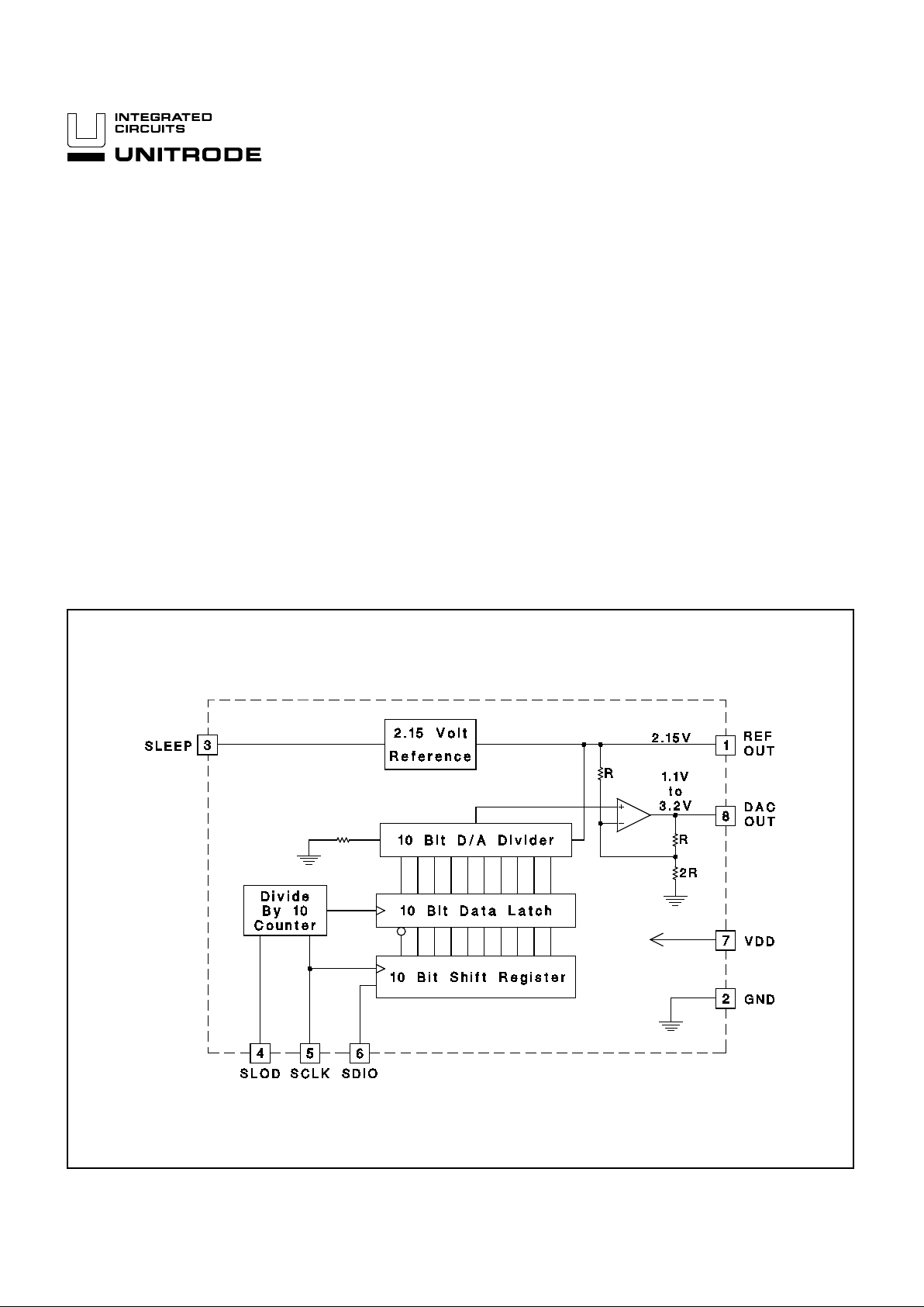
BLOCK DIAGRA M
2/95
FEATURES
• 10 Bit Resolution
• 1.1µs Output Rise Time
• 2.5µs Settling Time to 1%
• Single +5V Supply
• Monotonic
• Low Power Sleep Mode
• Three-wire Serial Interface
• 20MHz Data Rate
• 8 Pin SOIC and DIL Package
DESCRIPT IO N
The UCC5950 is a self-contained, microprocessor-compatible 10-bit D/A converter. It contains all of the functions required to take data directly from a threewire serial da ta bus and convert it to a preci se vol tage, i ncludi ng: an input shift
register, data latches, a p recisi on vo ltage reference, a precision 10-bit digital to
analog converter , and an output buffer amplifier.
The serial data interface i s cap able o f clo c k frequ enci es as hi gh as 20MHz, allowing update rates as high as two words per microsecond. The UCC5950 accepts commands encoded as 2’s-complement binary.
The data converter in the UCC5950 is inherently monotonic, making this part
ideal for use in closed-loop servo control systems as well as open-loop data
conversion. The UCC5950 uses a un ique segmented data converter which offers differential linea rity better than 1 LSB, integral linearity better than 2 LSB,
and fast conversion.
UCC5950
10-Bit Serial D/A Converter
UDG-95034
ABSOLUTE MAXIMUM RATINGS
VDD Supply Voltage. . . . . . . . . . . . . . . . . . . . . . . . . . . . . . . 6.5V
Input Voltage, Any I nput. . . . . . . . . . . . . . . . –0.3V to VDD+0.3V
Output Cur rent, Any Output . . . . . . . . . . . . . . . . . . . . . . . . ±5mA
Operating Tempe ratur e . . . . . . . . . . . . . . . . . . −55°C to +150°C
Stora g e Temperature. . . . . . . . . . . . . . . . . . . . −65°C to +150°C
Lead Temperature . . . . . . . . . . . . . . . . . . . . . . . . . . . . . . . 300°C
All voltages with respect to GND. All current s are positive int o,
negative out of, the sp ecifie d terminal. Consult Packa ging Section of Databook for thermal limitations and conside rations of
packages.
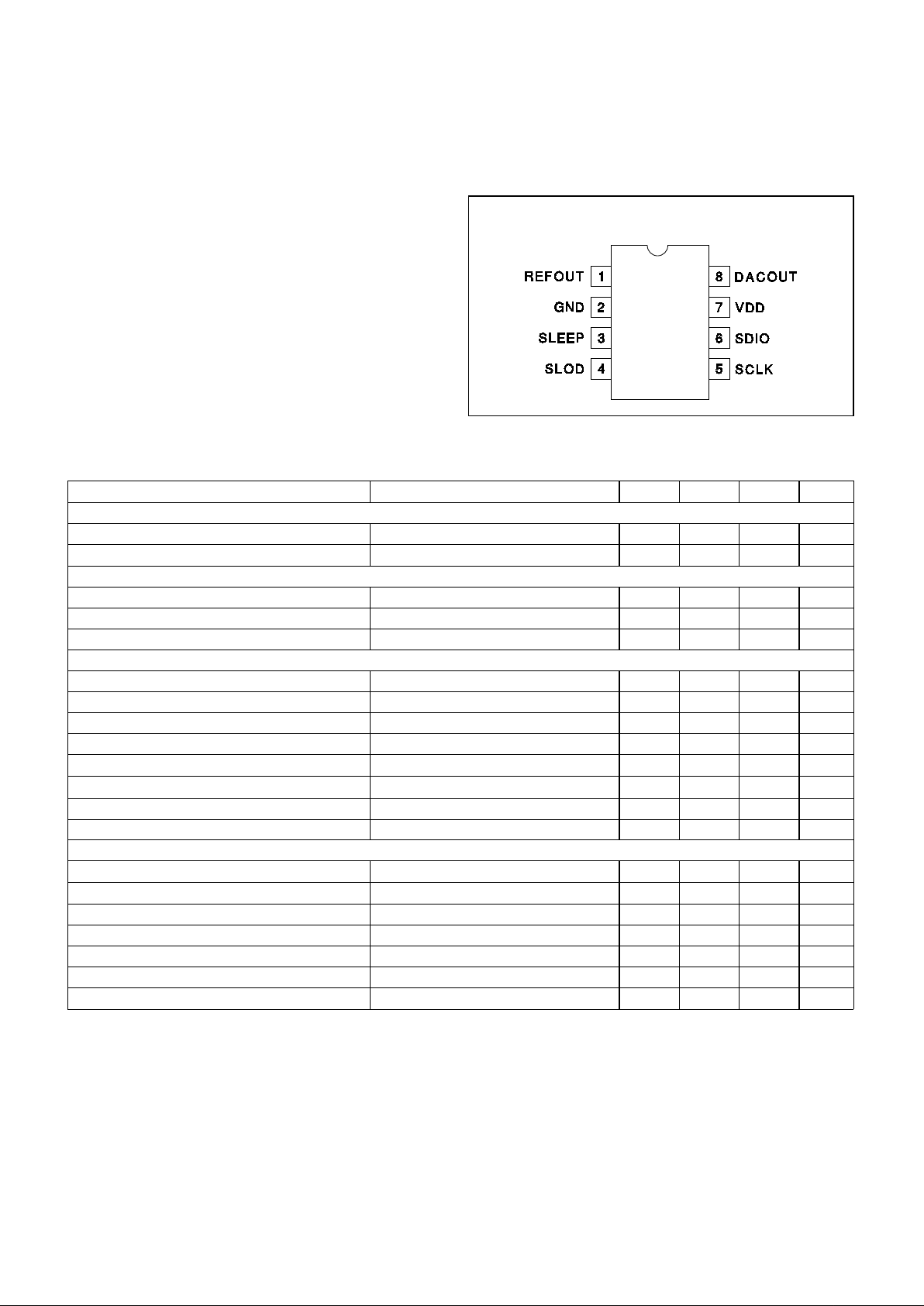
CONNECTION DIAG RAM
UCC5950
ELECTRICAL CHARACTERIST ICS Unless otherw ise stated, al l specificatio ns apply for 4.5V < VDD < 5.5V, REFOUT
Load < 100pF, DACOUT Load < 100pF, 0°C < T
A < +70°C, and TA = TJ.
PARAMETER TEST CONDITIONS MIN. TYP. MAX. UNITS
OVERALL SECTION
Supply Curren t SLEEP = 0V 1.5 5 mA
Supply Curren t SLEEP = 5V 0.1 10
µA
REFERENCE SECTION
REFOUT Output Volta ge 2.10 2.15 2.20 V
REFOUT Change with VDD 4.5V < VDD < 5.5V 1 10 mV
REFOUT Change with Load –1mA < I
REFOUT < 1mA 1 10 mV
D/A SECTION
Integral Nonlinearity (Note 1) 2 LSB
Differe ntial Nonlin earity 1 LSB
Full Scale Differe nce f ro m 1.49 24 x RE F –8 8 LSB
Zero Scale D ifference from 0.5089 x REF –8 8 LSB
DACOUT Full Scale Rise/Fall Time From 10% to 90% of swing (Note 4) 0.7 1.1
µs
DACOUT Full Scale Settling Time (TS) (Note 2, 3, 4) 1.4 2.5
µs
DACOUT Change with VDD 4.5V < VDD < 5.5V 1.5 10 mV
DACOUT Change with Load –1mA < I
DACOUT < 1mA 1.2 10 m V
LOGIC SECTION
Logic Input Thr esh old 1.5 2.5 3.5 V
Logic Input Cur ren t 0V < V
IN < VDD 5
µA
Logic Input Capacita nce (Note 4) 2.7 10 pF
SLOD Setup Time to SCLK low (TSLS) (Note 4) 50 ns
SLOD Hold Time from SCLK high (TSLH) From 10
TH
SCLK high (Note 4) 50 ns
SDIO Setup Time to SCLK high (TDS) (Note 4) 15 ns
SDIO Hold Time from SCLK high (TDH) (Note 4) 7 ns
Note 1: Integral nonlinear ity is defined as the worst deviat ion of the conve rter out put from th e best-fit straigh t line thro ugh
all converter ou tp ut codes.
Note 2: From 10
TH
Rising Edge of SCLK.
Note 3: Settling time is to 1% of final value.
Note 4: Guaranteed by design. Not 100% tested in production.
DIL-8, SOIC-8 (Top View)
N or J, D Package
2

UCC5950
DACOUT Falling Full Scale Step Response
REFOUT vs Temperatur e Supply Current vs Temperatu re
DACOUT Rising Full Scale Step Response
Logic Input Threshold vs Tempe rature DACOUT Change with DACOUT Load Current
TYPICAL CHARACTERISTICS
3

UCC5950
UNITRODE INTEGRA TED CIRCUITS
7 CONTINENTA L BLVD. • MERRIMACK, NH 03054
TEL. (603) 424-2410 • FAX (603) 424-3460
SLOD Internal Flag SCLK SDIO Internal Count Action DACOUT
11
don’t care don’t care
0
no actio n
V(t)
0 0 rising edge
DATA <10 Shift In DATA V(t)
0 0 rising edge
DATA 10 Latch New DATA
Set Internal Flag
Reset Count
V(t+1)
01
don’t care don’t care
0
no actio n
V(t)
SERIAL DATA INTERFACE TIMING AND LOGIC TABLE
PIN DESCRIPTIONS
DACOUT: The output of the 10-bit D/A Converter. For
best settling time, minimize load capacitance.
DACOUT will go to a voltage between 1.094V and
3.208V depending on the digital code loaded into the
latches. The digital code follows this pattern:
Input Code Typical DACOUT Significance
1000000000 1.094V Ze ro Scale
1000000001 1.096V
1000000010 1.098V
...
1111111111 2.151V
0000000000 2.153V Mid Scale
0000000001 2.155V
...
0111111110 3.206V
0111111111 3.208V Full Scale
GND: All signals are referenced to GND.
REFOUT: The output of the temperature-compensated
2.15V reference.
DO NOT BYPASS REFOUT!
For best
stability and transient response, minimize capacitance on
REFOUT.
SCLK: Data is clocked into the D/A after SLOD goes low
on rising edges of SCLK. A fter 10 rising edges of SCLK,
the data is latched into the D/A output register and the
outpu t i s updated. Further cl ock signals on SCLK are ignored until SLOD initiates a new read cycle.
SDIO: After SLOD goes low, data is clocked into the D/A
from the SDIO input, on ri sing e dges of SC LK, LSB first.
After 10 rising edges, da ta is latched and converted, and
further SCLK and SDIO information is ignored.
SLEEP: SLEEP is the power-down input to the D/A. In
systems not requiring this function, wire SLEEP to GND.
SLOD : SLOD is the chip-select input to the UCC5950.
SLOD going low selects the D/A and enables clocking of
data from SDIO into the D/A. After 10 SCLK pulses, the
D/A is updated and SLOD is ignored until SLOD goes
high and again goes low .
VDD: All an alog and digital functions are powered from
VDD. VDD should be a well-regulated supply to minimize
output variations. Bypass VDD to GND with a ceramic
capacitor very close to the UCC5950.
UDG-95035
4

IMPORTANT NOTICE
T exas Instruments and its subsidiaries (TI) reserve the right to make changes to their products or to discontinue
any product or service without notice, and advise customers to obtain the latest version of relevant information
to verify, before placing orders, that information being relied on is current and complete. All products are sold
subject to the terms and conditions of sale supplied at the time of order acknowledgement, including those
pertaining to warranty, patent infringement, and limitation of liability.
TI warrants performance of its semiconductor products to the specifications applicable at the time of sale in
accordance with TI’s standard warranty. Testing and other quality control techniques are utilized to the extent
TI deems necessary to support this warranty. Specific testing of all parameters of each device is not necessarily
performed, except those mandated by government requirements.
CERT AIN APPLICATIONS USING SEMICONDUCTOR PRODUCTS MAY INVOLVE POTENTIAL RISKS OF
DEATH, PERSONAL INJURY, OR SEVERE PROPERTY OR ENVIRONMENTAL DAMAGE (“CRITICAL
APPLICATIONS”). TI SEMICONDUCTOR PRODUCTS ARE NOT DESIGNED, AUTHORIZED, OR
WARRANTED TO BE SUITABLE FOR USE IN LIFE-SUPPORT DEVICES OR SYSTEMS OR OTHER
CRITICAL APPLICATIONS. INCLUSION OF TI PRODUCTS IN SUCH APPLICA TIONS IS UNDERSTOOD T O
BE FULLY AT THE CUSTOMER’S RISK.
In order to minimize risks associated with the customer’s applications, adequate design and operating
safeguards must be provided by the customer to minimize inherent or procedural hazards.
TI assumes no liability for applications assistance or customer product design. TI does not warrant or represent
that any license, either express or implied, is granted under any patent right, copyright, mask work right, or other
intellectual property right of TI covering or relating to any combination, machine, or process in which such
semiconductor products or services might be or are used. TI’s publication of information regarding any third
party’s products or services does not constitute TI’s approval, warranty or endorsement thereof.
Copyright 1999, Texas Instruments Incorporated
 Loading...