

UCC5639
Multimode SCSI 15 Line Terminator with Reverse Disconnect
FEATURES
• Auto Selection Single Ended (SE) or
Low Voltage Differential (LVD)
Termination
• Meets SCSI-1, SCSI-2, SCSI-3, SPI,
Ultra (Fast-20), Ultra2 (SPI-2 LVD)
and Ultra3 Standards
• 2.7V to 5.25V Operation
• Differential Failsafe Bias
• Thermal packaging for low junction
temperature and better MTBF.
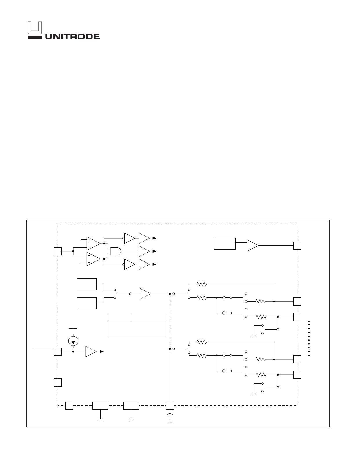
BLOCK DIAGRAM
2.05V
34DIFFB
0.6V
DESCRIPTION
The UCC5639 Multimode SCSI Terminator provides a smooth transition
into the next generation of the SCSI Parallel Interface (SPI-2). It automatically senses the bus, via DIFFB, and switches the termination to either single ended (SE) or low voltage differential (LVD) SCSI, dependent on which
type of devices are connected to the bus. The UCC5639 can not be used
on a HVD, EIA485, differential SCSI bus. If the UCC5639 detects a HVD
SCSI device, it switches to a high impedance state.
The Multimode terminator contains all functions required to terminate and
auto detect and switch modes for SPI-2 bus architectures. Single Ended
and Differential impedances and currents are trimmed for maximum effectiveness. Fail Safe biasing is provided to insure signal integrity. Device/Bus
type detection circuitry is integrated into the terminator to provide automatic
switching of termination between single ended and LVD SCSI and a high
impedance for HVD SCSI. The multimode function provides all the performance analog functions necessary to implement SPI-2 termination in a single monolithic device.
The UCC5639 is offered in a 48 pin LQFP package for a temperature range
of 0°C to 70°C.
HIGH PO WER
DIFFERENTIAL
LOW VOLT AGE
DIFFERENTIAL
SINGLE ENDED
(NOISE LOAD)
REF
1.3V
–15mA ≤ I
50µA ≤ I
SOURCE
SINK
≤ –5mA
≤ 200µA
1.3V
35 DIFFSENS
DISCNCT
03/99
REF
2.7V
REF
1.25V
36
3TRMPWR
HS/GND
27
GND
4-9
SOURCE/SINK REGULATOR
MODE
DISCNCT
SE
LVD
HS/GND
ALL SWITCHES
UP
DOWN
OPEN
28-33
REG
10
4.7µF .
110
124
110
124
56mV
–+
56mV
+–
SE GND SWITCH
56mV
–+
56mV
+–
SE GND SWITCH
52.5
52.5
52.5
52.5
12
11
2
1
L1–
L1+
L15–
L15+
UDG-98110
UCC5639
ABSOLUTE MAXIMUM RATINGS
TRMPWR Voltage. . . . . . . . . . . . . . . . . . . . . . . . . . . . . . . . +6V
Signal Line Voltage . . . . . . . . . . . . . . . . . . . . . 0V to TRMPWR
Package Dissipation. . . . . . . . . . . . . . . . . . . . . . . . . . . . . . . 2W
Storage Temperature . . . . . . . . . . . . . . . . . . . –65°C to +150°C
Junction Temperature. . . . . . . . . . . . . . . . . . . –55°C to +150°C
Lead Temperature (Soldering, 10 sec.). . . . . . . . . . . . . +300°C
Recommended Operating Conditions . . . . . . . . . 2.7V to 5.25V
Currents are positive into negative out of the specified terminal.
Note: Consult Packaging Section of Databook for thermal limitations and considerations of package.
RECOMMENDED OPERATING CONDITIONS
TRMPWR Voltage . . . . . . . . . . . . . . . . . . . . . . . . 2.7V to 5.25V
Temperature Ranges . . . . . . . . . . . . . . . . . . . . . . 0°C to +70°C
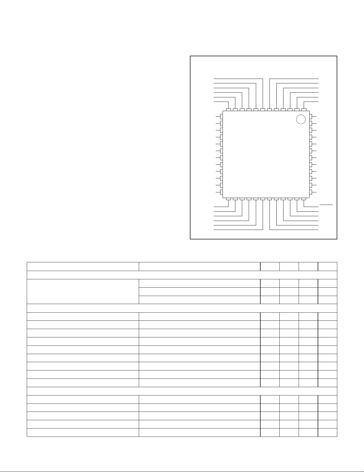
CONNECTION DIAGRAMS
(TOP VIEW)
FQP Package
HS/GND
HS/GND
HS/GND
REG
L1+
L1–
12
10
L8+
GND
HS/GND
HS/GND
HS/GND
L8–
L2+
L2–
L3+
L3–
L4+
L4–
L5+
L5–
L6+
L6–
L7+
L7–
11
13
14
15
16
17
18
19
20
21
22
23
24
25
26
8
7
9
27
29
30
28
6
5
313233
HS/GND
HS/GND
HS/GND
TRMPWR
L15–
L15+
2
4
3
1
L14–
48
47
L14+
L13–
46
L13+
45
L12–
44
L12+
43
L11–
42
L11+
41
L10–
40
L10+
39
38
L9–
37
35
34
L9+
36
DISCNCT
DIFSENS
DIFFB
HS/GND
HS/GND
HS/GND
ELECTRICAL CHARACTERISTICS
Unless otherwise stated, these specifications apply for TA= TJ= 0°C to 70°C,
TRMPWR = 3.3V.
PARAMETER TEST CONDITIONS MIN TYP MAX UNITS
TRMPWR Supply Current Section
TRMPWR Supply Current LVD Mode 20 25 mA
SE Mode 1.6 10 mA
Disabled Terminator 250 400
Regulator Section
1.25V Regulator LVD Mode 1.15 1.25 1.35 V
1.25V Regulator Source Current V
1.25V Regulator Sink Current V
= 0V –375 –700 –1000 mA
REG
= 3.3V 170 300 700 mA
REG
1.3V Regulator DIFSENS 1.2 1.3 1.4 V
1.3V Regulator Source Current V
1.3V Regulator Sink Current V
= 0V –15 –5 mA
REG
= 3.3V 50 200 µA
REG
2.7V Regulator SE Mode 2.5 2.7 3.0 V
2.7V Regulator Source Current V
2.7V Regulator Sink Curren V
= 0V –375 –700 –1000 mA
REG
= 3.3V 170 300 700 mA
REG
Differential Termination Section
Differential Impedance 100 105 110 Ω
Common Mode Impedence (Note 2) 110 150 165 Ω
Differential Bias Voltage 100 125 mV
Common Mode Bias 1.15 1.25 1.35 V
Output Capacitance Single Ended Measurement to Ground (Note 1) 3 pF
µA
2

UCC5639
ELECTRICAL CHARACTERISTICS Unless otherwise stated, these specifications apply for T
TRMPWR = 3.3V.
PARAMETER TEST CONDITIONS MIN TYP MAX UNITS
Single Ended Termination Section
Impedance
Termination Current Signal Level 0.2V, All Lines Low –21 –24 –25.4 mA
Output Leakage 400 nA
Output Capacitance Single Ended Measurement to Ground (Note 1) 3 pF
Single Ended GND SE Impedance I= 10mA 20 60
Disconnect and Diff Buffer Input Section
DISCNCT
DISCNCT
Diff Buffer Single Ended to LVD Threshold 0.5 0.7 V
Diff Buffer LVD to HPD Threshold 1.9 2.2 V
DIFFB Input Current –10 10
Note 1: Guaranteed by design. Not 100% tested in production.
Note 2:
Threshold 0.8 2.0 V
Input Current 10 30 µA
12
.
Z
=
CM
II
[]
VCM V VCM V
(.)(.)
V
–
+−
06 06
where VCM=voltage measured with L+ tied to L– and zero current applied
VL V
−(.)02
X
Z
=
Signal Level 0.5V –18 –22.4 mA
IL
X
, (Note 3)
= TJ= 0°C to 70°C,
A
102.3 110 117.7
Ω
Ω
µA
Note 3: VL
= Output voltage for each terminator minus output pin (L1– through L15–) with each pin unloaded.
X
= Output current for each terminator minus output pin (L1– through L15–) with the minus output pin forced to 0.2V.
IL
X
PIN DESCRIPTIONS
DIFFB: Diff sense filter pin should be connected at a
0.1µF capacitor.
DIFFSENS: The SCSI bus Diff Sense line to detect what
types of devices are connected to the SCSI bus.
DISCNCT
when it is not at the end of the bus. The disconnect pin
high enables the terminator.
: Disconnect pin shuts down the terminator
LINE
n
–: Signal line active line for single ended or nega-
tive line in differential applications for the SCSI bus.
LINE
n
+: Ground line for single ended or positive line for
differential applications for the SCSI bus.
REG: Regulator bypass pin, must be connected to a
4.7µF capacitor.
TRMPWR: V
2.7V to 5.25V supply.
IN
3

APPLICATION INFORMATION
The UCC5639 is a Multi-mode active terminator with selectable single ended (SE) and low voltage differential
(LVD) SCSI termination integrated into a monolithic component. Mode selection is accomplished with the “diff
sense" signal.
The diff sense signal is a three level signal, which is
driven at each end of the bus by one active terminator. A
LVD or multi-mode terminator drives the diff sense line to
1.3 V. If diff sense is at 1.3 V, then bus is in LVD mode. If
a single ended SCSI device is plugged into the bus, the
diff sense line is shorted to ground. With diff sense
shorted to ground, the terminator changes to single
ended mode to accommodate the SE device. If a HVD
device is plugged in to the bus, the diff sense line is
pulled high and the terminator shuts down.
The diff sense line is driven and monitored by the terminator through a 50Hz noise filter at the DIFFB input pin.
A set of comparators, that allow for ground shifts, determine the bus status as follows. Any diff sense signal below 0.5V is single ended, between 0.7V and 1.9V is LVD
and above 2.2V is HVD.
In the single ended mode, a multi-mode terminator has a
110Ω terminating resistor connected to a 2.7V termination voltage regulator. The 2.7V regulator is used on all
Unitrode terminators designed for 3.3V systems. This requires the terminator to operate in specification down to
2.7V TRMPWR voltage to allow for the 3.3V supply tolerance, an unidirectional fusing device and cable drop. At
each L+ pin, a ground driver drives the pin to ground,
while in single ended mode. The ground driver is specially designed so it will not effect the capacitive balance
of the bus when the device is in LVD or disconnect mode.
The device requirements call for 0.5pF balance on the
lines of a differential pair. The terminator capacitance has
to be a small part of the capacitance imbalance.
Layout is very critical for Ultra2 and Ultra3 systems.
Multi-layer boards need to adhere to the 120Ω impedance standard, including connector and feed-through.
This is normally done on the outer layers with 4 mil etch
UCC5639
and 4 mil spacing between the runs within a pair, and a
minimum of 8 mil spacing to the next pair. This spacing
between the pairs reduces potential crosstalk. Beware of
feed-throughs and each through hole connection adds a
lot of capacitance. Standard power and ground plane
spacing yields about 1pF to each plane. Each feedthrough will add about 2.5pF to 3.5pF. Enlarging the
clearance holes on both power and ground planes can
reduce the capacitance and opening up the power and
ground planes under the connector can reduce the capacitance for through hole connector applications. Microstrip technology is normally too low of impedance and
should not be used. It is designed for 50Ω rather than
120Ω differential systems.
Capacitance balance is critical for Ultra2 and Ultra3. The
balance capacitance standard is 0.5pF per line with the
balance between pairs of 2pF. The components are designed with very tight balance, typically 0.1pF between
pins in a pair and 0.3pF between pairs. Layout balance is
critical, feed-throughs and etch length must be balanced,
preferably no feed-throughs would be used. Capacitance
for devices should be measured in the typical application,
material and components above and below the circuit
board effect the capacitance.
Multi-mode terminators need to consider power dissipation; the UCC5639 is offered in a power package with
heat sink ground pins. These heat sink/ground pins are
directly connected to the die mount paddle under the die
and conduct heat from the die to reduce the junction
temperature. These pins need to be connected to etch
area or a feed-through per pin connecting to the ground
plane layer on a multi-layer board.
In 3.3V TRMPWR systems, the UCC3912 should be
used to replace the fuse and diode. This reduces the
voltage drop, allowing for cable drop to the far end terminator. 3.3V battery systems normally have a 10% tolerance. The UCC3912 is 150mV drop under LVD loads,
allowing 150mV drop in the cable system. All Unitrode
LVD and multi-mode terminators are designed for 3.3V
systems, operating down to 2.7V.
4

TYPICAL APPLICATION
UCC5639
4.7µF
3
36
TRMPWR
DISCNCT
REG
DATALINES (15)
DIFFB REGDIFFB
10 34
4.7µF
.
L1+
L1–
L9+
L9–
L10+
L10–
L13+
L13–
L1+
L1–
L5+
L5–
35
0.1µF
.
CONTROL LINES (9)
4 BITS OF THE HIGH BYTE
DIFF SENSE
20k
220k
HIGH BYTE 4 BITS
PLUS P ARITY
20k
L1+
L1–
L9+
L9–
L10+
L10–
L13+
L13–
35
DIFSENSDIFSENS
34 10
L1+
L1–
DATALINES (15)
L5+
L5–
0.1µF
.
TRMPWR
DISCNCT
3
36
4.7µF
Termp owerTermp ower
4.7µF
.
TRMPWR
3
36
DISCNCT
REG
10 34
SCSI CONTROLLER
DIFFSENS
4.7µF
.
L14+
L14–
DIFFB
L6+
L6–
L6+
L6–
LOW BYTE 8+ PARITY
L14+
L14–
34 10
TRMPWR
DISCNCT
REGDIFFB
3
36
4.7µF
UDG-98111
Note: A 220k resistor is added to ground to insure the transceivers will come up in single-ended mode when no terminator is enabled.The controller DIFFSENS ties to the DIFFB pin on the terminators, only one RC network should be on a device.
UNITRODE CORPORATION
7 CONTINENTAL BLVD.• MERRIMACK, NH 03054
TEL. (603) 424-2410 • FAX (603) 424-3460
5

IMPORTANT NOTICE
T exas Instruments and its subsidiaries (TI) reserve the right to make changes to their products or to discontinue
any product or service without notice, and advise customers to obtain the latest version of relevant information
to verify, before placing orders, that information being relied on is current and complete. All products are sold
subject to the terms and conditions of sale supplied at the time of order acknowledgement, including those
pertaining to warranty, patent infringement, and limitation of liability.
TI warrants performance of its semiconductor products to the specifications applicable at the time of sale in
accordance with TI’s standard warranty. T esting and other quality control techniques are utilized to the extent
TI deems necessary to support this warranty . Specific testing of all parameters of each device is not necessarily
performed, except those mandated by government requirements.
CERTAIN APPLICATIONS USING SEMICONDUCTOR PRODUCTS MAY INVOL VE POTENTIAL RISKS OF
DEATH, PERSONAL INJURY, OR SEVERE PROPERTY OR ENVIRONMENTAL DAMAGE (“CRITICAL
APPLICATIONS”). TI SEMICONDUCTOR PRODUCTS ARE NOT DESIGNED, AUTHORIZED, OR
WARRANTED TO BE SUITABLE FOR USE IN LIFE-SUPPORT DEVICES OR SYSTEMS OR OTHER
CRITICAL APPLICA TIONS. INCLUSION OF TI PRODUCTS IN SUCH APPLICATIONS IS UNDERST OOD TO
BE FULLY AT THE CUSTOMER’S RISK.
In order to minimize risks associated with the customer’s applications, adequate design and operating
safeguards must be provided by the customer to minimize inherent or procedural hazards.
TI assumes no liability for applications assistance or customer product design. TI does not warrant or represent
that any license, either express or implied, is granted under any patent right, copyright, mask work right, or other
intellectual property right of TI covering or relating to any combination, machine, or process in which such
semiconductor products or services might be or are used. TI’s publication of information regarding any third
party’s products or services does not constitute TI’s approval, warranty or endorsement thereof.
Copyright 1999, Texas Instruments Incorporated
 Loading...