

UCC5630
01/99
FEATURES
• Auto Selection Multi-Mode Single
Ended or Low Voltage Differential
Termination
• 2.7V to 5.25V Operation
• Differential Failsafe Bias
• Thermal Packaging for Low Junction
Temperature and Better MTBF
• Master/Slave Inputs
• Supports Active Negation
• Standby (Disable Mode) 5µA
• 3pF Channel Capacitance
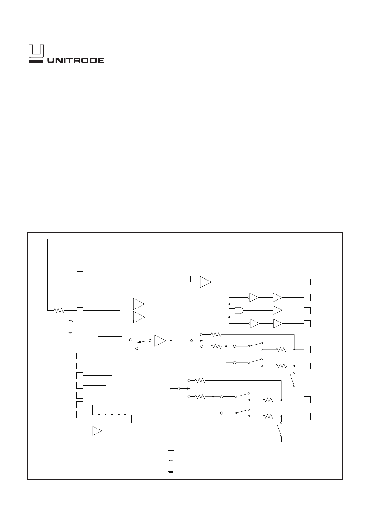
Low Voltage Differential (LVD/SE) SCSI 9 Line Terminator
8HS/GND
1
REG
DIFFSENS
5 L1–
4 L1+
32 L9–
31 L9+
125
+50mV TO +62.5mV
SWITCHES UP ARE SINGLE
ENDED SWITCHES DOWN ARE
LOW VOLTAGE DIFFERENTIAL
0.7 > 0.6V
2.2 > 1.9V
SE GND
SWITCH
52
110
52
125
+50mV TO +62.5mV
52
110
52
21
DIFFB
REF 2.7V
REF 1.25V
9
10
26
27
28
18
HS/GND
HS/GND
HS/GND
HS/GND
HS/GND
GND
19MSTR/SLV
36TRMPWR
+V
DD
REEF 1.3V
1.3V ± –0.1V
20
SOURCE 5 < 15mA
SINK 200µAMAXIMUM(NOISELOAD)
34 LVD
33 SE
35
HIPD
0.1µF
20k
LOW
FREQUENCY
FILTER
50Hz – 60Hz
SOURCE ONLY FROM TRMPWR AND THE ENABLED TERMINATORS
OPEN CIRCUIT ON POWER OFF
OR
OPEN CIRCUIT IN A DISABLED
TERMINATOR MODE
SOURCE/SINK
REGULATOR
HIGH IMPEDANCE
RECEIVER EVEN
WITH POWER OFF
17DISCNCT
4.7µF
MWP 36 PINOUT
BLOCK DIAGRAM
UDG-98049
DESCRIPTION
The UCC5630 Multi-Mode Low Voltage Differential and Single Ended Terminator is both a single ended terminator and a low voltage differential terminator for the transition to the next generation SCSI Parallel Interface
(SPI-2). The low voltage differential is a requirement for the higher speeds
at a reasonable cost and is the only way to have adequate skew budgets.
The transceivers can be incorporated into the controller, unlike SCSI high
power differential (EIA485) which requires external transceivers. Low Voltage differential is specified for Fast-40 and Fast-80, but has the potential of
speeds up to Fast-320. The UCC5630 is SPI-2, SPI and Fast-20 compliant.
Consult SSOP-36 and LQFP-48 Package Diagram for exact dimensions.
The UCC5630 can not be used with SCSI high voltage differential (HVD)
EIA485. It will shut down when it sees high power differential to protect the
bus. The pinning for high power differential is not the same as LVD or single ended and the bias voltage, current and power are also different for
EIA485 differential.
Circuit Design Patented
2
UCC5630
L3+
HS/GND
L9–
L9+
L8–
TRMPWR
N/C
N/C
HS/GND
L2–
HS/GND
L1+
L1–
L2+
REG
HS/GND
L3–
L8+
HS/GND
HS/GND
L4+
L4–
14
13
12
11
10
9
8
7
6
5
4
3
2
1
23
24
25
26
27
28
29
30
31
32
33
34
35
36
18
17
16
15
DIFF B
MSTR/SLV
DIFSENS
19
20
21
22L5+
L5–
DISCNCT
GND
L7–
L7+
L6–
L6+
HIPD
LVD
SE
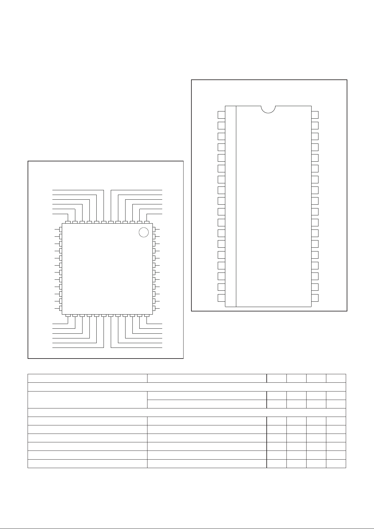
CONNECTION DIAGRAM
SSOP-36 (Top View)
MWP Package
ABSOLUTE MAXIMUM RATINGS
TRMPWR Voltage. . . . . . . . . . . . . . . . . . . . . . . . . . . . . . . . . 6V
Signal Line Voltage . . . . . . . . . . . . . . . . . . . . . 0V to TRMPWR
Package Power Dissipation . . . . . . . . . . . . . . . . . . . . . . . . . 2W
Storage Temperature . . . . . . . . . . . . . . . . . . . –65°C to +150°C
Junction Temperature. . . . . . . . . . . . . . . . . . . –55°C to +150°C
Lead Temperature (Soldering, 10sec.) . . . . . . . . . . . . . +300°C
All voltages are with respect to PIN1.Currents are positive into,
negative out of the specified terminal. Consult Packaging Section of the Databook for thermal limitations and considerations
of packages.
12
11
10
9
13
8
7
6
5
4
3
2
1
14
15
16
17
18
19
20
21
22
23
24
25
26
27
28
29
30
313233
34
35
36
48
47
46
45
44
43
42
41
40
39
38
37
MSTR/SLV
DIFSENS
DIFFB
N/C
HS GND
HS GND
L7–
L7+
L6–
L6+
HS/GND
HS/GND
HS/GND
L5+
L5–
DISCNCT
GND
HS/GND
HS/GND
L4+
L4–
L3+
L3–
NC
L2+
L2–
L1+
L1–
HS/GND
HS/GND
NC
REG
NC
NC
HS/GND
HS/GND
HS/GND
L9–
L9+
L8–
L8+
HS/GND
HS/GND
LVD
SE
TERMPWR
HIPD
NC
LQFP-48 (Top View)
FQP Package
RECOMMENDED OPERATING CONDITIONS
TRMPWR Voltage . . . . . . . . . . . . . . . . . . . . . . . 2.7V TO 5.25V
ELECTRICAL CHARACTERISTICS: Unless otherwise specified, T
A
= 0°C to 70°C, TRMPWR = 3.3V.
PARAMETER TEST CONDITIONS MIN TYP MAX UNITS
TRMPWR Supply Current Section
TRMPWR Supply Current 20 mA
Disable Terminator, in DISCNCT mode. 35 µA
Regulator Section
1.25V Regulator LVD Mode 1.15 1.25 1.35 V
1.25V Regulator Source Current LVD Mode, Differential Sense Floating –80 –100 mA
1.25V Regulator Sink Current LVD Mode, Differential Sense Floating 80 100 mA
1.3V Regulator DIFSENS 1.2 1.3 1.4 V
1.3V Regulator Source Current DIFSENS –5 –15 mA
1.3V Regulator Sink Current DIFSENS 50 200 µA

3
UCC5630
ELECTRICAL CHARACTERISTICS: Unless otherwise specified, T
A
= 0°C to 70°C, TRMPWR = 3.3V.
PARAMETER TEST CONDITIONS MIN TYP MAX UNITS
2.7V Regulator Single Ended Mode 2.5 2.7 3 V
2.7V Regulator Source Current Single Ended Mode –200 –400 –800 mA
2.7V Regulator Sink Current Single Ended Mode 100 200 400 mA
2.7V Regulator Dropout Voltage V
TRMPWR
– (V
REG
– 2.7 Min) 200 mV
Differential Termination Section
Differential Impedance 100 105 110 Ω
Common Mode Impedance 110 125 165 Ω
Differential Bias Voltage Drivers Tri-stated 100 125 mV
Common Mode Bias 1.25 V
Output Capacitance Single Ended Measurement to Ground (Note 1) 3.5 pF
Single Ended Termination Section
Impedance 102.3 110 117.7 Ω
Termination Current Signal Level 0.2V –21 –23 –25.4 mA
Signal Level 0.5V –22.4 mA
Output Leakage Disabled, TRMPWR = 0V to 5.25V 400 nA
Output Capacitance Single Ended Measurement to Ground (Note 1) 3 pF
Single Ended GND SW Impedance 60 Ω
Disconnect (DISCNCT) Input Section
DISCNCT Threshold 0.8 2.0 V
DISCNCT Input Current V
DISCNCT
= 0V and 3.3V –30 30 µA
Differential Sense (DIFFB) Input Sections
DIFFB Single Ended Threshold 0.6 0.7 V
DIFFB Sense LVDS Threshold 1.9 2.2 V
DIFFB Input Current V
DIFFB
= 0V and 3.3V –30 30 µA
Master/Slave (MSTR/SLV) Input Section
MSTR/SLV Threshold 0.8 2 V
MSTR/SLV Input Current –30 30 µA
Status Bits (SE, LVD, HIPD) Output Section
I
SOURCE
V
LOAD
= 2.4V –4 –8.7 mA
I
SINK
VLOAD = 0.5V 3 6 mA
V
LOAD
= 0.4V 2 5 mA
Note 1: Guaranteed by design. Not 100% tested in production.
PIN DESCRIPTIONS
DIFFB: DIFSENS filter pin should be connected to a
0.1µF capacitor to GND and 20k resistor to SCSI/Bus
DIFSENS Line.
DIFSENS: The SCSI bus DIFSENS line is driven to 1.3V
to detect what type of devices are connected to the SCSI
bus.
DISCNCT: Disconnect shuts down the terminator when it
is not at the ended of the bus. The disconnect pin low enables the terminator.
HIPD: TTL compatible status bit indicating high voltage
differential has been detected on DIFFB. The terminator
is in shutdown. (Not valid in disconnect mode.)
HS/GND: Heat Sink GND. Connect to large area PC
board traces to increase power dissipation capability.
GND: Power Supply Return.
L1– thru L9–: Signal line/active line for single ended or
negative line in differential applications for the SCSI bus.
L1+ thru L9+: Ground line for single ended or positive
line for differential applications for the SCSI bus.
LVD: TTL compatible status bit indicating low voltage dif-
ferential level on DIFFB. The terminator is in LVD
mode.(Not valid in disconnect mode.)

4
UCC5630
UNITRODE CORPORATION
7 CONTINENTAL BLVD.• MERRIMACK, NH 03054
TEL. (603) 424-2410 • FAX (603) 424-3460
REG
TERMPWR
DISCNCT
TERMPWR
DIFFB REGDIFF B
TERMPWRTERMPWR
4.7
µF .
4.7µF . 0.1µF . 4.7µF0.1µF .
36
17
20
1 21
20k
20
21 1
CONTROL LINES
36
DISCNCT
17
CONTROL LINES
DIFFSENSEDIFFSENSE
REG
TERMPWR
DISCNCT
DIFF B
4.7µF .
36
17
1 21
DATA LINES (9)
20k
REG
TERMPWR
DIFFB
4.7µF .
36
19
1 21
DATA LINES (9)
TERMPWR
REGDIFFB
4.7µF
21 1
DATA LINES (9)
36
DISCNCT
17
TERMPWR
REGDIFFB
4.7µF
21 1
DATA LINES (9)
36
DISCNCT
17
4.7µF .
MSTR/SLV19 19MSTR/SLV
19MSTR/SLV
19MSTR/SLV
MSTR/SLV19
DISCNCT
17
MSTR/SLV
APPLICATION INFORMATION
UDG-96211
Balancing capacitor is very important in high speed operation. The typical balance between the positive (+) and
negative (–) signals is 0.1pF except for L8 and L9,
0.23pF and 0.4pF respecitvely on the MWP package.
The negative (–) signal has higher capacitance than the
positive (+) signal. The FQP package is typically 0.2pF
less than the MWP. Typical balance is 0.1pF except for
L8 and L3, where it is 0.4pF.
The master is selected by placing TRMPWR on
MSTR/SLV and the terminator enabled by grounding
DISCNCT, enabling the 1.3V regulator. The master is the
only terminator connected directly to DIFSENS bus line,
all the other terminators receive the mode signal by connecting the DIFFB pins together.
Note: The Master/Slave function will not be on future terminators.
MSTR/SLV: Mode select for the non-controlling terminator. MSTR enables the 1.3V regulator, when the terminator is enabled. Note: Theis function will be removed on
further generations of the multimode terminators.
REG: Regulator bypass, must be connected to a 4.7µF
capacitor.
SE: TTL compatible status bit indicating single ended de-
vice has been detected on DIFFB. The terminator is in
single ended mode.
TRMPWR: V
IN 2.7V to 5.25V supply.
PIN DESCRIPTIONS (cont.)

IMPORTANT NOTICE
T exas Instruments and its subsidiaries (TI) reserve the right to make changes to their products or to discontinue
any product or service without notice, and advise customers to obtain the latest version of relevant information
to verify, before placing orders, that information being relied on is current and complete. All products are sold
subject to the terms and conditions of sale supplied at the time of order acknowledgement, including those
pertaining to warranty, patent infringement, and limitation of liability.
TI warrants performance of its semiconductor products to the specifications applicable at the time of sale in
accordance with TI’s standard warranty. Testing and other quality control techniques are utilized to the extent
TI deems necessary to support this warranty. Specific testing of all parameters of each device is not necessarily
performed, except those mandated by government requirements.
CERT AIN APPLICATIONS USING SEMICONDUCTOR PRODUCTS MAY INVOLVE POTENTIAL RISKS OF
DEATH, PERSONAL INJURY, OR SEVERE PROPERTY OR ENVIRONMENTAL DAMAGE (“CRITICAL
APPLICATIONS”). TI SEMICONDUCTOR PRODUCTS ARE NOT DESIGNED, AUTHORIZED, OR
WARRANTED TO BE SUITABLE FOR USE IN LIFE-SUPPORT DEVICES OR SYSTEMS OR OTHER
CRITICAL APPLICATIONS. INCLUSION OF TI PRODUCTS IN SUCH APPLICA TIONS IS UNDERSTOOD T O
BE FULLY AT THE CUSTOMER’S RISK.
In order to minimize risks associated with the customer’s applications, adequate design and operating
safeguards must be provided by the customer to minimize inherent or procedural hazards.
TI assumes no liability for applications assistance or customer product design. TI does not warrant or represent
that any license, either express or implied, is granted under any patent right, copyright, mask work right, or other
intellectual property right of TI covering or relating to any combination, machine, or process in which such
semiconductor products or services might be or are used. TI’s publication of information regarding any third
party’s products or services does not constitute TI’s approval, warranty or endorsement thereof.
Copyright 1999, Texas Instruments Incorporated
 Loading...