

Multimode SCSI 14 Line Terminator
UCC5628
FEATURES
Auto Selection Single Ended (SE) or
•
Low Voltage Differential (LVD)
Termination
Meets SCSI-1, SCSI-2, SCSI-3, SPI,
•
Ultra (Fast-20), Ultra2 (SPI-2 LVD)
and Ultra3 Standards
2.7V to 5.25V Operation
•
Differential Failsafe Bias
•
Thermal packaging for low junction
•
temperature and better MTBF.
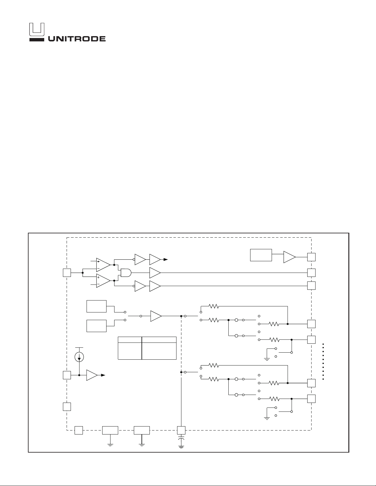
BLOCK DIAGRAM
2.15V
DESCRIPTION
The UCC5628 Multimode SCSI Terminator provides a smooth transition
into the next generation of the SCSI Parallel Interface (SPI-2). It automati
cally senses the bus, via DIFFB, and switches the termination to either sin
gle ended (SE) or low voltage differential (LVD) SCSI, dependent on which
type of devices are connected to the bus. The UCC5628 can not be used
on a HVD, EIA485, differential SCSI bus. If the UCC5628 detects a HVD
SCSI device, it switches to a high impedance state.
The Multimode terminator contains all functions required to terminate and
auto detect and switch modes for SPI-2 bus architectures. Single Ended
and Differential impedances and currents are trimmed for maximum effec
tiveness. Fail Safe biasing is provided to insure signal integrity. Device/Bus
type detection circuitry is integrated into the terminator to provide automatic
switching of termination between single ended and LVD SCSI and a high
impedance for HVD SCSI. The multimode function provides all the per
formance analog functions necessary to implement SPI-2 termination in a
single monolithic device.
The UCC5628 is offered in a 48 pin LQFP package for a temperature
range of 0°C to 70°C.
(NOISE LOAD)
HPD
–15mA ≤I
50µA ≤I
SOURCE
SINK
≤–5mA
≤200µA
REF
1.3V
1.3V
35 DIFFSEN
-
-
-
-
DISCNCT
34DIFFB
0.6V
REF
2.7V
REF
1.25V
10µA
36
3TRMPWR
HS/GND
25
GND
4-9
SOURCE/SINK REGULATOR
SE
LVD
HS/GND
ALL SWITCHES
UP
DOWN
OPEN
28-33
MODE
DISCNCT
10
REG
4.7µF .
110
124
110
124
56mV
–+
56mV
+–
SE GND SWITCH
56mV
–+
56mV
+–
SE GND SWITCH
52.5
52.5
52.5
52.5
27
LVD
SE
26
L1–
12
L1+
11
L14–
2
L14+
1
UDG-98099
SLUS302A - SEPTEMBER 1999
UCC5628
ABSOLUTE MAXIMUM RATINGS
TRMPWR Voltage . . . . . . . . . . . . . . . . . . . . . . . . . . . . . . . . +6V
Signal Line Voltage . . . . . . . . . . . . . . . . . . . . . 0V to TRMPWR
Package Dissipation . . . . . . . . . . . . . . . . . . . . . . . . . . . . . . . 2W
Storage Temperature . . . . . . . . . . . . . . . . . . . –65°C to +150°C
Junction Temperature. . . . . . . . . . . . . . . . . . . –55°C to +150°C
Lead Temperature (Soldering, 10 sec.) . . . . . . . . . . . . . +300°C
Recommended Operating Conditions . . . . . . . . . 2.7V to 5.25V
Currents are positive into negative out of the specified terminal.
Note: Consult Packaging Section of Databook for thermal limi
-
tations and considerations of package.
RECOMMENDED OPERATING CONDITIONS
TRMPWR Voltage . . . . . . . . . . . . . . . . . . . . . . . . 2.7V to 5.25V
Temperature Ranges . . . . . . . . . . . . . . . . . . . . . . 0°C to +70°C
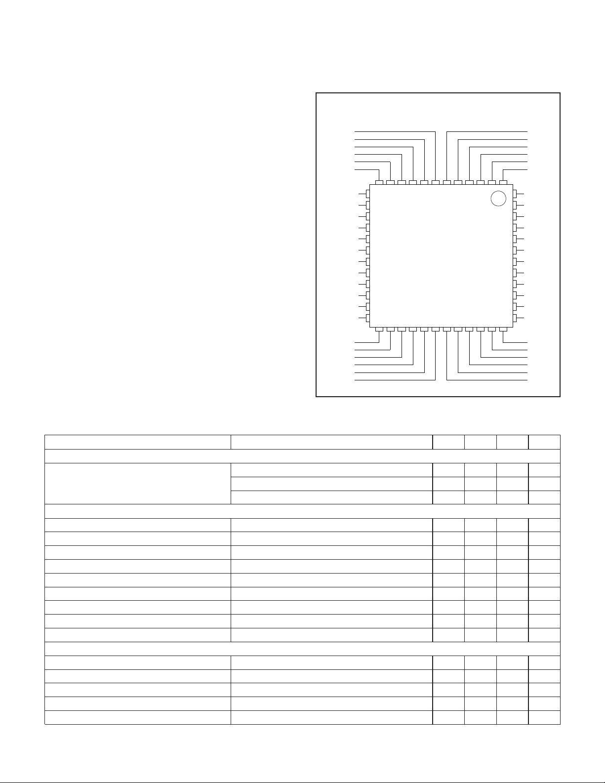
CONNECTION DIAGRAMS
(TOP VIEW)
FQP Package
HS/GND
HS/GND
HS/GND
REG
L1+
L1–
12
10
GND
LVD
HS/GND
HS/GND
HS/GND
L2+
L2–
L3+
L3–
L4+
L4–
L5+
L5–
L6+
L6–
L7+
L7–
SE
11
13
14
15
16
17
18
19
20
21
22
23
24
25
26
8
7
9
27
29
30
28
6
5
313233
HS/GND
HS/GND
HS/GND
TRMPWR
L14–
L14+
2
4
3
1
L13–
48
47
L13+
L12–
46
L12+
45
L11–
44
L11+
43
L10–
42
L10+
41
L9–
40
L9+
39
38
L8–
37
35
34
L8+
36
DISCNCT
DIFFSENS
DIFFB
HS/GND
HS/GND
HS/GND
ELECTRICAL CHARACTERISTICS
Unless otherwise stated, these specifications apply for TA=TJ= 0°C to 70°C,
TRMPWR = 3.3V.
PARAMETER TEST CONDITIONS MIN TYP MAX UNITS
TRMPWR Supply Current Section
TRMPWR Supply Current LVD Mode 20 25 mA
SE Mode 1.6 10 mA
Disabled Terminator 250 400
Regulator Section
1.25V Regulator LVD Mode 1.15 1.25 1.35 V
1.25V Regulator Source Current V
1.25V Regulator Sink Current V
= 0V –375 –700 –1000 mA
REG
= 3.3V 170 300 700 mA
REG
1.3V Regulator Diff Sense 1.2 1.3 1.4 V
1.3V Regulator Source Current V
1.3V Regulator Sink Current V
= 0V –15 –5 mA
REG
= 3.3V 50 200 µA
REG
2.7V Regulator SE Mode 2.5 2.7 3.0 V
2.7V Regulator Source Current V
2.7V Regulator Sink Current V
= 0V –375 –700 –1000 mA
REG
= 3.3V 170 300 700 mA
REG
Differential Termination Section
Differential Impedance 100 105 110
Common Mode Impedence (Note 2) 110 150 165 Ω
Differential Bias Voltage 100 125 mV
Common Mode Bias 1.15 1.25 1.35 V
Output Capacitance Single Ended Measurement to Ground (Note 1) 3 pF
µA
Ω
2

UCC5628
ELECTRICAL CHARACTERISTICS Unless otherwise stated, these specifications apply for T
TRMPWR = 3.3V.
PARAMETER TEST CONDITIONS MIN TYP MAX UNITS
Single Ended Termination Section
Impedance
Termination Current Signal Level 0.2V, All Lines Low –21 –24 –25.4 mA
Output Leakage 400 nA
Output Capacitance Single Ended Measurement to Ground (Note 1) 3 pF
Single Ended GND SE Impedance I= 10mA 20 60
Disconnect and Diff Buffer Input Section
DISCNCT Threshold 0.8 2.0 V
DISCNCT Input Current 10 30
Diff Buffer Single Ended to LVD Threshold 0.5 0.7 V
Diff Buffer LVD to HPD Threshold 1.9 2.4 V
DIFFB Input Current –10 10
Status Bits (SE, LVD) Output Section
I
SOURCE
I
SINK
VL V
−(.)02
X
Z
=
Signal Level 0.5V –18 –22.4 mA
V
= 2.4V –4 –6 mA
LOAD
V
= 0.4V 2 5 mA
LOAD
IL
X
, (Note 3)
102.3 110 117.7
A=TJ
= 0°C to 70°C,
Note 1: Guaranteed by design. Not 100% tested in production.
Ω
Ω
µA
µA
Note 2:
Z
Note 3: VL
IL
=
CM
II
[]
VCM V VCM V
(.)(.)
= Output voltage for each terminator minus output pin (L1– through L14–) with each pin unloaded.
X
= Output current for each terminator minus output pin (L1– through L14–) with the minus output pin forced to 0.2V.
X
.
–
+−
06 06
where VCM=voltage measured with L+ tied to L– and zero current applied
V
12
PIN DESCRIPTIONS
DIFFB: Diff sense filter pin should be connected at a
0.1µF capacitor.
DIFFSENS: The SCSI bus Diff Sense line to detect what
types of devices are connected to the SCSI bus.
DISCNCT: Disconnect pin shuts down the terminator
when it is not at the end of the bus. The disconnect pin
low enables the terminator.
n
–: Signal line active line for single ended or nega
LINE
tive line in differential applications for the SCSI bus.
n
+: Ground line for single ended or positive line for
LINE
differential applications for the SCSI bus.
LVD: TTL Compatible status bit indicating that the device
has detected the bus in LVD mode. If the terminator is
conected it is in LVD mode.
REG: Regulator bypass pin, must be connected to a
4.7µF capacitor.
-
SE: TTL Compatible status bit indicating that the device
has detected the bus in single ended mode. If the termi
nator is conected it is in single ended mode.
TRMPWR: V
2.7V to 5.25V supply.
IN
-
3

APPLICATION INFORMATION
The UCC5628 is a Multi-mode active terminator with se
lectable single ended (SE) and low voltage differential
(LVD) SCSI termination integrated into a monolithic com
ponent. Mode selection is accomplished with the “diff
sense" signal.
The diff sense signal is a three level signal, which is
driven at each end of the bus by one active terminator. A
LVD or multi-mode terminator drives the diff sense line to
1.3 V. If diff sense is at 1.3 V, then bus is in LVD mode. If
a single ended SCSI device is plugged into the bus, the
diff sense line is shorted to ground. With diff sense
shorted to ground, the terminator changes to single
ended mode to accommodate the SE device. If a HVD
device is plugged in to the bus, the diff sense line is
pulled high and the terminator shuts down.
The diff sense line is driven and monitored by the termi
nator through a 50Hz noise filter at the DIFFB input pin.
A set of comparators, that allow for ground shifts, deter
mine the bus status as follows. Any diff sense signal below 0.5V is single ended, between 0.7V and 1.9V is LVD
and above 2.2V is HVD.
In the single ended mode, a multi-mode terminator has a
110Ω terminating resistor connected to a 2.7V termination voltage regulator. The 2.7V regulator is used on all
Unitrode terminators designed for 3.3V systems. This requires the terminator to operate in specification down to
2.7V TRMPWR voltage to allow for the 3.3V supply tolerance, an unidirectional fusing device and cable drop. At
each L+ pin, a ground driver drives the pin to ground,
while in single ended mode. The ground driver is spe
cially designed so it will not effect the capacitive balance
of the bus when the device is in LVD or disconnect
mode. The device requirements call for 1.5pF balance on
the lines of a differential pair. The terminator capacitance
has to be a small part of the capacitance imbalance.
Layout is very critical for Ultra2 and Ultra3 systems.
Multi-layer boards need to adhere to the 120Ω imped
ance standard, including connector and feed-through.
This is normally done on the outer layers with 4 mil etch
UCC5628
-
and 4 mil spacing between the runs within a pair, and a
minimum of 8 mil spacing to the next pair. This spacing
-
between the pairs reduces potential crosstalk. Beware of
feed-throughs and each through hole connection adds a
lot of capacitance. Standard power and ground plane
spacing yields about 1pF to each plane. Each feedthrough will add about 2.5pF to 3.5pF. Enlarging the
clearance holes on both power and ground planes can
reduce the capacitance and opening up the power and
ground planes under the connector can reduce the ca
pacitance for through hole connector applications. Mi
crostrip technology is normally too low of impedance and
should not be used. It is designed for 50Ω rather than
120Ω differential systems.
Capacitance balance is critical for Ultra2 and Ultra3. The
balance capacitance standard is 0.5pF per line with the
balance between pairs of 2pF. The components are de
signed with very tight balance, typically 0.1pF between
pins in a pair and 0.3pF between pairs. Layout balance is
critical, feed-throughs and etch length must be balanced,
preferably no feed-throughs would be used. Capacitance
for devices should be measured in the typical application, material and components above and below the circuit board effect the capacitance.
Multi-mode terminators need to consider power dissipation; the UCC5628 is offered in a power package with
heat sink ground pins. These heat sink/ground pins are
directly connected to the die mount paddle under the die
and conduct heat from the die to reduce the junction
temperature. These pins need to be connected to etch
area or a feed-through per pin connecting to the ground
plane layer on a multi-layer board.
In 3.3V TRMPWR systems, the UCC3912 should be
used to replace the fuse and diode. This reduces the
voltage drop, allowing for cable drop to the far end termi
nator. 3.3V battery systems normally have a 10% toler
ance. The UCC3912 is 150mV drop under LVD loads,
allowing 150mV drop in the cable system. All Unitrode
LVD and multi-mode terminators are designed for 3.3V
systems, operating down to 2.7V.
-
-
-
-
-
4

TYPICAL APPLICATION
UCC5628
4.7µF
3
36
TRMPWR
DISCNCT
REG
DIFF B REGDIFF B
10 34
4.7µF
.
DATA LI NES ( 15)
L1+
L1–
L9+
L9–
L10+
L10–
L13+
L13–
L1+
L1–
L9+
L9–
35
0.1µF
.
CONTROL LINES (9)
4 BITS OF THE HIGH BYTE
20k
220k
LOW BYTE 8+ PARITY
20k
L1+
L1–
L9+
L9–
L10+
L10–
L13+
L13–
35
DIFFSENSEDIFFSENSE
34 10
L1+
L1–
DATA LINES (15)
L9+
L9–
0.1µF
.
TRMPWR
DISCNCT
3
36
4.7µF
TRMPWRTERMPWR
4.7µF
.
TRMPWR
3
36
DISCNCT
REG
10 34
SCSI CONTROLLER
DIFFSENS
4.7µF
.
L10+
L10–
L14+
L14–
DIFF B
HIGH BYTE 4 BITS
PLUS PARITY
L10+
L10–
L14+
L14–
34 10
Note: A 220k resistor is added to ground to insure the transceivers will come up in single-ended mode when no terminator is en
TRMPWR
DISCNCT
REGDIFF B
3
36
4.7µF
UDG-98100
-
abled. The controller DIFFSENS ties to the DIFFB pin on the terminators, only one RC network should be on a device.
UNITRODE CORPORATION
7 CONTINENTAL BLVD. • MERRIMACK, NH 03054
TEL. (603) 424-2410 • FAX (603) 424-3460
5
 Loading...