

Low Voltage Differential SCSI (LVD) 27 Line Regulator Set
UCC561
FEATURES
• SCSI SPI-2 LVD SCSI 27 Line Low
Voltage Differential Regulator
• 2.7V to 5.25V Operation
• Integrated Regulator Set for LVD
SCSI
• Differential Failsafe Bias
DESCRIPTION
The UCC561 LVD Regulator set is designed to provide the correct references voltages and bias currents for LVD termination resistor networks
, 121 and 475 ). The device also provides a 1.3V output for Diff
(475
Sense signaling. With the proper resistor network, the UCC561 solution will
meet the common mode bias impedance, differential bias, and termination
impedance requirements of SPI-2 (Ultra2) and SPI-3 (Ultra3).
This device incorporates into a single monolith, two sink/source reference
voltage regulators, a 1.3V buffered output and protection features. The protection features include thermal shut down and active current limiting circuitry. The UCC561 is offered in 16-pin SOIC(DP) package.
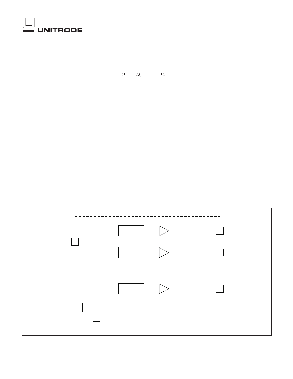
BLOCK DIAGRAM
TRMPWR
2.7V < 5.25V
REF 1.3V
2
REF 1.75V
1.75V +/–50mV
200mA SOURCE/SINK
SOURCE/SINK REGULATOR
REF 0.75V
0.75V +/–50mV
200mA SOURCE/SINK
4
PGND
1.3V +/– 0.1V
7
3
DIFSENS
REG16
REG2
UDG-98093
SLUS413 - MAY 1999
UCC561
ABSOLUTE MAXIMUM RATINGS
TERMPWR . . . . . . . . . . . . . . . . . . . . . . . . . . . . . . . . . . . . . +6V
Package Dissipation . . . . . . . . . . . . . . . . . . . . . . . . . . . . . 1.2W
Junction Temperature. . . . . . . . . . . . . . . . . . . –55°C to +150°C
Storage Temperature . . . . . . . . . . . . . . . . . . . –65°C to +150°C
Currents are positive into, negative out of the specified terminal. Consult Packaging Section of Databook for thermal limitations and considerations of packages.
RECOMMENDED OPERATING CONDITIONS
TERMPWR Voltage . . . . . . . . . . . . . . . . . . . . . . . 2.7V to 5.25V
CONNECTION DIAGRAMS
SOIC-16 (TOP VIEW)
DP Packages
N/C
1
N/C
2
3
4
5
6
7
8
TERMPWR
REG2
HSPGND
HSGND
REG1
DIFSENS
16
15
14
13
12
11
10
9
N/C
N/C
N/C
HSGND
HSGND
N/C
N/C
N/C
ELECTRICAL CHARACTERISTICS:
Unless otherwise specified these specifications apply for TA = 0°C to 70°C,
TERMPWR = 3.3V.
PARAMETER TEST CONDITIONS MIN TYP MAX UNITS
TERMPWR Supply Current Section
TERMPWR Supply Current No Load 40.0 mA
TERMPWR Voltage 2.7 5.25 V
Regulator Section
1.75 Volt Regulator REG1 (± 125mA) 1.7 1.75 1.8 V
1.3 Volt Regulator DIFSENS , No Load 1.2 1.3 1.4 V
0.75 Volt Regulator REG2 (± 125mA) 0.7 0.75 0.8 V
1.75 Volt Regulator Source Current V
= 1.25 –200 mA
O
1.75 Volt Regulator Sink Current VO= 2.25 200 mA
1.75 Volt Sink Current Limit 700 mA
1.75 Volt Source Current Limit –700 mA
1.3 Volt Regulator Source Current DIFSENS, GND –5 –15 mA
1.3 Volt Regulator Sink Current DIFSENS, 2.4V 50 200 µA
0.75 Volt Regulator Source Current VO= 0.25 –200 mA
0.75 Volt Regulator Sink Current VO= 1.25 200 mA
0.75 Source Current Limit 700 mA
0.75 Sink Current Limit –700 mA
Note 1: Guaranted by design. Not 100% tested in production.
2
APPLICATION INFORMATION
TERMPWR
2.7V TO5.25V
2 TERMPWR
4.7µF
DIFSENS: SOURCE ONLY
FROM TERMPWR
4PGND
REF
1.3V
SOURCE/SINK REGULATOR
REF
1.75V
200mA SOURCE/SINK
SOURCE/SINK REGULATOR
REF
0.75V
200mA SOURCE/SINK
1.3V ±0.1V
1.75V ±–50mV
0.75V ±–50mV
7
6
3
DIFSENS
REG1
4.7µF
REG2
UCC561
DIFSENS
475 1%
L1–
121 1%
475 1%
L1+
4.7µF
Figure 1. LVD SCSI discrete resistor stack.
Table I. Resistor stack vs. standard.
Outputs Specification
107.3
112.9mV Diff Bias 100mV to 125mV
237
1.25V Common Mode 1.2V to 1.30V
Application Note: The resistor stack with the 1.75V and 0.75V
reference will give the correct differential impedance, bias voltage, common mode differential impedance and common mode
voltage as show in Table 1.
Diff 100 to 110
Common Mode 100 to 300
475 1%
475 1%
L27–
121 1%
L27+
UDG-98096
UNITRODE CORPORATION
7 CONTINENTALBLVD. • MERRIMACK, NH 03054
TEL. (603) 424-2410 • FAX (603) 424-3460
3

IMPORTANT NOTICE
T exas Instruments and its subsidiaries (TI) reserve the right to make changes to their products or to discontinue
any product or service without notice, and advise customers to obtain the latest version of relevant information
to verify, before placing orders, that information being relied on is current and complete. All products are sold
subject to the terms and conditions of sale supplied at the time of order acknowledgement, including those
pertaining to warranty, patent infringement, and limitation of liability.
TI warrants performance of its semiconductor products to the specifications applicable at the time of sale in
accordance with TI’s standard warranty. Testing and other quality control techniques are utilized to the extent
TI deems necessary to support this warranty . Specific testing of all parameters of each device is not necessarily
performed, except those mandated by government requirements.
CERTAIN APPLICATIONS USING SEMICONDUCTOR PRODUCTS MAY INVOLVE POTENTIAL RISKS OF
DEATH, PERSONAL INJURY, OR SEVERE PROPERTY OR ENVIRONMENTAL DAMAGE (“CRITICAL
APPLICATIONS”). TI SEMICONDUCTOR PRODUCTS ARE NOT DESIGNED, AUTHORIZED, OR
WARRANTED TO BE SUITABLE FOR USE IN LIFE-SUPPORT DEVICES OR SYSTEMS OR OTHER
CRITICAL APPLICA TIONS. INCLUSION OF TI PRODUCTS IN SUCH APPLICATIONS IS UNDERST OOD TO
BE FULLY AT THE CUSTOMER’S RISK.
In order to minimize risks associated with the customer’s applications, adequate design and operating
safeguards must be provided by the customer to minimize inherent or procedural hazards.
TI assumes no liability for applications assistance or customer product design. TI does not warrant or represent
that any license, either express or implied, is granted under any patent right, copyright, mask work right, or other
intellectual property right of TI covering or relating to any combination, machine, or process in which such
semiconductor products or services might be or are used. TI’s publication of information regarding any third
party’s products or services does not constitute TI’s approval, warranty or endorsement thereof.
Copyright 1999, Texas Instruments Incorporated
 Loading...