

The UCC5610 provides 18 line s of active termination for a SCSI (Small
Computer Systems Interface) parallel bus. The SCSI standard recommends active termination at both ends of the cable.
The UCC5610 is ideal for high performance 3.3V SCSI systems. The key
features co ntributing to such low operating voltage are the 0.1V drop out
regulator and the 2.75V reference. The reduced reference voltage was
necessary t o accommodate the lower termin ation current dictated in the
SCSI-3 specification. During disconnect the supply current is typically
only 0.5µA, which makes the IC attractive for battery powered systems.
The UCC5610 is designed with an ultra low channel capacitance of
1.8pF, which elimina tes effects on signal i ntegrity from disconnected terminators at interim points on the bus.
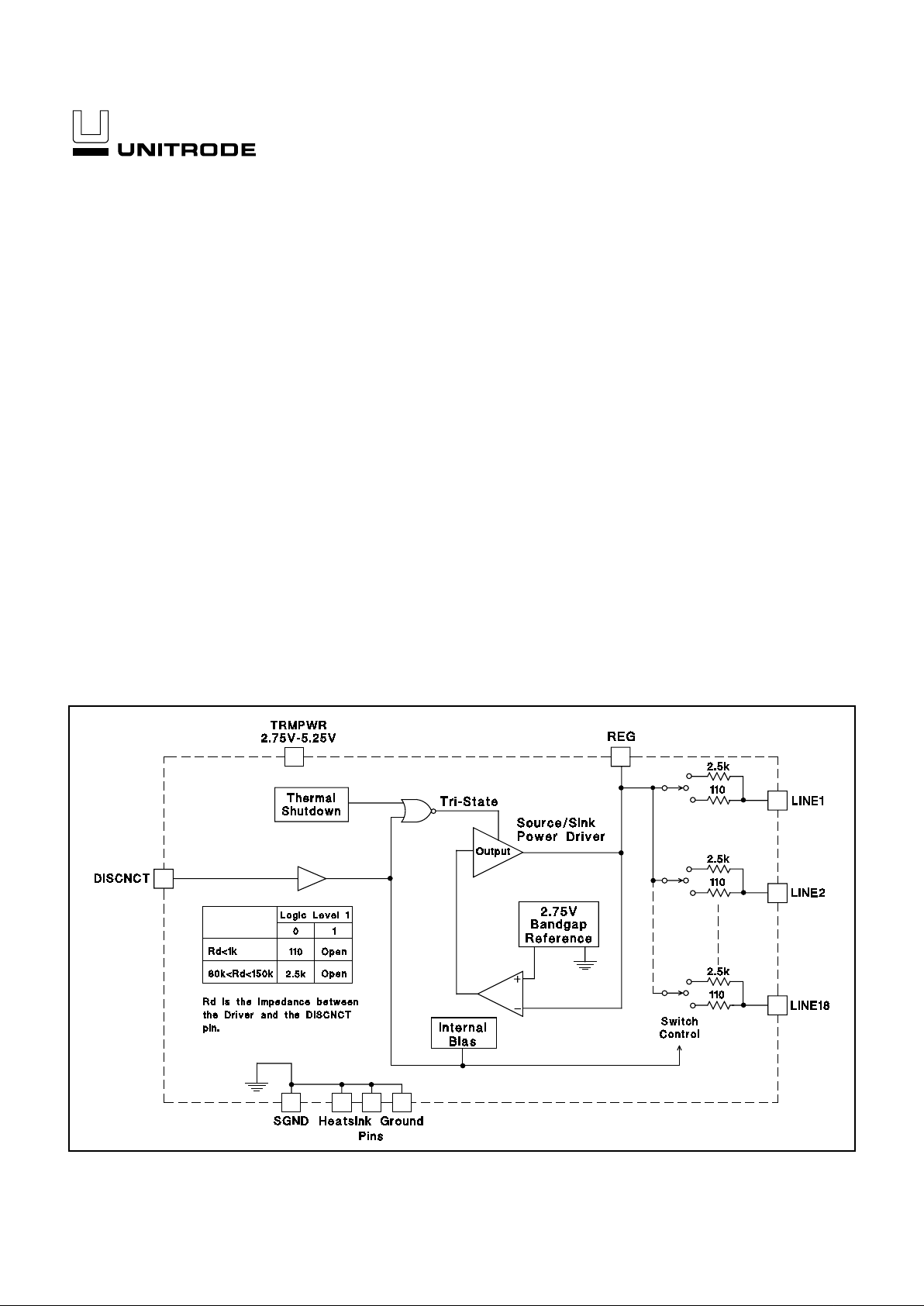
The UCC5610 can be pr ogrammed for either a 110 ohm or 2.5k ohm termination. Th e 110 ohm termination is used for standard SCSI bus lengths
and the 2. 5k ohm term ination is typical ly used in short bus applications.
When driving t he TTL compatible DISCNCT pin directly, the 110 ohm termination is connected when the D ISCNCT pin is driven low, and disconnected whe n driven high. When the DISCNCT pin is driven through an
impedance between 80k and 150k, the 2.5k ohm termination is connected when the DISCNCT pin is driven low, and disconnected when
driven high.
UCC5610
18-Line 3-5 Volt Low Capacitance SCSI Active Terminator
FEATURES DESCRIPTION
BLOCK DIAGRAM
Circuit Design Patented
•
Complies with SCSI, SCSI-2, SCSI-3
and FAST-20 (Ultra) Standards
•
2.75V to 7V Operation
•
1.8pF Channel Capacitance during
Disconnect
•
0.5µA Supply Current in Disconnect
Mode
•
110 Ohm/2.5k Programmable
Termination
•
Completely Meets SCSI Hot Plugging
•
-650mA Sourcing Current for
Termination
•
+400mA Sinking Current for Active
Negation Drivers
•
Trimmed Termination Current to 4%
•
Trimmed Impedance to 7%
•
Current Limit and Thermal Shutdown
Protection
continued
2/97
UDG-94128-1
UCC5610
The power amplifier output stage allows the UCC5610 to
source full termination current and sink active negation
current when all termination lines are actively negated.
The UCC5610 is pin for pin compatible with Unitrode’s
other 18 line SCSI terminators, allowing lower capacitance and lower voltage upgrades to existing systems.
The UCC5610, a s with all Unitrode terminators, is completely hot pluggable and appears as high impedanc e at
the terminating channels with V
TRMPWR
= 0V or open.
Internal circuit trimming is utilized, first to trim the 110
ohm terminati on impedan ce to a 7% tolera nce, and then
most importantly, to trim the output current to a 4% tolerance, as close to the max SCSI-3 spec as possible,
which maxi mizes noise margin in FAST-20 SCSI operation.
Other features include thermal shutdown and current
limit.
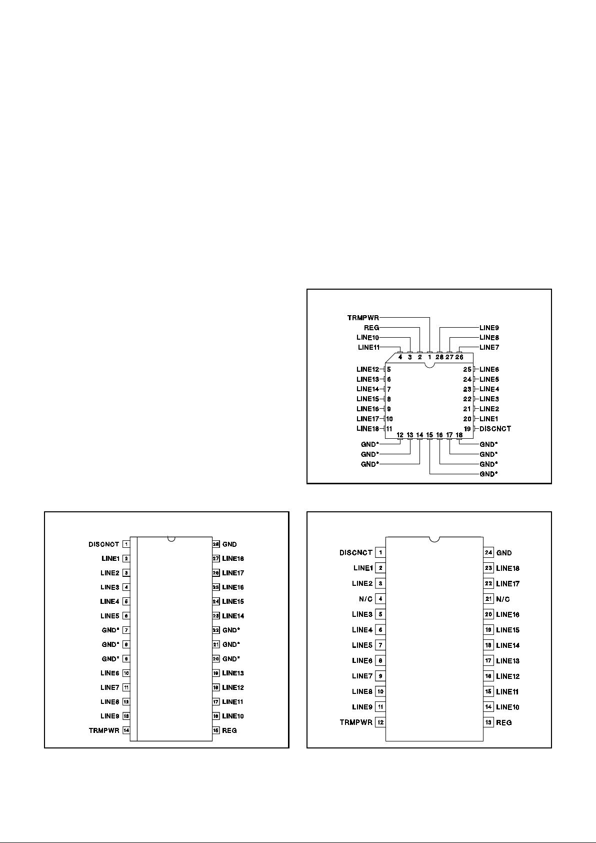
This device i s offered in low thermal resistance versions
of the ind ustry standard 28 pin wide body SOIC, 24 pin
wide body DIP and 28 pin PLCC.
ABSOLUTE MAXIMUM RATINGS
Termpwr Vo ltage . . . . . . . . . . . . . . . . . . . . . . . . . . . . . . . . . +7V
Signal Line Voltage. . . . . . . . . . . . . . . . . . . . . . . . . . . 0V to +7V
Regulator Output Current . . . . . . . . . . . . . . . . . . Self-regulating
Storage Temperature . . . . . . . . . . . . . . . . . . . −65°C to +150°C
Operating Temperature . . . . . . . . . . . . . . . . . −55°C to +150°C
Lead Temperature (Soldering, 10 Sec.). . . . . . . . . . . . . +300°C
RECOMMENDED OPERATING CONDITIONS
Termpwr Voltage . . . . . . . . . . . . . . . . . . . . . . . . 2.75V to 5.25V
Signal Line Voltage. . . . . . . . . . . . . . . . . . . . . . . . . . . 0V to +5V
Disconnect Input Voltage . . . . . . . . . . . . . . . . . . 0V to Termpwr
Description Continued
Unless otherwise sp ec ified all voltages are with respect to
Ground. Currents are positive into, negative out of the specified terminal.
Consult Packaging Section of Unitrode Integrated Circuits databook for thermal limitations and considerations of packages.
CONNECTION DIAGRAMS
PLCC-28 (Top View)
QP Package
* QP package pins 12 - 18 serve as both heatsink and signal
ground.
* DWP package pin 28 serves as signal ground; pins 7, 8, 9,
20, 21, 22 serve as heatsink/ground.
SOIC-28 (Top View)
DWP Package
Note: Drawings are not to scale.
DIL-24 (Top View)
N or J Package
2

UCC5610
PARAMETER TEST CONDITIONS MIN TYP MAX UNITS
Supply Current Section
Termpwr Supply Current All termination lines = Open 1 2 mA
All termination lines = 0.2V 415 455 mA
Power Down Mode DISCNCT = Termpwr 0.5 5
µ
A
Output Section (110 ohms - Terminator Lines)
Terminator Impedance (Note 4) 102.3 110 117.7 Ohms
Output High Voltage (Note 1) 2.5 2.7 3.0 V
Max Output Cur r e nt V
LINE
= 0.2V, TJ = 25°C
−
22.1−23
−
24 mA
V
LINE
= 0.2V −21 −23 −24 mA
V
LINE
= 0.2V, TRMPWR = 3V, TJ = 25°C (Note 1) −20.2 −23 −24 mA
V
LINE
= 0.2V, TRMPWR = 3V (Note 1) −19 −23 −24 mA
V
LINE
= 0.5V
−
22.4 mA
Output Leakage DISCNCT = 2.4V, TRMPWR = 0V to 5.25V 10 400 nA
Output Capacitance DISCNCT = 2.4V (Note 2, 3) (DWP Package) 1.8 2.5 pF
Output Section (2.5k ohms - Terminator Lines) (R
DISCNCT
= 80k ohms)
Terminator Impedance 22.53kΩ
Output High Voltage TRMPWR = 3V (Note 1) 2.5 2.7 3.0 V
Max Output Cur r e nt V
LINE
= 0.2V −0.7 −1 −1.4 mA
V
LINE
= 0.2V, TRMPWR = 3V (Note 1) −0.6 −1 −1.5 mA
Output Leakage DISCNCT = 2.4V, TRMPWR = 0 to 5.25V 10 400 nA
Output Capacitance DISCNCT = 2.4V (Note 2, 3) (DWP Package) 1.8 2.5 pF
Regulator Section
Regulator Output Voltage 5.25V > TRMPWR > 3V 2.5 2.7 3.0 V
Drop Out Voltage All Termination Lines = 0.2V 0.1 0.2 V
Short Circuit Current V
REG
= 0V −450 −650 −800 mA
Sinking Current Capability V
REG
= 3V 200 400 800 mA
Thermal Shutdown (Note 2) 170 °C
Thermal Shutdown Hysteresis (Note 2) 10 °C
Disconnect Section
Disconnect Threshold R
DISCNCT
= 0 & 80k 0.8 1.5 2.0 V
Input Current DISCNCT = 0V 30 50 µA
ELECTRICAL CHARACTERISTICS
Unless otherwise st at ed, th ese sp ecif icat io ns app ly for TA = 0°C to 70°C.
TRMPWR = 3.3V, DISCNCT = 0V, R
DISCNCT
= 0 ohms. TA = TJ.
Note 1: Measuring each termin ation line while other 17 are low (0.2V).
Note 2: Guaranteed by desig n. Not 100% tested in production.
Note 3: Output capacitance is measured at 0.5V.
Note 4: Tested by measuring I
OUT
with V
OUT
= 0.2V and V
OUT
= V
REG
- 0.1V then calculating the impedance.
3

UCC5610
Figure 1: Typical SCSI Bus Configurations Utilizing A UCC5610 Device
APPLICATION INFORMATION
UDG-94130
UNITRODE CORPORATI ON
7 CONTINENTAL BLVD. • MERRIMACK, NH 03054
TEL. (603) 424- 24 10 • FAX (603) 424-3460
4

IMPORTANT NOTICE
T exas Instruments and its subsidiaries (TI) reserve the right to make changes to their products or to discontinue
any product or service without notice, and advise customers to obtain the latest version of relevant information
to verify, before placing orders, that information being relied on is current and complete. All products are sold
subject to the terms and conditions of sale supplied at the time of order acknowledgement, including those
pertaining to warranty, patent infringement, and limitation of liability.
TI warrants performance of its semiconductor products to the specifications applicable at the time of sale in
accordance with TI’s standard warranty. Testing and other quality control techniques are utilized to the extent
TI deems necessary to support this warranty. Specific testing of all parameters of each device is not necessarily
performed, except those mandated by government requirements.
CERT AIN APPLICATIONS USING SEMICONDUCTOR PRODUCTS MA Y INVOLVE POTENTIAL RISKS OF
DEATH, PERSONAL INJURY, OR SEVERE PROPERTY OR ENVIRONMENTAL DAMAGE (“CRITICAL
APPLICATIONS”). TI SEMICONDUCTOR PRODUCTS ARE NOT DESIGNED, AUTHORIZED, OR
WARRANTED TO BE SUITABLE FOR USE IN LIFE-SUPPORT DEVICES OR SYSTEMS OR OTHER
CRITICAL APPLICATIONS. INCLUSION OF TI PRODUCTS IN SUCH APPLICA TIONS IS UNDERSTOOD T O
BE FULLY AT THE CUSTOMER’S RISK.
In order to minimize risks associated with the customer’s applications, adequate design and operating
safeguards must be provided by the customer to minimize inherent or procedural hazards.
TI assumes no liability for applications assistance or customer product design. TI does not warrant or represent
that any license, either express or implied, is granted under any patent right, copyright, mask work right, or other
intellectual property right of TI covering or relating to any combination, machine, or process in which such
semiconductor products or services might be or are used. TI’s publication of information regarding any third
party’s products or services does not constitute TI’s approval, warranty or endorsement thereof.
Copyright 1999, Texas Instruments Incorporated
 Loading...