

Datasheet UCC5606PWPTR, UCC5606PWP, UCC5606N, UCC5606J, UCC5606DPTR Datasheet (Texas Instruments)
...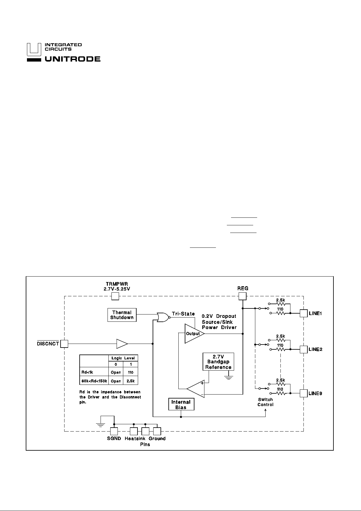
The UCC5606 provides 9 lines of active termination for a SCSI (Small
Computer Systems Interface) parallel bus. The SCSI standard recommends active termination at both ends of the cable segment.
The UCC5606 is ideal for high performance 3.3V SCSI systems. The key
features contributing to such low operating voltage are the 0.1V drop out
regulator and the 2.7V reference. The reduced reference voltage was
necessary to accommodate the lower termi nation current dictated in the
SCSI-3 specification. During disconnect the supply current is typically
only 1µA, which makes the IC attractive for batt ery powered syst ems.
The UCC5606 is designed with an ultra low channel capacitance of
1.8pF, which eliminates effects on signal integri ty from disconnected terminators at interim points on the bus.
The UCC5606 can be programmed for either a 110 ohm or 2.5k ohm termination. The 110 ohm termination is used for standard SCSI bus lengths
and the 2.5k ohm terminati on is typically used in short bus applications.
When driving the TTL compatible
DISCNCT pin directly, the 110 ohm ter-
mination is connected when the
DISCNCT pin is driven high, and discon-
nected when low. When the
DISCNCT pin is driven through an
impedance between 80k and 150k, the 2.5k ohm termination is connected when the
DISCNCT pin is driven h igh, and disconnected when
driven low.
UCC5606
9-Line 3-5 Volt SCSI Active Terminator, Reverse Disconnect
FEATURES DESCRIPTION
BLOCK DIAGRAM
Circuit Design Patented
• Complies with SCSI, SCSI-2 and
SCSI-3 Standards
• 2.7V to 7V Operation
• 1.8pF Channel Capacitance during
Disconnect
• 1µA Supply Current in Disconnect
Mode
• 110 Ohm/2.5k Programmable
Termination
• Completely Meets SCSI Hot Plugging
• -400mA Sourcing Current for
Termination
• +400mA Sinking Current for Active
Negation Drivers
• Trimmed Termination Current to 4 %
• Trimmed Impedance to 7%
• Current Limit and Thermal Shutdown
Protectio n
continue d
5/95
UDG-94067-1
UCC5606
The power amplifier output stage allows the UCC5606 to
source full termination current and sink active negation
current when all termination lines are actively negated.
The UCC5606 is pin for pin compatible with Unitrode’s
other 9 line SCSI terminators, except that
DISCNCT is
now active low, allowing lower capacitance and lower
voltage upgrades to existing systems. The UCC5606, as
with all Uni trode terminators, is completely hot pluggable
and appears as high imped ance at the terminating channels with V
TRMPWR = 0V or open.
Internal circuit trimming is utilized, first to trim the 110
ohm termination impeda nce to a 7% tole rance, and then
most importantly, to trim the output current to a 4% tolerance, as close to the max SCSI-3 spec as possible,
which maximizes noise margin in fast SCSI operation.
Other features include thermal shutdown and current
limit.
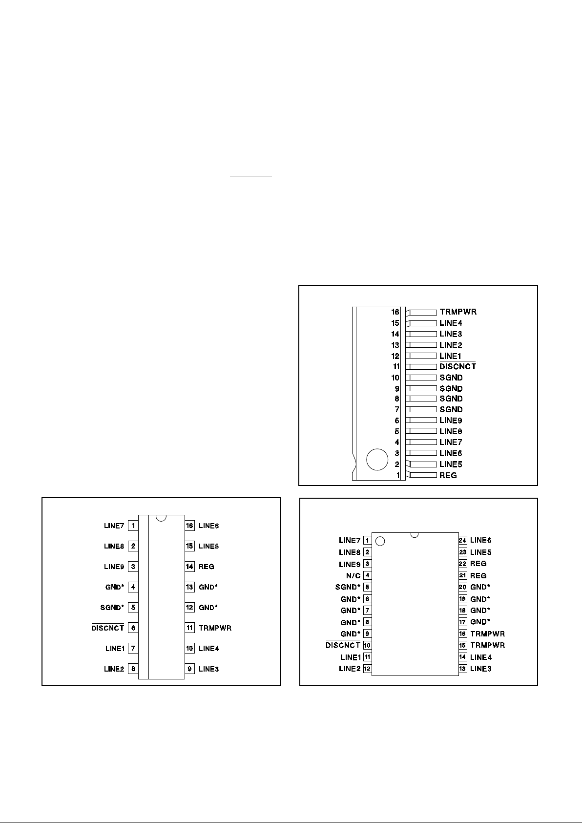
This device is offered in low thermal resistance versions
of the industry standard 16 pin narrow body SOIC, 16 pin
ZIP (Zig-Zag In Line package), 24 pin TSSOP and 28 pin
PLCC.
ABSOLUTE MAXIMUM RATINGS
Termpwr Voltage . . . . . . . . . . . . . . . . . . . . . . . . . . . . . . . . . +7V
Signal Line Voltage. . . . . . . . . . . . . . . . . . . . . . . . . . . 0V to +7V
Regulator Output Curren t. . . . . . . . . . . . . . . . . . . . . . . . . . 0.6A
Storage Temperature . . . . . . . . . . . . . . . . . . . −−65°C to +150°C
Operating Tem pe ratur e . . . . . . . . . . . . . . . . . −−55°C to +150°C
Lead Temperat ure (Solde ring, 10 Sec .). . . . . . . . . . . . . +300°C
RECOMMENDED OPERATING CONDITIONS
Termpwr Voltage . . . . . . . . . . . . . . . . . . . . . . . . . 2 .7 V to 5.25 V
Signal Line Voltage. . . . . . . . . . . . . . . . . . . . . . . . . . . 0V to +5V
Disconnect Input Voltage . . . . . . . . . . . . . . . . . . 0V to Termpwr
Description Continued
Unless otherwise specified all volta ges ar e with respect to
Ground. Cur rents are positive into, negative out of the specified terminal.
Consult Packaging Sectio n of Unitr ode Int egr at ed Circ uits databook for thermal limitations and con sider at ions of pack ages .
CONNECTION DIAG RAMS
SOIC-16 (Top View)
DP Package
TSSOP-24 (Top View)
PWP Package
* DP package pin 5 ser ves as signal ground; pins 4, 12, 13
serve as heatsink/ground.
* PWP packa ge pin 5 serves as signal ground ; pins 6, 7, 8, 9,
17, 18, 19, and 20 ser ve as heat sink/ gr oun d.
ZIP-16 (Top View)
Z Package
Note: Drawings are not to scale.
2

UCC5606
Note: Drawings are not to scale.
DIL-16 (Top View)
N or J Package
CONNECTION DIAG RAMS (cont.)
PARAMETER TEST CONDITIONS MIN TYP MAX UNITS
Supply Cur ren t Sectio n
Termpwr Supply Cur rent All termination lines = Open 1 2 mA
All termination lines = 0.2V 210 218 mA
Power Down Mode
DISCNCT = 0V 0.5 5 µA
Output Secti on (1 10 ohm s - Term i nat or Lines)
Terminator Impedance 102.3 110 117.7 Ohms
Output High Voltag e TRMPWR = 3V (Note 1) 2.5 2.7 3.0 V
Max Output Current V
LINE = 0.2V, TJ = 25°C −−22.1 −−23 −−24 mA
V
LINE = 0.2V −−21 −−23 −−24 mA
V
LINE = 0.2V, TRMPWR = 3V, TJ = 2 5° C (No te 1) −−20.2 −−23 −−24 mA
V
LINE = 0.2V, TRMPWR = 3V (Note 1) −−19 −−23 −−24 mA
V
LINE = 0.5V −−22.4 mA
Output Leakage
DISCNCT = 0V, TRMPWR = 0V to 5.25V 10 400 nA
Output Capacitance
DISCNCT = 0V, DP Package (Note 2) 1.8 2.5 pF
Output Secti on (2 .5 k ohms - Term i nat or Line s) (RDISCNCT = 80k ohms)
Terminator Impedance 22.53kΩ
Output High Voltag e TRMPWR = 3V (Note 1) 2.5 2.7 3.0 V
Max Output Current V
LINE = 0.2V −−0.7 −−1 −−1.4 mA
V
LINE = 0.2V, TRMPWR = 3V (Note 1) −−0.6 −−1 −−1.5 mA
Output Leakage
DISCNCT = 0V, TRMPWR = 0 to 5.25V 10 400 nA
Output Capacitance
DISCNCT = 0V, DP Package (Note 2) 1.8 2.5 pF
Regul ator Secti o n
Regulator Output Voltag e 5.25V > TRMPWR > 3V 2.5 2.7 3.0 V
Drop Out Voltage All Termin atio n Lines = 0.2 V 0.1 0.2 V
ELECTRICAL CHARACTERISTICS Unless otherwise stated, these specifications apply for TA = 0°C to 70°C.
TRMPWR = 3.3V,
DISCNCT = 3.3V, RDISCNCT = 0 ohms. TA = TJ .
3

UCC5606
Note 1: Measuring each terminat ion l ine while other 8 are low (0.2V).
Note 2: Guaranteed by design. Not 100% tested in product ion.
PARAMETER TEST CONDITIONS MIN TYP MAX UNITS
Regulat or Sec tion ( cont .)
Short Circuit Cur rent V
REG = 0V −−200 −−400 −−800 mA
Sinking Current Capa b ility VREG = 3V 200 400 800 mA
Thermal Shutdo wn (Note 2) 170 °C
Thermal Shu td own Hyst er esis (Note 2) 10 °C
Disconnect Section
Disconnect Threshold R
DISCNCT = 0 & 80k 0.8 1.5 2.0 V
Input Current
DISCNCT = 3.3V 30 50 µA
ELECTRICAL CHARACTERISTICS (cont.) Unless otherwise stated, these specifications apply for TA=0°C to 70°C.
TRMPWR = 3.3V,
DISCNCT = 3.3V, RDISCNCT = 0 ohms. TA = TJ .
Figure 1: Typical SCSI Bus Configurations Utilizing 2 UCC5606 Devices
Figure 2: Typical Wide SCSI Bus Configura ti ons Utilizing 3 UCC5606 Dev ic es.
APPLICATION INFORMATION
UDG-94068
UDG-94069
UNITRODE INTEGRATED CIRCUITS
7 CONTINENTAL BLVD. • MERRIMACK, NH 03054
TEL. (603) 424-2410 • FAX (603) 424-3460
4

IMPORTANT NOTICE
T exas Instruments and its subsidiaries (TI) reserve the right to make changes to their products or to discontinue
any product or service without notice, and advise customers to obtain the latest version of relevant information
to verify, before placing orders, that information being relied on is current and complete. All products are sold
subject to the terms and conditions of sale supplied at the time of order acknowledgement, including those
pertaining to warranty, patent infringement, and limitation of liability.
TI warrants performance of its semiconductor products to the specifications applicable at the time of sale in
accordance with TI’s standard warranty. Testing and other quality control techniques are utilized to the extent
TI deems necessary to support this warranty. Specific testing of all parameters of each device is not necessarily
performed, except those mandated by government requirements.
CERT AIN APPLICATIONS USING SEMICONDUCTOR PRODUCTS MAY INVOLVE POTENTIAL RISKS OF
DEATH, PERSONAL INJURY, OR SEVERE PROPERTY OR ENVIRONMENTAL DAMAGE (“CRITICAL
APPLICATIONS”). TI SEMICONDUCTOR PRODUCTS ARE NOT DESIGNED, AUTHORIZED, OR
WARRANTED TO BE SUITABLE FOR USE IN LIFE-SUPPORT DEVICES OR SYSTEMS OR OTHER
CRITICAL APPLICATIONS. INCLUSION OF TI PRODUCTS IN SUCH APPLICA TIONS IS UNDERSTOOD T O
BE FULLY AT THE CUSTOMER’S RISK.
In order to minimize risks associated with the customer’s applications, adequate design and operating
safeguards must be provided by the customer to minimize inherent or procedural hazards.
TI assumes no liability for applications assistance or customer product design. TI does not warrant or represent
that any license, either express or implied, is granted under any patent right, copyright, mask work right, or other
intellectual property right of TI covering or relating to any combination, machine, or process in which such
semiconductor products or services might be or are used. TI’s publication of information regarding any third
party’s products or services does not constitute TI’s approval, warranty or endorsement thereof.
Copyright 1999, Texas Instruments Incorporated
 Loading...