

UCC5510
SLUS332A - OCTOBER 1999
FEATURES
•
Auto Selection Multi-Mode Single
Ended or Low Voltage Differential
Termination
•
3.0V to 5.25V Operation
•
Differential Failsafe Bias
•
Thermal Packaging for Low Junction
Temperature and Better MTBF
•
Master/Slave Inputs
•
Supports Active Negation
•
3pF Channel Capacitance
Low Voltage Differential (LVD/SE) SCSI 9 Line Terminator
1
REG
DIFFSENS
5L1–
4L1+
32 L9–
31 L9+
125
+50mV TO +62.5mV
SWITCHES UP ARE SINGLE
ENDED SWITCHES DOWN ARE
LOW VOLTAGE DIFFERENTIAL
0.7 > 0.6V
2.2 > 1.9V
SE GND
SWITCH
52
110
52
125
+50mV TO +62.5mV
52
110
52
DEVICE MODE
SELECT LOG IC
21DIFFB
REF 2.7V
REF 1.25V
19MSTR/SLV
38TRMPWR +VDD
REF 1.3V
1.3V ± –0.1V
20
SOURCE 5 < 15mA
SINK 200µA MAXIMUM (NOISE LOAD)
8HS/GND
28
27
26
10
9
18
HS/GND
HS/GND
HS/GND
HS/GND
HS/GND
GND
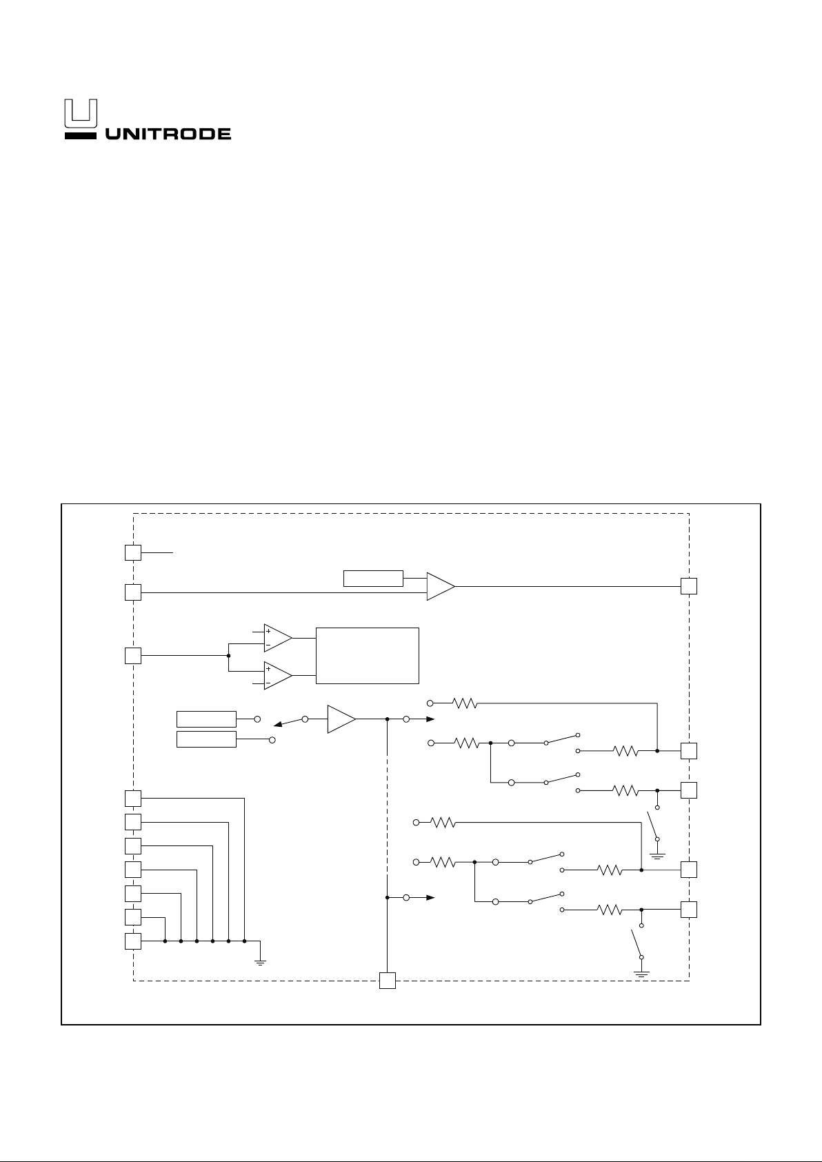
BLOCK DIAGRAM
UDG-98033
DESCRIPTION
The UCC5510 Multi-Mode Low Voltage Differential and Single Ended
Terminator is specially designed for automatic termination of SingleEnded or Low Voltage Differential SCSI Bus.The Multi-Mode operation of
this device allows for a transition system design for the next generation
SCSI Parallel Interface (SPI-2). Compliant with SPI-2, with SPI and Fast20 the UCC5510 incorporates all the functions necessary to properly ter
-
minate the SCSI Bus and has internal thermal shut down and short cir
-
cuit limiting.
Circuit Design Patented
2
UC5510
L3+
HS/GND
L9–
L9+
L8–
TRMPWR
N/C
N/C
HS/GND
L2–
HS/GND
L1+
L1–
L2+
REG
HS/GND
L3–
L8+
HS/GND
HS/GND
L4+
L4–
14
13
12
11
10
9
8
7
6
5
4
3
2
1
23
24
25
26
27
28
29
30
31
32
33
34
35
36
18
17
16
15
DIFF B
MSTR/SLV
DIFFSENS
19
20
21
22L5+
L5–
N/C
GND
L7–
L7+
L6–
L6+
N/C
N/C
N/C
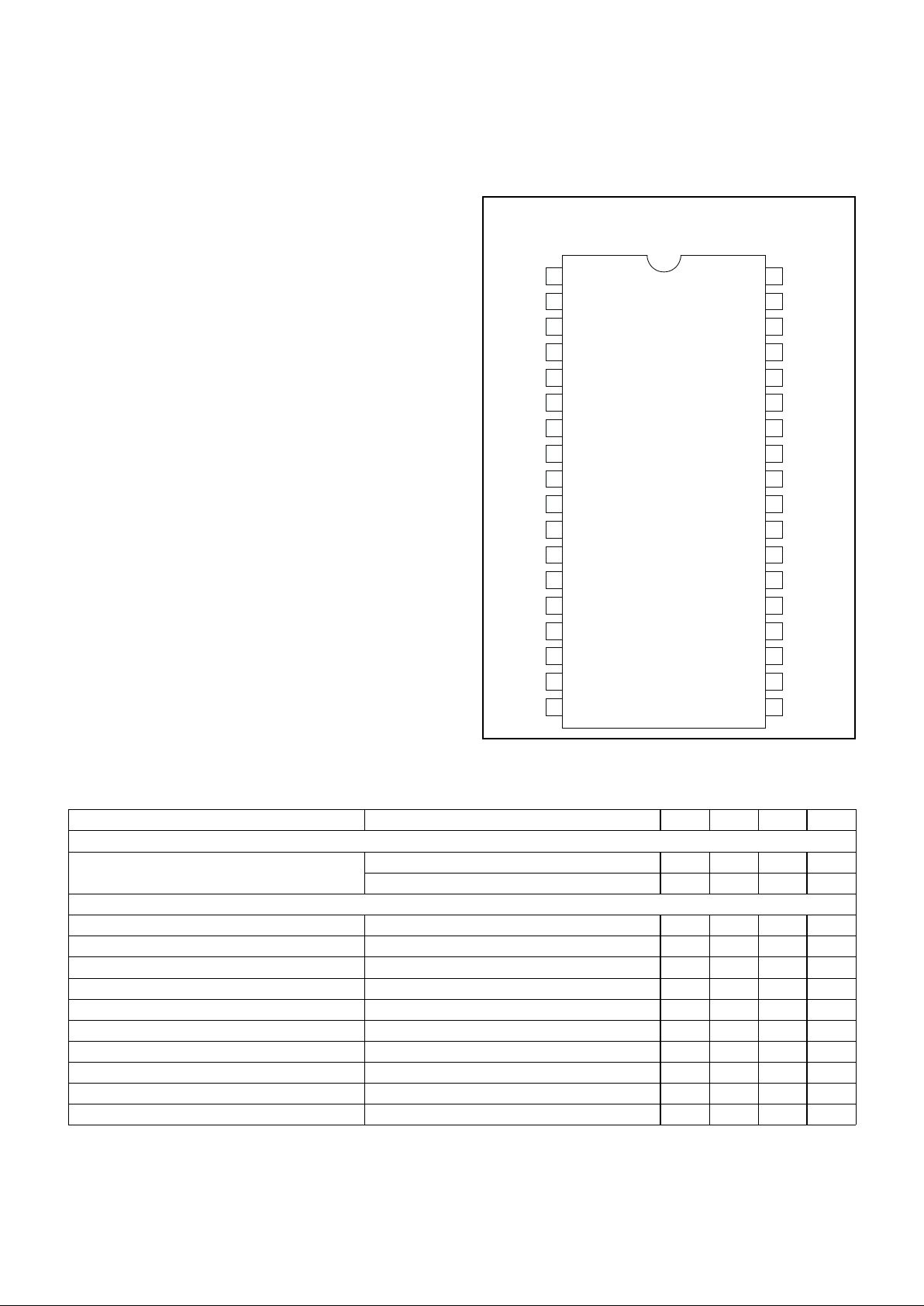
CONNECTION DIAGRAM
SSOP-36 (Top View)
MWP Package
ELECTRICAL CHARACTERISTICS: Unless otherwise specified, TA = 0°C to 70°C, TRMPWR = 3.3V.
PARAMETER TEST CONDITIONS MIN TYP MAX UNITS
TRMPWR Supply Current Section
TRMPWR Supply Current 20 mA
Disable Terminator, in DISCNCT mode. 35 µA
Regulator Section
1.25V Regulator LVD Mode 1.15 1.25 1.35 V
1.25V Regulator Source Current LVD Mode, Differential Sense Floating –80 –100 mA
1.25V Regulator Sink Current LVD Mode, Differential Sense Floating 80 100 mA
1.3V Regulator DIFFSENS 1.2 1.3 1.4 V
1.3V Regulator Source Current DIFFSENS –5 –15 mA
1.3V Regulator Sink Current DIFFSENS 50 200 µA
2.7V Regulator Single Ended Mode 2.5 2.7 3 V
2.7V Regulator Source Current Single Ended Mode –200 –400 –800 mA
2.7V Regulator Sink Current Single Ended Mode 100 200 400 mA
2.7V Regulator Dropout Voltage V
TRMPWR
– (V
REG
– 3.0 Min) 200 mV
ABSOLUTE MAXIMUM RATINGS
TRMPWR Voltage. . . . . . . . . . . . . . . . . . . . . . . . . . . . . . . . . 6V
Signal Line Voltage . . . . . . . . . . . . . . . . . . . . . 0V to TRMPWR
Package Power Dissipation . . . . . . . . . . . . . . . . . . . . . . . . . 2W
Storage Temperature . . . . . . . . . . . . . . . . . . . –65°C to +150°C
Junction Temperature. . . . . . . . . . . . . . . . . . . –55°C to +150°C
Lead Temperature (Soldering, 10sec.) . . . . . . . . . . . . . +300°C
RECOMMENDED OPERATING CONDITIONS
TRMPWR Voltage . . . . . . . . . . . . . . . . . . . . . . . 3.0V TO 5.25V
All voltages are with respect to pin 1.Currents are positive into,
negative out of the specified terminal. Consult Packaging Sec
tion of the Databook for thermal limitations and considerations of
packages.

3
UC5510
ELECTRICAL CHARACTERISTICS: Unless otherwise specified, TA = 0°C to 70°C, TRMPWR = 3.3V.
PARAMETER TEST CONDITIONS MIN TYP MAX UNITS
Differential Termination Section
Differential Impedance 100 105 110 Ω
Common Mode Impedance 110 125 165 Ω
Differential Bias Voltage Drivers Tri-stated 100 125 mV
Common Mode Bias 1.25 V
Output Capacitance Single Ended Measurement to Ground (Note 1) 3 pF
Single Ended Termination Section
Impedance 102.3 110 117.7 Ω
Termination Current Signal Level 0.2V –21 –23 –24 mA
Signal Level 0.5V –22.4 mA
Output Leakage Disabled, TRMPWR = 0V to 5.25V 400 nA
Output Capacitance Single Ended Measurement to Ground (Note 1) 3 pF
Single Ended GND SW Impedance 60 Ω
Differential Sense (DIFF B) Input Sections
DIFFB Single Ended Threshold 0.6 0.7 V
DIFFB Sense LVD Threshold 1.9 2.2 V
DIFFB Input Current V
DIFFB
= 0V and 3.3V –10 10 µA
Master/Slave (MSTR/SLV) Input Section
MSTR/SLV Threshold 0.8 2 V
MSTR/SLV Input Current –30 30 µA
Note 1: Guaranteed by design. Not 100% tested in production.
PIN DESCRIPTIONS
DIFFB: DIFF SENSE filter pin should be connected to a
0.1µF capacitor to GND and 20k resistor to SCSI/Bus
DIFF SENSE Line.
DIFFSENS: The SCSI bus DIFF SENSE line is driven to
1.3V to detect what type of devices are connected to the
SCSI bus.
HS/GND: Heat Sink GND. Connect to large area PC
board traces to increase power dissipation capability.
GND: Power Supply Return.
L1– thru L9–: Signal line/active line for single ended or
negative line in differential applications for the SCSI bus.
L1+ thru L9+: Ground line for single ended or positive
line for differential applications for the SCSI bus.
MSTR/SLV: Mode select for the non-controlling termina
-
tor. MSTR enables the 1.3V regulator, when the termina
-
tor is enabled.
Note: This function will be removed on
further generations of the multimode terminators.
REG: Regulator bypass, must be connected to a 4.7µF
capacitor.
TRMPWR: V
IN
3.0V to 5.25V supply.

4
UC5510
UNITRODE CORPORATION
7 CONTINENTAL BLVD. • MERRIMACK, NH 03054
TEL. (603) 424-2410 • FAX (603) 424-3460
TRMPWR
MSTR/SLV
0.1µF
36
19
L1+
DIFFSENS 20
DIFFB
21
TRMPWR
MSTR/SLV
36
19
L1+
DIFFSENS20
DIFFB
21
20k
0.1µF
20k
NO CONNECT
NO CONNECT
TRMPWR
MSTR/SLV
36
19
DIFFSENS
20
DIFFB
21
TRMPWR
MSTR/SLV
36
19
DIFFSENS
20
DIFFB
21
TRMPWR
MSTR/SLV
36
19
DIFFSENS
20
DIFFB
21
TRMPWR
MSTR/SLV
36
19
DIFFSENS
20
DIFFB
21
TRMPWR TRMPWR
CONTROL LINES (9)
L1– L1–
L9+
L9–
L9+
L9–
L10+ L10+
DATA LINES + PARITY
L10– L10–
L18+
L18–
L18+
L18–
L19+ L19+
L19– L19–
L27+
L27–
L27+
L27–
DATA LINES + PARITY
4.7µF
1REG
4.7µF
1REG
4.7µF
1REG
4.7µF
1REG
4.7µF
4.7µF
1REG
4.7µF
1REG
4.7µF
Figure 1. Application Drawing
APPLICATION INFORMATION
UDG-98034a
The master is selected by placing TRMPWR on
MSTR/SLV and enabling the 1.3V regulator. The master
is the only terminator connected directly to the DIFF
SENS bus line. All the other terminators receive a mode
signal by connecting the DIFFB pins together.
The balancing capacitor is very important during high
speed operation. The typical capacitor balance between
the positive (+) and negative (–) signals is 0.1pF, except
in the MWP package where between L8 and L9 the bal
ance is 0.23pF and 0.4pF respecitvely The negative (–)
signal line has a higher capacitance than the positive (+)
signal line. The FQP package has typically 0.2pF less
capacitance than the MWP package, where the typical
balance is 0.1pF except for L8 and L3, where the bal
ance is 0.4pF.
Note: The master/slave function will not be included in future
Unitrode terminators.
 Loading...