

Datasheet UCC3958PWPTR-4, UCC3958PWPTR-3, UCC3958PWPTR-2, UCC3958PWPTR-1, UCC3958PWP-4 Datasheet (Texas Instruments)
...
FEATURES
• Protects Sensitive Lithium-Ion Cells Form
Over Charging and Over Discharging
• Dedicated for One Cell Applications
• Does Not Require External FETs or Sense
Resistors
• Internal Precision Trimmed Charge and
Discharge Voltage Limits
• Extremely Low Power Drain
• Low FET Switch Voltage Drop of 150mV
Typical for 3A Currents
• Short Circuit Current Protection (with User
Programmable Delay)
• 3A Current Capacity
• Thermal Shutdown
• User Controlled Enable Pin
Single Cell Lithium-Ion Battery Protection Circuit
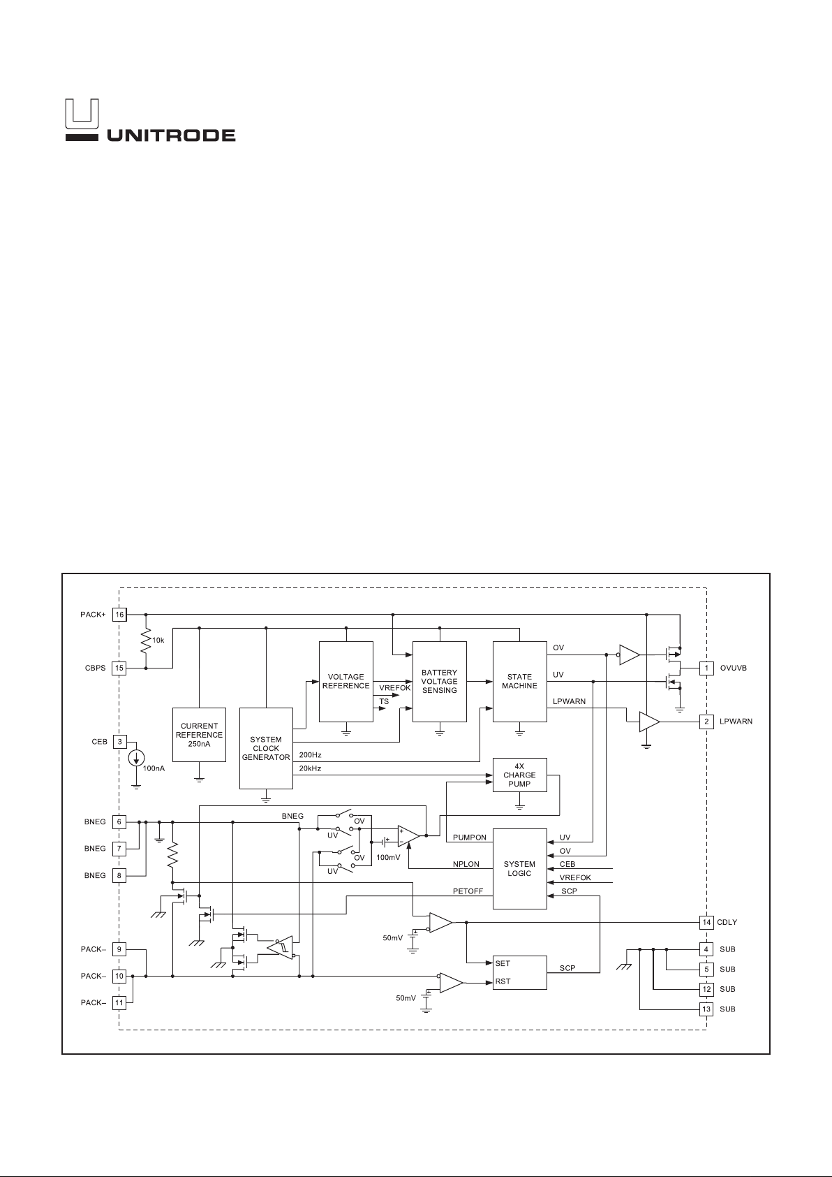
BLOCK DIAGRAM
UDG-98050
UCC3958 -1/-2/-3/-4
PRELIMINARY
DESCRIPTION
UCC3958 is a monolithic BCMOS lithium-ion battery protection
circuit that is designed to enhance the useful operating life of
one cell rechargeable battery packs. Cell protection features
consist of internally trimmed charge and discharge voltage limits, discharge current limit with a delayed shutdown and an ultra
low current sleep mode state when the cell is discharged. Additional features include an on chip MOSFET for reduced external component count and a charge pump for reduced power
losses while charging or discharging a low cell voltage battery
pack. This protection circuit requires a minimum number of external components and is able to operate and safely shutdown
in the presence of a short circuit load.
6/98
2
UCC3958 -1/-2/-3/-4
ELECTRICAL CHARACTERISTICS:
Unless otherwise specified, PACK+ = 4V, –20°C < TA< 70°C. All voltages
measured with respect to BNEG. TA=T
J
.
PARAMETER TEST CONDITIONS MIN TYP MAX UNITS
State Transition Thresholds
NORM to OV (VOV) UCC3958-1 4.15 4.20 4.25 V
OV to NORM (V
THI
) UCC3958-1 3.85 3.90 3.95 V
NORM to OV (VOV) UCC3958-2 4.20 4.25 4.30 V
OV to NORM (V
THI
) UCC3958-2 3.90 3.95 4.00 V
NORM to OV (VOV) UCC3958-3 4.25 4.30 4.35 V
OV to NORM (V
THI
) UCC3958-3 3.95 4.00 4.05 V
NORM to OV (V
OV
) UCC3958-4 4.30 4.35 4.40 V
OV to NORM (V
THI
) UCC3958-4 4.00 4.05 4.10 V
NORM to UV (VUV) (Note 1) 2.25 2.35 2.45 V
UV to NORM (V
TLO
) 2.55 2.65 2.75 V
OV, UV Delay Time (TD) All Dash Numbers 7 18 34 msec
ABSOLUTE MAXIMUM RATINGS
Supply Voltage (PACK+ to BNEG)...................7.5V
Maximum Continuous Charge Current .................3A
Maximum Charger Voltage (PACK+ to PACK–) ..........9V
Maximum Reverse Voltage (PACK+ to PACK–) .........–8V
Storage Temperature ...................–65°C to +150°C
Junction Temperature...................–55°C to +150°C
Lead Temperature (Soldering, 10 sec.) .............+300°C
Currents are positive into, negative out of the specified terminal.
Consult Packaging Section of Databook for thermal limitations and
considerations of packages.
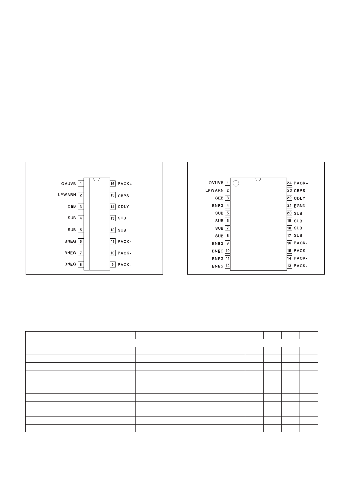
CONNECTION DIAGRAMS
SOIC-16 (Top View)
DP Package
TSSOP-24 (Top View)
PWP Package
3
UCC3958 -1/-2/-3/-4
ELECTRICAL CHARACTERISTICS:
Unless otherwise specified, PACK+ = 4V, –20°C < TA< 70°C. All voltages
measured with respect to BNEG. TA=T
J
.
PARAMETER TEST CONDITIONS MIN TYP MAX UNITS
BNEG/PACK - SWITCH
V
BNEG-VPACK
NORM, I
SWITCH
= 2A –100 –150 mV
NORM, I
SWITCH
= –2A 100 150 mV
V
PACK
+>VOV,I
SWITCH
= 20mA to 2A,
(OV State)
–100 –300 mV
V
PACK
+ = 2.5V, I
SWITCH
= –20mA to –2A,
(UV State)
100 600 mV
RDS
ON
NORM I
SWITCH
=2A 50 75 mΩ
NORM I
SWITCH
= –2A 50 75 mΩ
I
BNEG
– (Charger Leakage Current in OV) V
PACK
+>VOV(OV State)
([V
PACK
+]–[V
PACK
–]=6V)
120µA
BIAS Current
I
PACK
+V
PACK
+>V
UV
720µA
I
PACK
+ In Super Low Power Mode (V
PACK
+<VUV) 1 1.5 µA
V
BAT
Minimum Operating Cell Voltage 1.5 V
Battery Sample Rate (TS) 71217ms
Short Circuit Protection
ITHLD 2.75 5.25 7.25 A
TDLY CDLY = 0 350 µs
CDLY = 100pF
(Maximum Recommended Value)
2.5 ms
R
RESET
Overcurrent Reset Resistance 7.5 MΩ
LPWARN Output
LP Warn Threshold 2.55 2.65 2.75 V
TR C
LOAD
= 100pF, 10% to 90% of PACK+ 280 560 ns
TF C
LOAD
= 100pF, 10% to 90% of PACK+ 120 280 ns
V
HIGH(VPACK
+–V
LPWARN
)I
SINK
= 200µA, VUV<V
PACK
+<V
TLO
0.3 0.4 V
V
LOW
I
SOURCE
= 200µA, V
TLO<VPACK
+
<V
UV
0.3 0.4 V
Measure Delay 6ms
OVUVB Output
TR C
LOAD
= 100pF, Hi Z to 90% of PACK+ 280 560 ns
TF C
LOAD
= 100pF, Hi Z to 10% of PACK+ 140 280 ns
V
HIGH(VPACK
+
–V
OVUVB
)I
SOURCE
= 200µA, VPACK+ ≥ V
OV
0.3 0.4 V
V
LOW
I
SINK
=
200µA, VPACK+ ≤ V
UV
0.3 0.4 V
Z
OUT
Output Tristated 10 MΩ
Measure Delay 18 ms
CE Input
I
SINK
150 nA
Note 1: Other threshold voltages are available.

4
UCC3958 -1/-2/-3/-4
APPLICATION INFORMATION
Battery Voltage Monitoring
The battery cell voltage is sampled every 12ms by connecting a resistor divider across it and comparing the resulting voltage to a precision internal reference voltage.
Under normal conditions (cell voltage is below Over Voltage threshold and above Under Voltage threshold), the
UCC3958 consumes approximately 7µA of current and
the internal MOSFET is turned on with an R
DSON
of
50mΩ. The UCC3958 contains an on-chip Charge Pump
to ensure that the internal MOSFET gate is driven high
for complete turn-on, reducing power losses. The charge
pump switches and capacitors are all internal.
When the cell voltage falls below the Under Voltage
threshold for two consecutive samples, the IC disconnects the load from the battery pack and enters a super
low power mode (nominally 1µA). The pack will remain
in this state until it detects the application of a charger, at
which point controlled charging is enabled. The requirement of two consecutive readings below the UV threshold filters out momentary drops in cell voltage due to load
transients, preventing nuisance trips.
If the cell voltage exceeds the Over Voltage threshold for
two consecutive samples, charging is disabled, however
discharge current is still allowed. This feature of the IC is
explained further in the section on Controlled Charge/
Discharge Mode.
PIN DESCRIPTIONS
BNEG: Connect the negative terminal of the battery to
these pins.
CBPS: This power supply bypass pin is connected to
PACK+ through an internal 10k resistor. An external
capacitor must be connected between this pin and
BNEG. This capacitor functions as temporary charge
storage for high current conditions (short circuit).
Minimum capacitor value is 0.15µF. This value should be
increased if the CDLY cap is used.
CDLY: Delay control pin for the short circuit protection
feature. A capacitor connected between this pin and the
BNEG pin will increase the time delay for sensing an
over current condition. This adjustment may be useful in
those applications where high peak load currents may
momentarily exceed the protection circuit’s threshold and
interruption of the battery current would be undesirable.
The nominal delay time is set internally at 350µs
CEB: Chip Enable Bar. This pin is pulled low (wrt BNEG)
by a 100nA current source. In order to disable the IC, the
user must pull this pin high to PACK+.
LPWARN: Low Power Warning Indicator. This pin is
forced high when the battery voltage drops below V
TLO
(nominally 2.65V). This pin will stay high until the
detected battery voltage goes above V
TLO
,orUV
condition is declared.
OVUVB: This pin is an overvoltage/undervoltage
condition indicator. Under normal operating conditions
this pin is tristated. When an overvoltage (OV) state is
detected, this pin is pulled high. When undervoltage (UV)
condition is detected, this pin is pulled low.
PACK+: Connect to the positive terminal of the battery.
This pin is available to the user.
PACK-: These pins should be connected to the negative
terminal of the battery pack (negative terminal available
to the user). The internal FET switch connects this
terminal to the BNEG terminal to give the battery pack
user appropriate access to the battery.In an overcharged
state, only discharge current is permitted. In an
overdischarged state, only charge current is permitted.
SUB: Do not connect. These pins must be electrically
isolated from all other pins. These pins may be soldered
to isolated copper pads for heatsinking. This will improve
heat transfer, which may be necessary at high load
currents.
0.00
0.02
0.04
0.06
0.08
0.10
2.6
3.0 3.4 3.8 4.2
CELL VOLTAGE
OHMS
Figure 1. Typical Rdson vs Cell Voltage (DP Package
Pin 7 to Pin 10, at 25°C, 1 Amp Load)

5
UCC3958 -1/-2/-3/-4
Over Current Monitoring and Protection
Discharge current is continuously monitored via an internal sense resistor. In the event of excessive current, an
Over Current condition is declared if the high current
state persists for over 350µs. This delay allows for charging of the system bypass capacitors without tripping the
overcurrent. A delay of 350µs guarantees that the pack
can charge up to 680µF without declaring an Over Current condition. The delay may be extended to charge
larger load capacitors by connecting an external delay
capacitor from the CDLY pin to one of the BNEG pins.
Once an Over Current condition has been declared, the
internal MOSFET turns off. The only way to return the
pack to normal operation is to remove the load by unplugging the pack from the system. The overcurrent is reset when an internal pull down brings PACK– to within
less than 0.05V above BNEG. At this point, the pack returns to its normal state of operation. A capacitor on the
CBPS pin provides momentary holdup for the UCC3958
to assure proper operation in the event that a hard short
suddenly pulls the cell voltage below the minimum operating voltage. This cap value can be 0.15µF if the optional CDLY capacitor is not used. An internal 10k
resistor buffers the bypass capacitor from the Li-Ion cell.
System Status Indicators
The UCC3958 provides several convenient system monitoring signals. The first one is the Low Power Warning.
This output goes high when the cell voltage is less than
300mV above the Under Voltage Threshold. It signals
the system that the battery is getting close to its discharge limit.
The second monitoring signal is a tri-statable OV/UV output. Under normal operations conditions, this signal is
tri-stated. When an Over Voltage condition is declared,
the output is pulled high. When an Under Voltage condition is declared, the output is pulled low. This signal is
especially useful during test, allowing easy verification of
the OV and UV thresholds. These outputs are with respect to BNEG.
0
400
800
1200
1600
2000
4.0
5.0 6.0 7.0 8.0 9.0 10.0
CHARGER VOLTAGE (V)
LEAKAGE CURRENT (uA)
APPLICATION INFORMATION (continued)
Figure 2. Typical OV Leakage Current with Runaway
Charger at 25°C
Figure 3. State Diagram
UDG-98051
0
500
1000
1500
2000
2500
3000
0 20406080100
CDLYCAPVALUE(pf)
OC DELAY TIME (usec)
Figure 4. Typical Overcurrent Delay Time vs CDLY

6
UCC3958 -1/-2/-3/-4
Figure 6. SIngle Cell Lithium-Ion Battery Protector IC Application Diagram
UDG-97152
Controlled Charge/Discharge Mode
When the chip senses an over-voltage condition, it prevents any additional charging, but allows discharge. This
is accomplished by activating a linear control loop which
controls the gate of the MOSFET based on the differential voltage across its drain to source terminals. The linear loop attempts to regulate the differential voltage
across the MOSFET to 100mV. When a light load is applied to the part, the loop adjusts the impedance of the
MOSFET to maintain 100mV across it. As the load increases, the impedance of the MOSFET is decreased to
maintain the 100mV control. At heavy loads (still below
“over-current” limit level), the loop will not maintain regulation and will drive the gate of the MOSFET to the battery voltage (not the charge-pump output voltage). The
MOSFET R
DSON
in the over-voltage state will be slightly
higher than R
DSON
during normal operation. The voltage
drop (and associated power loss) across the internal
MOSFET in this mode of operation is lower than the typical solution of two external back-to-back MOSFETs,
where the body diode is conducting.
0
100
200
300
400
500
600
700
2.00
2.10 2.20 2.30 2.40
CELL VOLTAGE (V)
MOSFET VOLTAGE DROP (mV)
0.2Amp 1.0Amp 2.0Amp
Figure 5. Typical MOSFET Voltate Drop During
Charge in UV vs. Cell Voltage.
APPLICATION INFORMATION (continued)

7
UCC3958 -1/-2/-3/-4
UNITRODE CORPORATION
7 CONTINENTAL BLVD.• MERRIMACK,NH 03054
TEL. (603) 424-2410 • FAX (603) 424-3460
When the chip senses an under-voltage condition, it disconnects the load from the battery pack and shuts itself
down to minimize current drain from the battery. Several
circuits remain powered and will detect placement of the
battery pack into a charger. Once the charger presence
is detected, the linear loop is activated and the chip al-
lows charging current into the battery. This linear control
mode of operation is in effect until the battery voltage
reaches a level 300mV above the under-voltage threshold, at which time normal operation is resumed.
APPLICATION INFORMATION (continued)

IMPORTANT NOTICE
T exas Instruments and its subsidiaries (TI) reserve the right to make changes to their products or to discontinue
any product or service without notice, and advise customers to obtain the latest version of relevant information
to verify, before placing orders, that information being relied on is current and complete. All products are sold
subject to the terms and conditions of sale supplied at the time of order acknowledgement, including those
pertaining to warranty, patent infringement, and limitation of liability.
TI warrants performance of its semiconductor products to the specifications applicable at the time of sale in
accordance with TI’s standard warranty. Testing and other quality control techniques are utilized to the extent
TI deems necessary to support this warranty. Specific testing of all parameters of each device is not necessarily
performed, except those mandated by government requirements.
CERT AIN APPLICATIONS USING SEMICONDUCTOR PRODUCTS MAY INVOLVE POTENTIAL RISKS OF
DEATH, PERSONAL INJURY, OR SEVERE PROPERTY OR ENVIRONMENTAL DAMAGE (“CRITICAL
APPLICATIONS”). TI SEMICONDUCTOR PRODUCTS ARE NOT DESIGNED, AUTHORIZED, OR
WARRANTED TO BE SUITABLE FOR USE IN LIFE-SUPPORT DEVICES OR SYSTEMS OR OTHER
CRITICAL APPLICATIONS. INCLUSION OF TI PRODUCTS IN SUCH APPLICA TIONS IS UNDERSTOOD T O
BE FULLY AT THE CUSTOMER’S RISK.
In order to minimize risks associated with the customer’s applications, adequate design and operating
safeguards must be provided by the customer to minimize inherent or procedural hazards.
TI assumes no liability for applications assistance or customer product design. TI does not warrant or represent
that any license, either express or implied, is granted under any patent right, copyright, mask work right, or other
intellectual property right of TI covering or relating to any combination, machine, or process in which such
semiconductor products or services might be or are used. TI’s publication of information regarding any third
party’s products or services does not constitute TI’s approval, warranty or endorsement thereof.
Copyright 1999, Texas Instruments Incorporated
 Loading...