

Datasheet UCC3957MTR-3, UCC3957MTR-2, UCC3957MTR-1, UCC3957M-3, UCC3957M-2 Datasheet (Texas Instruments)
...
UCC3957 -1/-2/-3/-4
PRELIMINARY
SLUS236 - JANUARY 1999
FEATURES
• Three or Four Cell Operation
• Two Tier Overcurrent Limiting
• 30µA Typical Supply Current
Consumption
• 3.5µA Typical Supply Current in Sleep
Mode
• Smart Discharge Minimizes Losses in
Overcharge Mode
• 6.5V to 20V VDD Supply Range
• Highly Accurate Internal Voltage
Reference
• Externally Adjustable Delays in
Overcurrent Controller
• Detection of Loss of Cell Sense
Connections
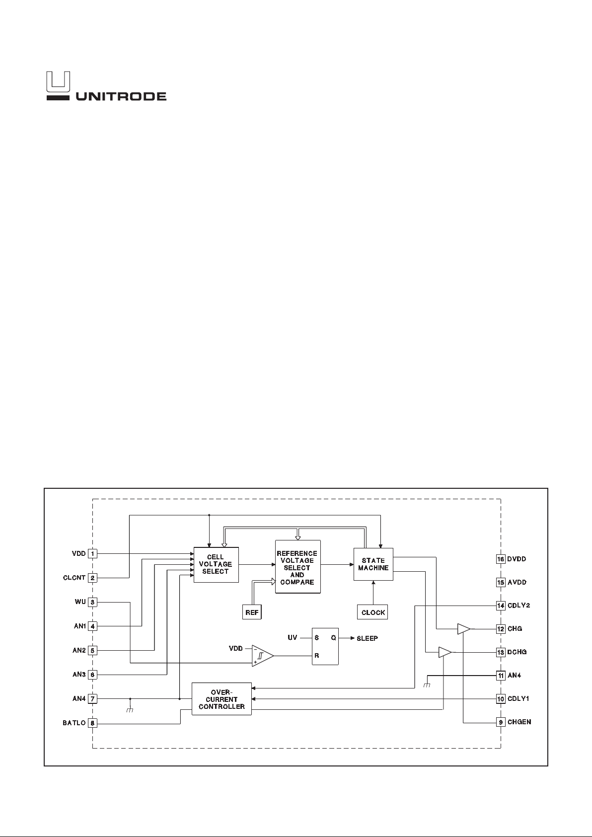
Three - Four Cell Lithium-Ion Protector Circuit
BLOCK DIAGRAM
UDG-97060
DESCRIPTION
The UCC3957 is a BiCMOS three or four cell lithium-ion battery pack
protector designed to operate with external P-channel MOSFETs. Utilizing external P-channel MOSFETs provides the benefits of no loss of
system ground in an overdischarge state, and protects the IC as well as
battery cells from damage during an overcharge state. An internal state
machine runs continuously to protect each lithium-ion cell from overcharge and overdischarge. A separate overcurrent protection block protects the battery pack from excessive discharge currents.
If any cell voltage exceeds the overvoltage threshold, the appropriate external P-channel MOSFET is turned off, preventing further charge current. An external N-channel MOSFET is required to level shift to this high
side P-channel MOSFET. Discharge current can still flow through the
second PFET. Likewise, if any cell voltage falls below the undervoltage
limit, the second P-channel MOSFET is turned off and only charge current is allowed. Such a cell voltage condition will cause the chip to go
into low power sleep mode. Attempting to charge the battery pack will
wake up the chip. A cell count pin (CLCNT) is provided to program the IC
for three or four cell operations.
A two tiered overcurrent controller and external current shunt protect the
battery pack from excessive discharge currents. If the first overcurrent
threshold level is exceeded, an internal timing circuit charges an external
capacitor to provide a user programmable blanking time.
(continued)
2
UCC3957 -1/-2/-3/-4
ELECTRICAL CHARACTERISTICS:
Unless otherwise specified, VDD = 16V and –20°C < TA< 70°C, TA= TJ.
All voltages measured with respect to the AN4 terminal.
PARAMETER TEST CONDITIONS MIN TYP MAX UNITS
Supply Section
Minimum V
DD
5.0 5.5 V
Supply Current 30 40 µA
Sleep Mode Supply Current VDD= 10.4V 3.5 7.5 µA
Output Section
DCHG Output Current Driving Logic Low and V
O
= 1V 40 70 100 µA
Driving Logic High and VO= VDD – 1 –20 –7 –3 mA
CHG Ouput Current Driving Logic Low and VO= 1V 40 70 100 µA
Driving Logic High and VO= VDD – 1V –20 –7 –3 mA
State Transitions
Normal to Overcharge UCC3957-1 4.15 4.20 4.25 V
Overcharge to Normal UCC3957-1 3.95 4.00 4.05 V
Normal to Overcharge UCC3957-2 4.20 4.25 4.30 V
Overcharge to Normal UCC3957-2 4.00 4.05 4.10 V
Normal to Overcharge UCC3957-3 4.25 4.30 4.35 V
Overcharge to Normal UCC3957-3 4.05 4.10 4.15 V
Normal to Overcharge UCC3957-4 4.30 4.35 4.40 V
Overcharge to Normal UCC3957-4 4.10 4.15 4.20 V
Undercharge to Normal 2.5 2.6 2.7 V
Normal to Undercharge 2.2 2.3 2.4 V
OV to CHG Delay (Note 1) 10 17 23 ms
ABSOLUTE MAXIMUM RATINGS
Supply Voltage . . . . . . . . . . . . . . . . . . . . . . . . . . . . . . . . . . 20V
Supply Current . . . . . . . . . . . . . . . . . . . . . . . . . . . . . . . . . 25mA
Output Current (CHG, DCHG) . . . . . . . . . . . . . . . . . . . . . 25mA
WU Input Voltage . . . . . . . . . . . . . . . . . . . . . . . . . . . . . . . . 28V
BATLO Input Voltage. . . . . . . . . . . . . . . . . . . . . . –0.3V to 2.5V
AN1 and AN3 Input Voltage . . . . . . . . . . . . . . . . . VAN4 – VDD
CLCNT and CHGEN. . . . . . . . . . . . . . . . . . . . . . . VAN4 – VDD
Storage Temperature . . . . . . . . . . . . . . . . . . . –65°C to +150°C
Junction Temperature. . . . . . . . . . . . . . . . . . . –55°C to +150°C
Lead Temperature (Soldering, 10 sec.). . . . . . . . . . . . . +300°C
Unless otherwise indicated, voltages are referenced to AN4.
Currents are positive into, negative out of the specified terminal.
Consult Packaging Section of Databook for thermal limitations
and considerations of packages.
DESCRIPTION (continued)
If at the end of the blanking time the overcurrent condition still exists, the external discharge FET is turned off
for a period 17 times longer than the first blanking period, and then the discharge FET is turned back on. If at
any time a second higher overcurrent threshold is ex-
ceeded for more than a user programmable time, the discharge FET is turned off, and will remain off for the same
period as the first tier off time. This two tiered overcurrent
protection scheme allows for charging capacitive loads
while retaining effective short circuit protection.
CDLY2
AVDD
DVDD
DCHG
CHG
CDLY1
AN4
CHGEN
1
2
3
4
5
6
7
8
16
15
14
13
12
11
10
9
CLCNT
VDD
BATLO
AN3
AN4
WU
AN1
AN2
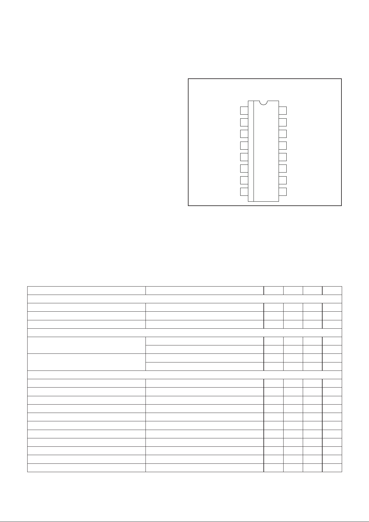
CONNECTION DIAGRAM
SSOP-16 (Top View)
M Package
3
UCC3957 -1/-2/-3/-4
PIN DESCRIPTIONS
AN1: Connects to the negative terminal of the top battery
cell and the positive terminal of the second battery cell.
AN2: Connects to the bottom terminal of the second
battery cell and the top terminal of the third battery cell.
AN3: Connects to the bottom terminal of the third battery
cell and the top terminal of the fourth battery cell in a four
cell stack. In a three cell pack it connects to the bottom
terminal of the third battery and to AN4.
AN4: Connects to the bottom terminal of the battery
stack and the top of the current sense resistor.
AVDD: Internal analog supply bypass cap pin. Connect a
0.1µF capacitor between this pin and AN4. This pin is
nominally 7.3V.
BATLO: Connects to the bottom of the current sense
resistor and the negative terminal of the battery pack.
CHGEN: The charge enable input for the protection IC.
This point must be driven high to allow charging of the
battery pack. This pin has a very weak pulldown.
CDLY1: Delay control pin for the short circuit protection
feature. A capacitor connected between this point and
AN4 will determine the time delay from when an
overcurrent situation is detected to when the FET is
turned off. This capacitor also controls the hiccup mode
timeout period.
CDLY2: An external cap can be tied between this pin
and AN4 to extend the blanking time on the second current limit tier.
CLCNT: This pin programs the IC for three or four cell
operation. Tying this pin low (to AN4) sets four cell operation, w`hile tying it high (to VDD or the preferred DSPLY
or ASPLY) sets three cell operation. This pin is internally
pulled low, so open circuit conditions will always result in
four cell mode.
DCHG: This pin is used to prevent overdischarge. If the
state machine indicates that any cell is undervoltage, this
pin will be driven high with respect to chip substrate so
that the external P-channel MOSFET will prevent further
discharge. If all cell voltages are above the minimum
threshold, this pin will be driven low.
CHG: This pin is used to control an external N-channel
MOSFET, which in turn drives a P-channel MOSFET. If at
least one cell voltage is over the OV threshold, this pin
will be driven low with respect to AN4. If all cell voltages
are below this threshold, this pin will be driven high.
DVDD: Internal digital supply bypass capacitor pin. Connect a 0.1µF capacitor between this pin and AN4. This
pin is nominally 7.3V.
VDD: Supply voltage to the IC. Connect this point to the
top of the lithium-ion battery stack.
WU: This pin is used to provide a wake up signal to the
IC during sleep mode. Connect this pin to the drain of the
N-channel level shift MOSFET.
ELECTRICAL CHARACTERISTICS: Unless otherwise specified, VDD = 16V and –20°C < T
A
< 70°C, TA= TJ.
All voltages measured with respect to the AN4 terminal.
PARAMETER TEST CONDITIONS MIN TYP MAX UNITS
State Transitions (continued)
UV to DCHG Delay (Note 1) 10 17 23 ms
Cell Sample Rate (Note 1) 5 8.5 11.5 ms
Smart Discharge Threshold BATLO Voltage 12 15 20 mV
Wakeup Input Threshold With Respect to V
DD 50 mV
Charge Enable Input Threshold 0.8 1.3 2.6 V
Short Circuit Protection
First Tier Threshold Level V
BATLO
120 150 180 mV
Second Tier Threshold Level V
BATLO
300 375 450 mV
First Tier Blanking Time CDLY1 = 0.1µF 305070ms
Restart Time CDLY1 = 0.1µF 300 500 700 ms
Second Tier Blanking Time CDLY2 = 10pF 200 400 550 µs
Note 1: Tested at probe only.
Note 2: Other OV/UV thresholds are available. Please consult the factory.

4
UCC3957 -1/-2/-3/-4
APPLICATION INFORMATION
Overview
The UCC3957 provides complete protection against
over-discharge, over-charge and overcurrent for a three
or four cell Lithium-Ion battery pack. It uses a “flying capacitor” technique to sample the voltage across each
battery cell and compare it to a precision reference. If
any cell is in over or under-voltage, the internal state machine takes the appropriate action to prevent further
charge or discharge. High-side P-MOSFETs are used to
independently control charge and discharge current. Typical application circuits are shown in Figures 1 and 2.
Connecting the Cell Stack
When connecting the cell stack to the circuit, it is important to do it in the proper order. First, the bottom of the
stack should be connected to AN4 . Next, the top of the
stack should be connected to VDD. The cell taps can
then be connected to AN1-AN3 in any order.
Choosing Three or Four Cells
For three cell packs, the cell count pin (CLCNT) should
be connected to the DSPLY pin, and the AN3 pin should
be tied to the AN4 pin. For four cell applications, the
CLCNT pin should be grounded (to AN4) and the AN3
pin will be connected to the positive terminal of the bottom cell in the stack.
Under-voltage Protection
When any cell is found to be over-discharged (below the
Normal to Undercharge threshold), the state machine
turns off both high-side FETs and enters the sleep mode,
where current consumption drops to about 3.5uA. It remains in sleep mode until the application of a charger is
sensed by the Wake Up (WU) pin being raised above
VDD.
Charging
Once a charger has been applied, the Charge FET will
be turned on as long as the Charge Enable input
(CHGEN) is pulled up to the DSPLY pin. If the CHGEN
input is left open (or connected to AN4), the Charge FET
will remain off.
During charge, the Discharge FET will be off (current will
be conducted through its body diode) until the cell voltages are all above the Undercharge to Normal threshold.
Once the cell voltages are above this threshold, the Discharge FET will be turned on, minimizing power dissipation.
Open Wire Protection
The UCC3957 provides protection against broken cell
sense connections within the pack. If the sense connection to one of the cells (pins AN1, 2 or 3) should become
disconnected, weak internal current sources will make
the cells connected to that wire appear to be in overcharge and charging of the pack will be prevented.
Over-voltage Protection and the “Smart Discharge”
Feature
If any cell is charged to a voltage exceeding the Normal
to Overcharge threshold, the Charge FET will be turned
off, preventing further charge current. Hysteresis keeps
the Charge FET off until the cell voltages have dropped
below the Overcharge to Normal threshold. In most protector designs, the Charge FET is held off completely
within this voltage band. During this time, discharge current must be conducted through the body diode of the
Charge FET. This forward voltage drop can be as high as
1V, causing significant power dissipation in the Charge
FET and wasting precious battery power.
The UCC3957 has a unique “Smart Discharge” feature
that allows the Charge FET to come back on (for discharge only) while still in the overcharge hysteresis band.
This greatly reduces power dissipation in the Charge
FET. This is accomplished by sensing the voltage drop
across the current sense resistor. If this drop exceeds
15mV (corresponding to 0.6 amps of discharge current
using a .025 sense resistor), the Charge FET is turned
back on. This threshold assures that only discharge current will be conducted. In an example using a 20m FET
with a 1V body diode drop and a 1 amp load, the power
dissipation in Q1 would be reduced from 1 watt to 0.02
watts. Note that a similar technique is not used during
charge (when the Discharge FET is off due to cells being
in undervoltage) because the charge current should be
low while the cells are in undervoltage.
Protection Against a Runaway Charger
The use of a small N-channel level shifter (Q3 in the application diagrams) allows the IC to interface with the
high-side Charge FET (Q1), even in the presence of a
runaway charger. Only the drain-source voltage rating of
the charge FET limits the charge voltage that the protection circuit can withstand. The Wakeup (WU) pin is designed to handle input voltages greater than VDD, as
long as the current is limited. In the examples shown, the
Charge FET’s gate-source resistor (R1) provides this
current limiting. Note that in Figure 2, a resistor and
zener (R2 and VR1) have been added to protect Q1
against any possibility of a voltage transient exceeding
its maximum gate-source rating.
Overcurrent Protection
The UCC3957 protects the battery pack from an overload or a hard short circuit using a two-tier overcurrent
protection scheme. The overcurrent protection is de-

5
UCC3957 -1/-2/-3/-4
1
2
3
4
5
6
7 10
98
16
15
14
13
12
11
DVDD
VDD
CLCNT
WU
AN1
AN2
AN3
AN4
BATLO
CHGE
N
AN4
CHG
DCHG
CDLY2
AVDD
CDLY1
R1
1MEG
Q2
IRF7416
Q1
IFR7416
Q3
2N7002
C4
0.022µF
C3
OPTIONAL
C1
0.1µF
C2
0.1µF
R
SENSE
.025Ω
S1
LI-ION BATTERY STACK
PACK (–)
PACK (+)
CLOSE TO
ENABLE CHARGING
"CHARGE"
"DISCHARGE"
D1
1A, 50V
C5
4.7µF
25V
+
Figure 1. Three cell lithium-ion protector application diagram, showing optional charge enable switch.
Note: D1 protects Q2 from inductive kick at turn-off.
UDG-98016
1
2
3
4
5
6
7 10
98
16
15
14
13
12
11
DVDD
VDD
CLCNT
WU
AN1
AN2
AN3
AN4
BATLO
CHGEN
AN4
CHG
DCHG
CDLY2
AVDD
CDLY1
R1 1MEG
R2
10K
Q2
IRF7416
Q1
IFR7416
Q3
2N7002
VR1 18V
C4
0.022µF
C3
OPTIONAL
C1
0.1µF
C2
0.1µF
R
SENSE
.025Ω
LI-ION BATTERY STACK
PACK (–)
PACK (+)
"CHARGE"
"DISCHARGE"
D1
1A, 50V
C5
4.7µF
25V
+
Figure 2. Four cell protector with optional components to protect the charge FET from excessive gate-source
transients.
Note1. VR1 and R2 are optional. They protect Q1 from excessive open-circuit charger voltage.
Note 2. D1 protects Q2 from inductive kick at turn-off.
UDG-98017

6
UCC3957 -1/-2/-3/-4
0.1
1
10
100
1000
0.001 0.01 0.1
CDLY1 (µF)
DELAY TIME (msec)
Delay Off Time
Figure 3. Typical tier 1 Overcurrent delay time and
off time vs. CDLY1.
APPLICATION INFORMATION (continued)
0
200
400
600
800
1000
1200
1400
0 10203040
CDLY2 (pf)
DELAY T IME (
µ
sec)
Figure 4. Typical tier 2 Overcurrent delay time vs.
CDLY2.
signed to go into a hiccup mode when the voltage drop
across an external sense resistor (connected to the AN4
and BATLO pins) exceeds a certain threshold. In this
mode, the Discharge FET is periodically turned off and
on until the fault is removed. Once the fault is removed,
normal operation is automatically resumed.
To facilitate charging large capacitive loads, there are
two overcurrent threshold voltages, each with its own
user programmable time delay. This two-tier approach
provides fast response to short circuits, while enabling
the battery pack to provide short duration surge currents.
It also facilitates the charging of large filter caps without
causing nuisance overcurrent trips.
The first tier threshold is 150mV nominal, corresponding
to 6 amps using a .025 sense resistor as shown in the
examples of Fig’s1&2.Ifthepack discharge current exceeds this amount for a period of time, determined by the
capacitor on the CDLY1 pin, then the hiccup mode will be
entered. The first tier hiccup duty cycle is fixed at approximately 6%, minimizing power dissipation in the event of
a sustained overload. The absolute on and off times of
the Discharge FET (Q2) are controlled by the CDLY1 capacitor. A curve relating the delay (on) time to this capacitor value is shown in Figure 3. The off time is
approximately 17 times longer than the on time.
The second tier overcurrent threshold is nominally
375mV, corresponding to 15 amps using a .025 sense
resistor. If the pack current exceeds this value for a period of time, determined by the capacitor on the CDLY2
pin, then the hiccup mode will be entered with a much
lower duty cycle, typically less than 1%. The relationship
of this time delay (on time) to the CDLY2 capacitor value
is shown in the curve of Figure 4. The off time during this
hiccup mode is still determined by the CDLY1 capacitor,
as previously described. This technique greatly reduces
the stress and power dissipation in the FETs during short
circuit conditions.
In the examples shown in Fig’s1&2(with
CDLY1=.022 F), the first tier overcurrent on time will be
about 10msec, while the off time will be about 170msec,
resulting in a 5.9% duty cycle for currents over 6 amps
(but less than 15 amps). If no CLDY2 capacitor is used,
the second tier on time will be less than 200 sec (assuming no stray capacitance), resulting in a duty cycle of
about 0.1% for currents over 15 amps. If CDLY2=22pF,
the typical on time for currents exceeding 15 amps will
be about 800usec, resulting in a duty cycle of 0.5%.
Protecting Against Inductive Kick at Turn-off
In the case of a short circuit, the di/dt that occurs when
the Discharge FET is turned off can result in a significant
voltage undershoot at the pack output due to stray inductance. This undershoot can potentially exceed the breakdown voltage rating of the Discharge FET. A clamp diode
(D1 in Fig’s 1, 2 & 3), or a capacitor across the pack output, protects against this possibility. A diode also provides protection from a reverse polarity charger.
During turn-off, a voltage overshoot can occur at the top
of the cell stack, due to wiring inductance and the cells’
internal ESL (Equivalent Series Inductance). During very
high di/dt conditions, such as that which occurs when
turning off in response to a short circuit, this voltage
overshoot can be significant and potentially damage the

7
UCC3957 -1/-2/-3/-4
1
2
3
4
5
6
7 10
98
16
15
14
13
12
11
DVDD
VDD
CLCNT
WU
AN1
AN2
AN3
AN4
BATLO
CHGEN
AN4
CHG
DCHG
CDLY2
AVDD
CDLY1
R1 1MEG
R2
10K
Q2
IRF7416
Q1
IFR7416
Q3
227002
VR1 18V
C4
0.022µF
C1
0.1µF
C2
0.1µF
R
SENSE
.025Ω
LI-ION BATTERY STACK
PACK (–)
PACK (+)
"CHARGE"
"DISCHARGE"
D1
1A, 50V
R3
1K
C5
0.22µF
R4
100
C6
.22µF
Figure 5. Four cell protector with slew rate limiting the discharge FET.
Note 1: VR1 and R2 are optional. They protect Q1 from excessive open-circuit charger voltage.
Note 2. R3 and C5 are chosen based on capacitive load that must be driven.
Note 3. R4 minimizes inductive kick at turn-off.
APPLICATION INFORMATION (continued)
UDG-98018
IC or the Discharge FET (Q2). For this reason, it is
strongly recommended that a capacitor (C5 in Fig’s 1 &
2) be placed across the cell stack, from VDD to AN4, and
that stray inductance be minimized in the battery current
path. An alternative to adding a capacitor across the cell
stack is to reduce the di/dt. This is discussed in the next
section.
Controlling Discharge FET Turn-on / Turn-off Times
By slew rate limiting the pack output voltage at turn-on,
the surge current into large capacitive loads can be
greatly reduced.
This allows the designer to select shorter overcurrent delay times, minimizing the stress on Q1 and Q2 in the
event of a shorted pack output. A simple method of implementing slew rate limiting is shown in Figure 5. It consists of an RC network (R3 and C5) between gate and
drain of the Discharge FET (Q2) to control its turn-on
time. This circuit relies on the relatively high sink impedance (about 20K) of the UCC3957’s DCHG output. The
values shown for R3 and C5 will provide a pack output
voltage rise time of about 4.5msec when the Discharge
FET (Q2) is turned on. Note that the addition of R3 and
C5 has made it possible to eliminate the CDLY2 capacitor, for the quickest response to a true short circuit. While
this circuit will not prevent a large surge current when inserting a “live” battery pack into a highly capacitive load,
it will allow it to restart (after one hiccup cycle) if this initial surge current trips the overcurrent protection.
Increasing the turn-off time of the Discharge FET (Q2)
reduces the inductive kick that results during turn-off after an overcurrent condition. This is accomplished by
adding a resistor (R4) in series with the DCHG output.
This reduction of di/dt at turn-off will minimize (or eliminate) the need for a capacitor across the battery stack. It
is recommended that this resistor value not exceed a few
hundred ohms, or the ability to turn off quickly enough
into a short may be compromised.
Due to the relatively low charge currents (typically a few
amps max), controlling the turn-on and turn-off times of
the Charge FET is not beneficial. In fact, the turn-off time
of the Charge FET will be slow due to the large value of
R1, the gate-source resistor.
UNITRODE CORPORATION
7 CONTINENTALBLVD. • MERRIMACK, NH 03054
TEL. (603) 424-2410 • FAX (603) 424-3460

IMPORTANT NOTICE
T exas Instruments and its subsidiaries (TI) reserve the right to make changes to their products or to discontinue
any product or service without notice, and advise customers to obtain the latest version of relevant information
to verify, before placing orders, that information being relied on is current and complete. All products are sold
subject to the terms and conditions of sale supplied at the time of order acknowledgement, including those
pertaining to warranty, patent infringement, and limitation of liability.
TI warrants performance of its semiconductor products to the specifications applicable at the time of sale in
accordance with TI’s standard warranty. Testing and other quality control techniques are utilized to the extent
TI deems necessary to support this warranty. Specific testing of all parameters of each device is not necessarily
performed, except those mandated by government requirements.
CERT AIN APPLICATIONS USING SEMICONDUCTOR PRODUCTS MA Y INVOLVE POTENTIAL RISKS OF
DEATH, PERSONAL INJURY, OR SEVERE PROPERTY OR ENVIRONMENTAL DAMAGE (“CRITICAL
APPLICATIONS”). TI SEMICONDUCTOR PRODUCTS ARE NOT DESIGNED, AUTHORIZED, OR
WARRANTED TO BE SUITABLE FOR USE IN LIFE-SUPPORT DEVICES OR SYSTEMS OR OTHER
CRITICAL APPLICATIONS. INCLUSION OF TI PRODUCTS IN SUCH APPLICA TIONS IS UNDERSTOOD T O
BE FULLY AT THE CUSTOMER’S RISK.
In order to minimize risks associated with the customer’s applications, adequate design and operating
safeguards must be provided by the customer to minimize inherent or procedural hazards.
TI assumes no liability for applications assistance or customer product design. TI does not warrant or represent
that any license, either express or implied, is granted under any patent right, copyright, mask work right, or other
intellectual property right of TI covering or relating to any combination, machine, or process in which such
semiconductor products or services might be or are used. TI’s publication of information regarding any third
party’s products or services does not constitute TI’s approval, warranty or endorsement thereof.
Copyright 1999, Texas Instruments Incorporated
 Loading...