

1/98
FEATURES
• Precision 4.1V Reference (1%)
• High Efficiency Battery Charger Solution
• Average Current Mode Control from
Trickle to Over Charge
• Resistor Programmable Charge Currents
• Internal State Logic Provides Four
Charge States
• Programmable Over Charge Time
• Fully Differential Switch Mode Current
Sensing
• CHG Pin Initiates Charging
Switch Mode Lithium-Ion Battery Charger Controller
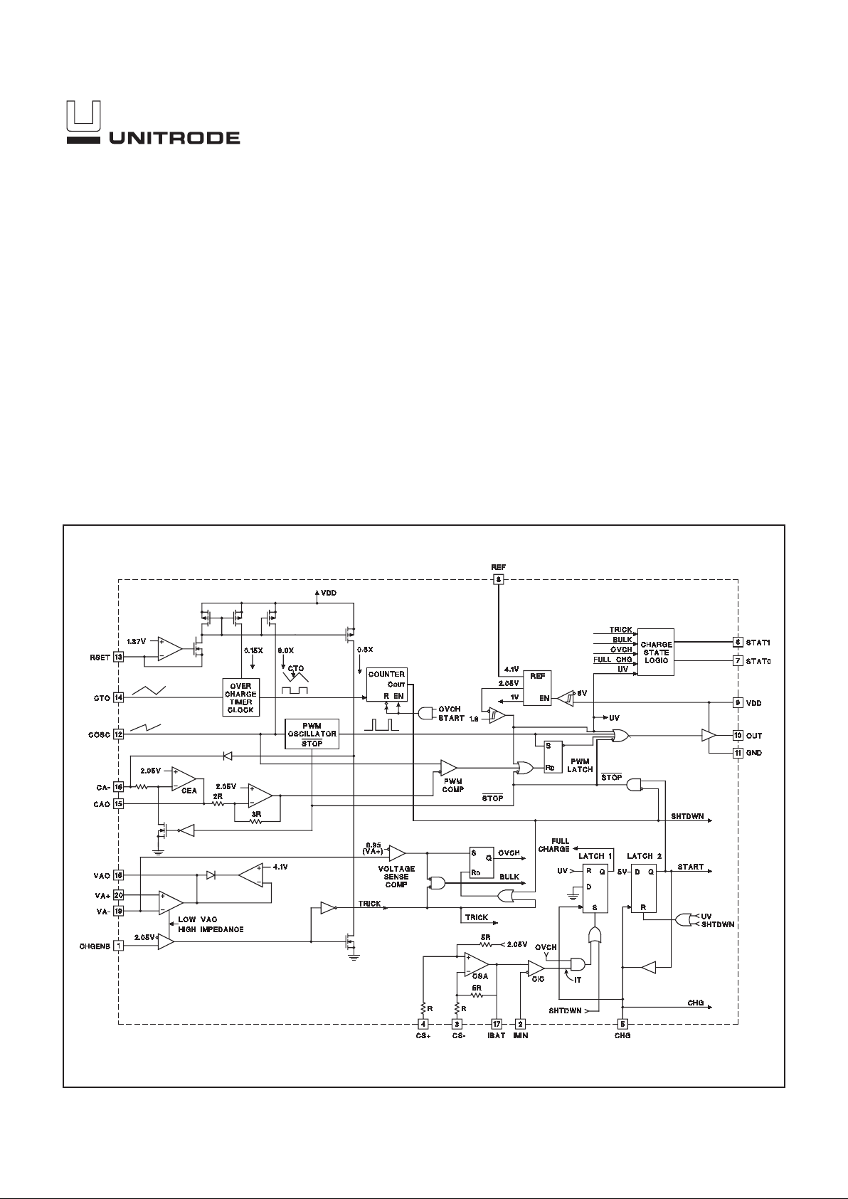
BLOCK DIAGRAM
UDG-96197-1
UCC2956
UCC3956
PRELIMINARY
DESCRIPTION
The UCC3956 family of Switch Mode Lithium-Ion Battery Charger
Controllers accurately control lithium-ion battery charging with a
highly efficient average current control loop.This chip is designed to
work as a stand alone charger controller for a single cell or multiple
cell battery pack. This chip combines charge state logic and average current PWM control circuitry with a 14 bit counter to program
the over charge time. The charge state logic indicates current or
voltage control depending on the charge state. The chip includes
undervoltage lockout circuitry to insure sufficient supply voltage is
present before output switching starts. Additional circuit blocks include a differential current sense amplifier, a 1% voltage reference,
voltage and current error amplifiers, PWM latch, charge state decode bits, and a 500mA output driver.
2
UCC2956
UCC3956
ELECTRICAL CHARACTERISTICS: Unless otherwise specified, TA = –40°C to +85 for UCC2956 and 0°C to +70°C for
UCC3956, COSC = 500pF, RSET = 70k, CTO = 169nF, VDD = 12V, TA =TJ.
PARAMETER TEST CONDITIONS MIN TYP MAX UNIT
Current Sense Amplifier (CSA)
DC Gain CS– = 0, CS+ = –50mV and CS+ = –250mV 4.9 5 5.1 V/V
CS+ = 0, CS– = 50mV and CS– = 250mV 4.9 5 5.1 V/V
CAO CS+ = CS– = 0V 1.99 2.05 2.11 mV
CMRR V
CM = 1.1V to 18V, VDD = 18V 50 65 dB
VOL CS+ = –0.2V, CS– = 0.5V, IO = 1mA 0.3 V
V
OH CS+ = 0.5V, CS– = –0.2V, IO = –500µA 3.7 4.1 4.4 V
Output Source Current IBAT = 3V, VID = 700mV –500 µA
Output Sink Current IBAT = 1V, VID = –700mV 500 µA
3dB Bandwidth V
CM = 0V, CS+ - CS– = 100mV (Note 2) 0.1 3 MHz
Current Error Amplifier (CEA)
IB 8V < V
DD< 18V, CHGENB = REF 0.1 0.5 µA
CA– Voltage 8V < V
DD < 18V, CAO = CA– 1.99 2.05 2.11 V
AVO 60 90 dB
GBW T
J = 25°C, F = 100kHz 1 3 MHz
V
OL IO = 250µA, CA– = 3V 0.5 V
VOH IO = –1mA, CA– = 2V 3.7 4.1 4.4 V
I
CA–, Itrck_control VCHGENB = GND 8 10 12 µA
Voltage Error Amplifier (VEA)
IB Total Bias Current; Regulating Level 0.5 3 µA
VIO 8V < V
DD < 18V, –0.2 < VCM < 5V 10 mV
AVO 60 90 dB
GBW T
J = 25°C, F = 100kHz 0.75 3 MHz
VOL IO = 500µA, VA– = 3.8V 0.2 1 V
V
OH IO = –500µA, VA– = 4.4V 3.8 4.1 4.3 V
VAO Leakage V
CHGENB = GND, STAT0 = 0 and STAT1 = 0, VAO = 2.05V –1 1 µA
Pulse Width Modulator
Maximum Duty Cycle CAO = 0.5V 85 92 100 %
Modulator Gain CAO = 1.7V, 2.1V 57 64 71 %/V
ABSOLUTE MAXIMUM RATINGS
Supply Voltage VDD, OUT .........................20V
Output Current Sink
Continuous ................................120mA
Peak .....................................600mA
Output Current Source
Continuous ................................120mA
Peak .....................................600mA
CS+, CS–
Voltage ...............................–0.5 to VDD
Current with CS+, CS– less than –0.5.............50mA
Remaining Pin Voltages .....................–0.3V to 6V
Storage Temperature ...................–65°C to +150°C
Junction Temperature...................–55°C to +150°C
Lead Temperature (Soldering, 10 sec.).............+300°C
Currents are positive into, negative out of the specified terminal. Consult Packaging Section of Databook for thermal limitations and considerations of packages.
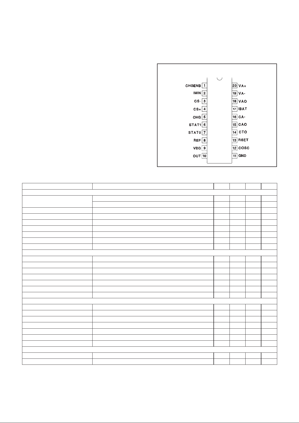
CONNECTION DIAGRAM
DIP-20, SOIC-20 (Top View)
JorN,DWPackages

3
UCC2956
UCC3956
ELECTRICAL CHARACTERISTICS: Unless otherwise specified, TA = –40°C to +85 for UCC2956 and 0°C to +70°C for
UCC3956, COSC = 500pF, RSET = 70k, CTO = 169nF, VDD = 12V, TA =TJ.
PARAMETER TEST CONDITIONS MIN TYP MAX UNIT
PWM Oscillator (OSC)
Frequency 7V < V
DD < 18V 90 100 110 kHz
Over Charge Timer (OCT)
Frequency 7V < V
DD < 18V (Note 1) 4.65 5 5.35 Hz
Reference
Initial Accuracy T
J = 25°C 4.06 4.1 4.14 V
Accuracy 0 < T
J < 70°C, VDD = 8V to 18V 4.05 4.1 4.15 V
Load Regulation 0 < I
O < 2mA 3 15 mV
Accuracy –40°C < T
J < 85°C, VDD = 8V to 18V 4.03 4.1 4.17 V
Short Circuit I REF = 0V 8 20 30 mA
Charge Enable Comparator (CEC)
Threshold Voltage 1.9 2.05 2.15 V
Input Bias Current –0.5 –0.2 µA
Voltage Sense Comparator (VSC)
Threshold Voltage Volts below VA+ 50 125 200 mV
Charge Current Comparator (CIC)
Threshold Voltage CS+ = CS– = 0, Function of IBAT = 2.05V 2 2.05 2.1 V/V
Input Bias Current Total Bias Current; Regulating Level –0.5 –0.2 µA
Output Stage
V
OL IO = 10mA 0.1 0.3 V
V
OH, Volts Below VDD IO = –10mA 0.1 0.5 V
Rise Time COUT = 1nF 30 70 ns
Fall Time C
OUT = 1nF 30 70 ns
STAT0 and STAT1 Open Drain Outputs
Maximum Sink Current V
OUT = 12V 15 30 mA
V
OL IOUT = 1mA 0.1 0.2 V
Charge Control (CHG)
Threshold Voltage 1.5 1.8 2.1 V
Charge Pin Pull Down
Resistance
3.0 5.0 kΩ
UVLO Section
Turn-on Threshold 6.0 6.5 6.75 V
Hysteresis 100 150 400 mV
IDD
IDD (Run) 58mA
IDD (UVLO) V
DD = 5V 0.25 0.75 mA
PIN DESCRIPTIONS
CA–: The inverting input to the current error amplifier.
CAO: The output of the current error amplifier and invert-
ing input of the PWM comparator. This pin is driven high
during shutdown.
CS–, CS+: The inverting and non-inverting inputs to the
current sense amplifier. This amplifier has a fixed gain of
5.
CHG: A rising edge triggered input pin that indicates
charging. Once the internal 14 bit timer has timed out the
chip enters its shutdown charge state. At this point CHG
is pulled low by an internal buffer. Another low to high
transition is required to reset the timer and restart charging.
CHGENB: The input to a comparator that detects when
the battery voltage is low and places the charger in
trickle charge. The charge enable comparator forces the
output of the voltage error amplifier to a high impedance
state while forcing a fixed 10µA current into the CA– to
set the trickle charge.
COSC: The oscillator ramp pin which has a capacitor
(COSC) to ground. The ramp oscillates between 0.8V to
3.2V and the frequency is determined by:

4
UCC2956
UCC3956
Frequency =
3.475
(COSC+ 20pF) RSET
A rising edge on CHG initiates the oscillator.
CTO: The slow oscillator ramp pin which is used to gen-
erate a clock signal for the 14 bit timer to program the
over charge time. A capacitor to ground is charged and
discharged with equal currents at a frequency programmed between 0.75Hz to 5Hz. The ramp oscillates
between 1.0V to 3.0V and the frequency is determined
by:
Frequency =
0.06
CTO RSET
The oscillator operates only while in overcharge.
GND: The reference point for the internal reference, all
thresholds, and the return for the remainder of the device.
IBAT: The output of the current sense amplifier.
IMIN: The minimum charge current programming pin is
provided to program an optional charge termination in
addition to the programmable timer.
OUT:The output of the PWM driver.
REF: The 4.1V precision reference which should be by-
passed with a 0.1µF capacitor.
RSET: This pin programs the charge current for the oscillator ramp. The oscillator charge current is determined
by:
1.37V
RSET
.
The trickle control current (Itrck_control) is determined
by:
0.68V
RSET
.
STAT0, STAT1: CMOS open drain binary output decode
pins indicating the four different charge states. The maximum high voltage sense comparator.
VA–: The inverting input to the voltage error amplifier that
is used as a battery sense input. It is also the input to the
voltage sense comparator. The bulk charge state is completed and over charge state is initiated when VA–
reaches 95% of VA+.
VA+: The non-inverting input to the voltage error amplifier that is used as the battery charge reference voltage.
VAO: The output of the voltage error amplifier. The upper
output clamp of this amplifier is 4.1V.
VDD: The input voltage of the chip. This chip is operational between 6V and 18V and should be bypassed with
a 0.1µF capacitor.
PIN DESCRIPTIONS (cont.)
STAT1 STAT0
Trickle Charge 0 0 CHGENB < 2.05V
Bulk Charge 0 1 VA– < 95% VA+ and CHGENB > 2.05V
Over Charge 1 0 VA– > 95% VA+ and VIBAT<VIMIN
Over Charge (Top Off) 1 1 VIBAT >VIMIN
CHARGE STATE DECODE CHART
APPLICATION INFORMATION
The UCC3956 contains all the necessary control functions for implementing an efficient switch mode LithiumIon battery charger. Lithium-Ion batteries are rapidly becoming the battery of choice for rechargeable portable
and lap top products. When compared to NiCd, NiMH,
and Lead Acid batteries, Lithium-Ion offer less weight
and volume for the same energy.Lithium-Ion batteries do
not suffer from the memory effect found in NiCd batteries.
This effect, caused by not completely discharging and
charging a battery, will reduce battery capacity over several charge cycles. Because Lithium-Ion batteries have a
high average cell voltage of around 3.6V, they can often
replace 2 to 3 Nickel based cells.
The advantages that Lithium-Ion batteries offer come at
the cost of a wide operating voltage. Near zero capacity,
the cell will typically have a voltage of 2.5V. A fully
charged cell will typically have a voltage of 4.1V. Unlike
many so called “smart” or “universal” chargers, the
UCC3956 is optimized for Lithium-Ion characteristics. In
order to restore capacity quickly, the chip features both
constant current and constant voltage modes of operation. A programmable over charge time, provided by the
UCC3956 timer, allows the charger to predictably restore
100% capacity to the battery.
Charger Operation
When CHG is transitioned from a low to high logic level,
the chip will cycle through several charge states. If the
battery voltage is severely depleted, the charger will begin in a low current trickle charge state. When the bat-

5
UCC2956
UCC3956
APPLICATION INFORMATION (cont.)
tery voltage is above a user set threshold, the charger
will initiate a constant current bulk charge state. Once the
battery reaches 95% of it’s final voltage, the charger will
enter an over charge state. During the over charge state,
the converter will transition from a constant current to a
constant voltage mode of operation. Figure 2 shows typical current, voltage, and capacity levels of a Lithium-Ion
battery during a complete charge cycle.
A Block Diagram of the UCC3956 is shown on the first
page of the data sheet, while Figure 1 shows a typical
application circuit for a Buck derived switch mode
charger.The UCC3956 can be used for charging a single
cell or multiple cells in series. If more than two cells are
stacked in series, however, a level shifting gate drive will
be needed to operate the buck switch. The application
circuit charges a 1200mAh 2 cell stack at a 1C rate.
Setting the Oscillator Frequency
The frequency of operation for the converter is set by
picking values for RSET and COSC.
fOSC =
3.475
(COSC+ 20pF) RSET
The UCC3956 is capable of operating at frequencies
higher than 200kHz. However, the actual operating frequency of the buck converter will ultimately be determined by the usual tradeoffs of size, cost and efficiency.
The application circuit frequency is set at 100kHz with
COSC = 180pF and RSET = 162k.
Trickle Charge State
When the battery’s voltage is below a predetermined
threshold, the battery is either deeply discharged or has
shorted cells. The trickle charge state offers a low charging current to bring the battery up above zero capacity.In
the case of shorted cells, the trickle charge state prevents the charger from delivering high currents during
this fault condition. Stacking several cells makes the detection of a shorted cell more difficult.
For Lithium-Ion batteries, the trickle charge threshold is
typically set to a value around 2.5V per cell (this corresponds to near zero capacity). When the cell voltage is
below the threshold, only a trickle current will be applied
to the battery. The threshold is established by programming CHGENB to 2.05V when the battery (or stack) voltage is at the threshold.Referring to the application circuit
Figure 1. Typical Application Circuit
UDG-96198-1
IBULK = 1.2A
ITRICKLE =90mA
f
OSC = 100kHz
Timeout = 120 minutes

6
UCC2956
UCC3956
APPLICATION INFORMATION (cont.)
of Figure 1, the trickle charge voltage threshold is determined by:
VTRICKLE_ THRESHOLD =
RS1+ RS2+ RS3
RS3
2.05
With a trickle threshold of 5V (for 2 cells) and setting RS3
to 10k, RS1+ RS2 should be approximately 14.4k.
The applications circuit trickle charge current is set to
about 7.5% of the bulk charge current. The current value
is set by picking the appropriate value for RG1. Referring
to the Block Diagram and Figure 1, during trickle charge
a fixed current
0.68
RSET
flows out of the current amplifier’s inverting input and into
RG1. The voltage amplifier output is disabled during
trickle charge and acts as a high impedance node. The
resulting voltage at the output of the current sense am-
plifier sets the trickle charge current.
ITRICKLE =
RG1
7.5 RSET RSENSE
In the application circuit the sense resistor is 0.18Ω and
R
SET is 162k, for a trickle current of about 90mA a 20k
resistor is selected for RG1.
The converter is typically designed to run in discontinu-
ous conduction mode during trickle charge. This allows a
reasonably small value of inductance to be used. The average current mode of the UCC3956 provides improved
discontinuous duty cycle control, when compared to peak
current mode implementations.
In Figure 2, the trickle charge state corresponds to the
time interval between t0 (when CHG is transitioned from
low to high) and t1.During the trickle charge state STAT0
and STAT1 are logic level lows. At time t1 the trickle
threshold is met, and the charger transitions to the bulk
charge state. In many instances, the battery voltage will
initially be above the trickle threshold. In this case, the
trickle charge state will not be needed.
Bulk Charge State
As the name implies, the bulk charge state is responsible
for restoring a majority of the charge back into the battery. The bulk charge current is determined by the C
rate and the capacity of the battery. In the application circuit, 2 stacked 1200mAH batteries are charged at a 1C
rate. This will require 1.2A of current during bulk
charge. In this case, a fully discharged battery will take
about 60 minutes to reach approximately 80% capacity.
Battery packs with a high ESR will typically have a
shorter bulk period, due to the voltage drop generated by
the bulk current and the ESR of the battery.
Both the voltage and current sense amplifiers are enabled during bulk charge. The voltage amplifier is saturated in this state as the battery voltage is slowly rising,
but is not yet high enough to drive the voltage amplifier
into regulation. The output of voltage amplifier is clamped
at a nominal voltage of 4.1V. The current sense amplifier
is configured such that its output voltage increases with
decreasing R
SENSE current. RSENSE should be sized
such that the output voltage of the current sense amplifier V
IBAT is within specification during bulk charge.
VIBAT(BULK) = 2.05 - 5 IBULK RSENSE
With 1.2A of bulk current and setting the current sense
amplifier output at 1V, a sense resistor of 0.18Ω is required. As always, power dissipation and converter efficiency must be considered when choosing R
SENSE.
Referring to the Feedback Diagram of Figure 3, the output of the voltage and current sense amplifiers are
summed together at the inverting input of the current amplifier. Assuming that the current amplifier is within regulation, the required value of RG2 can be calculated. The
application circuit uses a value of 38.3k for RG2, setting
the bulk current to 1.2A.
RG2 =
2.05 RG1
5 IBULK RSENSE
Referring to Figure 2, the bulk charge state corresponds
Figure 2. Typical Charge Cycle Levels
UDG-96262-1

7
UCC2956
UCC3956
APPLICATION INFORMATION (cont.)
to the interval between t1 and t2. The step in voltage at
time t1 is caused by bulk current flowing into the battery
ESR and sense resistor. In the bulk charge state STAT0
is a logic level high and STAT1 is a logic level low.
Over Charge State
The over charge state of the converter starts when the
battery reaches 95% of its final voltage (time t2 of Figure
2). The over charge state is initiated when the voltage at
the inverting input of the voltage amplifier is 95% of the
non-inverting input voltage.Using 95% rather than 100%
of the final battery voltage assures that the over charge
timer will always be set, before the battery current tapers
off. At the beginning of over charge STAT0 indicates a
logic level low and STAT1 indicates a logic level high.
In the application circuit of Figure 1, the voltage at which
over charge is initiated is set by resistors RS1, RS2 and
RS3. These resistors are also used to set the trickle
charge threshold. A 0.1µF decoupling capacitor is added
to this node as a filter. The battery (or stack) voltage that
will initiate the over charge state is:
VOC_ THRESHOLD = 0.95
RS1+ RS2+ RS3
RS2+ RS3
4.1
For a single cell stack, RS1 should be 0Ω. This results in
a final battery voltage of 4.1V. It is important not to
charge a Lithium-Ion battery above 4.2V. When charging
a battery stack, RS1 should be selected to properly set
the final stack voltage. In the application circuit, RS1 is
selected to be 12.21k and RS2 is selected to be 2.21k.
This sets the over charge level at 8.2V, while setting the
trickle charge threshold to about 5V.
The battery voltage at the beginning of the over charge
state may not correspond to the voltage amplifier coming
out of saturation. Therefore, bulk current may continue in
the battery during the initial portion of the over charge
state (see Figure 2). When the voltage amplifier comes
into regulation, the amplifier’s output voltage will begin to
decrease. The current sense amplifier’s output voltage
will need to increase, in order for the current amplifier’s
inverting input to remain at 2.05V. This will translate into
a decreasing battery current. The battery current will continue to decrease as the battery approaches 100% capacity.
Although the bulk charge state restores a majority of the
capacity to the battery, the over charge state will typically
take a majority of the charge cycle time. The bulk charge
state will usually take 1/3 of the total charge time, while
the over charge state will take the remaining 2/3. Different methods are used to terminate the charge of
Lithium-Ion batteries. Many chargers use a current
threshold to terminate charge. While this method is simple to implement, the current tail near the end of charge
is often quite flat (see Figure 2). To make matters worse,
the current level versus battery capacity may differ from
cell to cell. This makes it difficult to accurately terminate
at 100% capacity. In order to avoid the possibility of over
charging the battery, the design may require termination
at a higher current level (before 100% capacity is
reached). A more predictable method of charge termination is to use a fixed over charge time.
The UCC3956 provides both a current level detection as
well as a timer. In a typical design, the current level detection is used to give an indication of near full charge. In
Figure 2 this occurs at time t4. This indication is useful
since the time to charge from t4 to t5 may be quite long.
Since Lithium-Ion batteries have no memory effect, there
is little reason to have the user wait for the battery to be
Figure 3. Simplified Feedback Diagram
UDG-96263-1

8
UCC2956
UCC3956
APPLICATION INFORMATION (cont.)
100% charged. If the battery is not taken from the
charger at time t4, the charger will continue charging.
The timer will expire and the charge cycle will terminate
at time t5.
A typical value of current used to indicate near full
charge is 1/10 of the bulk current value. This current level
is established by setting the appropriate voltage on IMIN.
IMIN is tied to an internal comparator along with the output of the current sense amplifier. When the current
sense amplifier voltage becomes greater than the voltage
on IMIN, the internal state machine indicates near full
charge by setting STAT0 and STAT1 to logic level
highs. In the application circuit of Figure 1, resistors RS4
and RS5 determine the voltage at IMIN. With RS4 at 11k
and RS5 at 10k, near full charge is indicated at 120mA.
VIMIN = 4.1
RS5
RS4+ RS5
INEAR_FULL =
2.05 - VIMIN
5 RSENSE
The UCC3956 timer has a 14 bit counter that allows long
over-charge times with reasonable component values.
As stated above, the charger will continue charging the
battery until the timer expires (unless the battery is pulled
from the charger). Referring to Figure 2, the timer starts
at time t2 and expires at time t5. The frequency of the
timer can be determined as follows:
fTIMER =
0.06
RSET CTO
With a 14 bit counter the time-out period in minutes becomes:
TIMEOUT = 4550 CTO RSET
In the application circuit, a value of 0.15µF is used for
CTO to give 120 minutes of overcharge (more than twice
the bulk charge time). When the timer expires, CHG is
pulled low by an internal buffer and the charge cycle terminates. If tied to a bi-directional port, CHG can be read
by a microprocessor.
Inductor Sizing
For good efficiency, the inductor should be sized to give
continuous current in the bulk charge state. For a buck
converter, duty cycle in continuous mode is given by:
D=
VBATTERY+ VSCHOTTKY
VINPUT+ VSCHOTTKY
Allowing a 25% ripple in the bulk current will give a reasonable value of inductance. The inductor value can be
calculated as follows:
L=
4 (VINPUT - VBAT) D
IBULK fOSC
A 150µH inductor is used in the application circuit.
Current Control Loop
The UCC3956 features an outer voltage loop and an inner average current loop. The virtues of average current
mode control are well documented in Reference [1]. A
simplified block diagram of the feedback elements is provided in Figure 3. The network for the current amplifier
could be as simple as a single capacitor, providing a
dominant pole response, which may be adequate for a
battery charger application. The current amplifier network
of Figure 3 provides improved transient performance.
The component values for CF3, CF4, and RF4 will be selected to give a constant gain from approximately
f
OSC/10 to fOSC. At frequencies below fOSC/10, the net-
work gain will increase at 20dB/decade, giving a high DC
gain. The network will attenuate at 20dB/decade above
the switching frequency, giving noise immunity.
A feedback design that optimizes transient response will
have the amplified inductor current down-slope approach
the PWM saw-tooth slope [1]. This occurs by designing
the total loop gain to cross unity at 1/3 to 1/6 of the
switching frequency. The applications circuit is designed
to cross unity gain at 1/10 of the switching frequency
(10kHz), with a 12V nominal input. The power stage
small signal gain can be approximated by:
GPOWER_STAGE =
VIN RSENSE
SL + RSENSE+ ESR
Referring to Figure 3, the current sense amplifier pro-
-60
-40
-20
0
20
40
60
80
10 100 1000 10000 100000 1000000
FREQUENCY
GAIN (dB
)
POWER
STAGE
FEEDBACK
GAIN
Figure 4a. Current Loop Power Stage
and Feedback Gain

9
UCC2956
UCC3956
APPLICATION INFORMATION (cont.)
vides a gain of 5, an inverting stage adds a gain of 1.5,
and the modulator has a gain of 0.64; adding a fixed gain
of 4.8 to the power stage. The current amplifier’s gain between f
OSC/10 and fOSC is equal to RF4 divided by the
parallel combination of RG1 and RG2 times the resistive
divider RG2/(RG1+RG2), simplifying to:
GCA =
RF4
RG1
RF4 is selected to be 15k, resulting in a 10kHz crossover
frequency. Once RF4 is determined, CF3 and CF4 can
be selected to give corner frequencies at f
OSC/10 and
fOSC respectively.
CF3 =
1
2 fOSC RF4
π
CF4 =
10
2 fOSC RF4
π
In the applications circuit, a value of 100pF is used for
CF3 and 1.0nF is used for CF4. Figure 4a shows the
power stage gain and feedback network gain for the current loop. Figure 4b shows the total open loop gain and
phase.
Adding the Voltage Control Loop
The voltage loop comes into regulation during the over-
charge period of operation. The output of the voltage am-
plifier begins to decrease, demanding less current to the
battery. With the current loop closed, the power stage
gain of the voltage loop is equal to 1/(5*R
SENSE) out to
the crossover frequency (10kHz). In order to avoid interactions with the current loop, the voltage loop will cross
unity at 2kHz. The voltage loop is attenuated by the divider RG1/(RG1+RG2). A single pole network is added
to the voltage amplifier, giving a high gain at DC. Referring to Figure 3, the voltage amplifier gain is equal to the
impedance of CF1 divided by RS1. A 2.2nF capacitor will
give a total crossover frequency near 2kHz. Figure 5a
shows the gain of the power and feedback stages for the
voltage loop.Figure 5b shows the total gain and phase of
the voltage loop.
-60
-40
-20
0
20
40
60
80
10 100 1000 10000 100000 1000000
FREQUENCY
GAIN (dB
)
POWER STAGE
GAIN
FEEDBACK
GAIN
Figure 5a. Voltage Loop Power Stage Gain
-150
-100
-50
0
50
100
10 100 1000 10000 100000 1000000
FREQUENCY
GAIN (dB) OR PHASE (degrees
)
TOTAL LOOP GAIN
TOTAL PHASE
Figure 5b. Voltage Loop Total Gain and Phase
-80
-60
-40
-20
0
20
40
60
80
100
120
10 100 1000 10000 100000 1000000
FREQUENCY
GAIN (dB) OR PHASE (degrees)
TOTAL LOOP GAIN
TOTAL PHASE
Figure 4b. Current Loop Total Gain and Phase
UNITRODE CORPORATION
7 CONTINENTAL BLVD.• MERRIMACK, NH 03054
TEL. (603) 424-2410 • FAX(603) 424-3460

IMPORTANT NOTICE
T exas Instruments and its subsidiaries (TI) reserve the right to make changes to their products or to discontinue
any product or service without notice, and advise customers to obtain the latest version of relevant information
to verify, before placing orders, that information being relied on is current and complete. All products are sold
subject to the terms and conditions of sale supplied at the time of order acknowledgement, including those
pertaining to warranty, patent infringement, and limitation of liability.
TI warrants performance of its semiconductor products to the specifications applicable at the time of sale in
accordance with TI’s standard warranty. Testing and other quality control techniques are utilized to the extent
TI deems necessary to support this warranty. Specific testing of all parameters of each device is not necessarily
performed, except those mandated by government requirements.
CERT AIN APPLICATIONS USING SEMICONDUCTOR PRODUCTS MAY INVOLVE POTENTIAL RISKS OF
DEATH, PERSONAL INJURY, OR SEVERE PROPERTY OR ENVIRONMENTAL DAMAGE (“CRITICAL
APPLICATIONS”). TI SEMICONDUCTOR PRODUCTS ARE NOT DESIGNED, AUTHORIZED, OR
WARRANTED TO BE SUITABLE FOR USE IN LIFE-SUPPORT DEVICES OR SYSTEMS OR OTHER
CRITICAL APPLICATIONS. INCLUSION OF TI PRODUCTS IN SUCH APPLICA TIONS IS UNDERSTOOD T O
BE FULLY AT THE CUSTOMER’S RISK.
In order to minimize risks associated with the customer’s applications, adequate design and operating
safeguards must be provided by the customer to minimize inherent or procedural hazards.
TI assumes no liability for applications assistance or customer product design. TI does not warrant or represent
that any license, either express or implied, is granted under any patent right, copyright, mask work right, or other
intellectual property right of TI covering or relating to any combination, machine, or process in which such
semiconductor products or services might be or are used. TI’s publication of information regarding any third
party’s products or services does not constitute TI’s approval, warranty or endorsement thereof.
Copyright 1999, Texas Instruments Incorporated
 Loading...