

UCC3916
SLUS206A - JANUARY 2000
FEATURES
•
Integrated Circuit Breaker Function
•
Integrated 0.2
Power FET
•
SCSI, SCSI-2, SCSI-3 Compliant
•
1µA ICC When Disabled
•
Programmable On Time
•
Accurate 1.65A Trip Current and
2.0A Max Current
•
Fixed 3% Duty Cycle
•
Uni-Directional Switch
•
Thermal Shutdown
DESCRIPTION
The UCC3916 SCSI termpower manager provides complete power man
-
agement, hot swap capability, and circuit breaker functions with minimal ex
ternal components. For most applications, the only external component
required to operate the device, other than supply bypassing, is a timing ca
pacitor which sets the fault time.
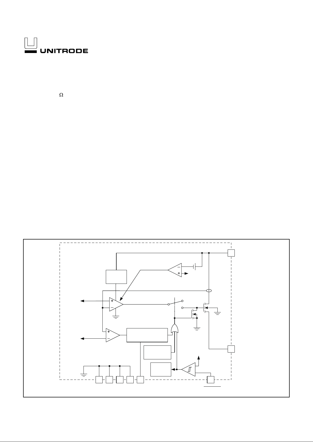
The current trip level is internally set at 1.65A, and the maximum current
level is also internally programmed for 2A. While the output current is below
the trip level of 1.65A, the internal power MOSFET is switched on at a nom
inal 220mΩ. When the output current exceeds the trip level but remains
less than the maximum current level, the MOSFET remains switched on,
but the fault timer starts charging CT. Once the fault time is reached, the cir
cuit will shut off for a time which equates to a 3% duty cycle. Finally, when
the output current reaches the maximum current level, the MOSFET transi
tions from a switch to a constant current source.
The UCC3916 is designed for uni-directional current flow, emulating a diode
in series with the power MOSFET.
The UCC3916 can be put in a sleep mode, drawing only 1µA of supply current.
Other features include thermal shutdown and low thermal resistance Small
Outline Power package.
SCSI Termpower Manager
8 OUTPUT
+
OUTPUT
CURRENT SENSE
H=OPEN
REVERSE VOLTAGE
COMPARATOR
50mV
CHARGE
PUMP
POWER
FET
ON TIME CONTROL
3% DUTY CYCLE
LINEAR
CURRENT
AMPLIFIER
THERMAL
SHUTDOWN
INTERNAL
BIAS
+
–
1.5V
5
SHTDWN
4
CT
OVER CURRENT
COMPARATOR
2 3 6 7
GNDGNDGNDGND
MAXIMUM
CURRENT
LEVEL
2A
4 HEATSINK PINS
CURRENT
TRIP LEVEL
1.65A
1
VIN
4V TO 6V
BLOCK DIAGRAM
UDG-99172
2
UCC3916
ABSOLUTE MAXIMUM RATINGS
VIN . . . . . . . . . . . . . . . . . . . . . . . . . . . . . . . . . . . . . . . . . . . +6V
Output Current
DC. . . . . . . . . . . . . . . . . . . . . . . . . . . . . . . . . . . Self Limiting
Pulse (Less than 100ns). . . . . . . . . . . . . . . . . . . . . . . . . 20A
Storage Temperature . . . . . . . . . . . . . . . . . . . –65°C to +150°C
Junction Temperature. . . . . . . . . . . . . . . . . . . –55°C to +150°C
Lead Temperature (Soldering, 10 sec.). . . . . . . . . . . . . +300°C
Currents are positive into, negative out of the specified termi
-
nal. Consult Packaging Section of Databook for thermal limita
-
tions and considerations of packages.
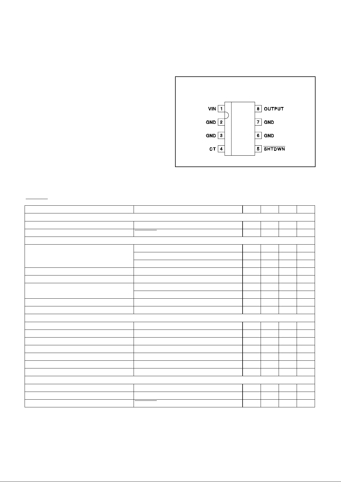
CONNECTION DIAGRAM
SOIC-8 (Top View)
DP Package
ELECTRICAL CHARACTERISTICS: Unless otherwise stated, these parameters apply for TJ = 0°C to +70°C; VIN = 5V,
SHTDWN
= 2.4V, TA =TJ.
PARAMETER TEST CONDITIONS MIN TYP MAX UNITS
Supply Current Section
ICC 1.00 2.00 mA
ICC - Sleep Mode SHTDWN
= 0.2V 0.50 5 µA
Output Section
Voltage Drop I
OUT = 1A 0.22 0.33 V
I
OUT = 1.5A 0.33 0.50 V
I
OUT = 1.65A 0.40 0.60 V
Trip Current –1.8 –1.65 –1.5 A
Max Current –2.4 –2 –1.65 A
Reverse Leakage VIN = 4.5V, V
OUT = 5V 6 20 µA
VIN = 0V, V
OUT = 5V 0.50 9 µA
Soft Start Time Initial Startup 50 µs
Short Circuit Response 100 ns
Fault Section
CT Charge Current V
CT = 1.0V –45 –36.0 –27 µA
CT Discharge Current V
CT = 1.0V 0.90 1.0 1.50 µA
Output Duty Cycle V
OUT = 0V 2.00 3.00 6.00 %
CT Charge Threshold 0.4 0.5 0.6 V
CT Discharge Threshold 1.2 1.4 1.8 V
Thermal Shutdown 170 °C
Thermal Hysteresis 10 °C
Shutdown Section
Shutdown Threshold 1.5 3.0 V
Shutdown Hysteresis 150 300 mV
Shutdown Bias Current SHTDWN
= 1.0V 100 500 nA
Note 1: All voltages are with respect to ground.

3
UCC3916
PIN DESCRIPTIONS
CT:A capacitor is applied between this pin and ground to
set the maximum fault time. The maximum fault time
must be more than the time to charge external capaci
-
tance. The maximum fault time is defined as:
T
FAULT= 28 • 10
3
• CT.
Once the fault time is reached the output will shutdown
for a time given by:
T
SD = 1 • 10
6
• CT
this results in a 3% duty cycle. 0.1µF is recommended
for SCSI applications to achieve the normal maximum
capacitance on the Termpwr line.
SHTDWN
: The IC enters a low-power sleep mode when
this pin is low and exits the sleep mode when this pin is
high.
VIN: Input voltage to the circuit breaker, ranging from 4V
to 6V.
VOUT: Output voltage of the circuit breaker. When
switched, the output voltage is approximately:
V
OUT = VIN – (220mΩ) • IOUT.
UNITRODE CORPORATION
7 CONTINENTAL BLVD.• MERRIMACK, NH 03054
TEL. (603) 424-2410 FAX (603) 424-3460
5
1
8
4
2 3 6 7
UCC3916VIN
SHTDWN
GND GND GND GND
CT
OUTPUT
C
T
C
LOAD
C
IN
V
IN
TERMPOWER
BUS
D1
TYPICAL APPLICATION
UDG-99169
Protecting The UCC3916 From Voltage Transients
The parasitic inductance associated with the power dis
-
tribution can cause a voltage spike at V
IN
if the load cur
-
rent is suddenly interrupted by the UCC3916.
It is
important to limit the peak of this spike to less than 6V to
prevent damage to the UCC3916
. This voltage spike can
be minimized by:
•
Reducing the power distribution inductance (e.g., twist
the positive (+) and negative (–) leads of the power
supply feeding V
IN
pin, locate the power supply close
to the UCC3916 or use a PCB ground plane).
•
Decoupling V
IN
with a capacitor, CIN, located close to
the V
IN
. This capacitor is typically less than 1µF to limit
the inrush current.
•
Clamping the voltage at V
IN
below 6V with a Zener
diode, D1, located close to the V
IN
pin.
SAFETY RECOMMENDATIONS
Although the UCC3916 is designed to provide system
protection for all fault conditions, all integrated circuits
can ultimately fail short. For this reason, if the UCC3916
is intended for use in safety critical applications where
UL
©
or some other safety rating is required, a redundant
safety device such as a fuse should be placed in series
with the device. The UCC3916 will prevent the fuse from
blowing virtually all fault conditions, increasing system
reliability and reducing maintainence cost, in addition to
providing the hot swap benefits of the device.
APPLICATION INFORMATION
 Loading...