

Datasheet UCC3837N, UCC3837DTR, UCC3837D, UCC2837N, UCC2837DTR Datasheet (Texas Instruments)
...
UCC1837
UCC2837
UCC3837
SLUS228A - AUGUST 1999
FEATURES
•
On Board Charge Pump to Drive
External N-MOSFET
•
Input Voltage as Low as 3V
•
Duty Ratio Mode Over Current
Protection
•
Extremely Low Dropout Voltage
•
Low External Parts Count
•
Output Voltages as Low as 1.5V
8-Pin N-FET Linear Regulator Controller
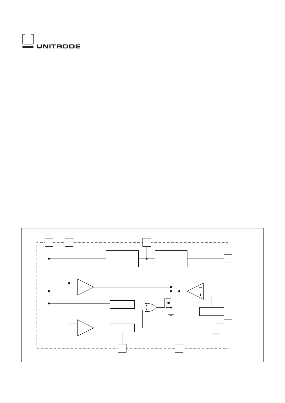
1
5
28
6
3
47
CHARGE
PUMP
CAP
LEVEL
SHIFT
1.5V REF
UVLO
TIMER
CURRENT SENSE
COMPARATOR
COMPCT
CSVDD
CURRENT SENSE
AMPLIFIER
++
VOUT
FB
GND100mV
140mV
ERROR AMPLIFIER
BLOCK DIAGRAM
UDG-99145
DESCRIPTION
The UCC3837 Linear Regulator Controller includes all the features re
quired for an extremely low dropout linear regulator that uses an external
N-channel MOSFET as the pass transistor. The device can operate from
input voltages as low as 3V and can provide high current levels, thus pro
viding an efficient linear solution for custom processor voltages, bus ter
mination voltages, and other logic level voltages below 3V. The on board
charge pump creates a gate drive voltage capable of driving an external
N-MOSFET which is optimal for low dropout voltage and high efficiency.
The wide versatility of this IC allows the user to optimize the setting of
both current limit and output voltage for applications beyond or between
standard 3-terminal linear regulator ranges.
This 8-pin controller IC features a duty ratio current limiting technique that
provides peak transient loading capability while limiting the average
power dissipation of the pass transistor during fault conditions. See the
Application Section for detailed information.
2
UCC1837
UCC2837
UCC3837
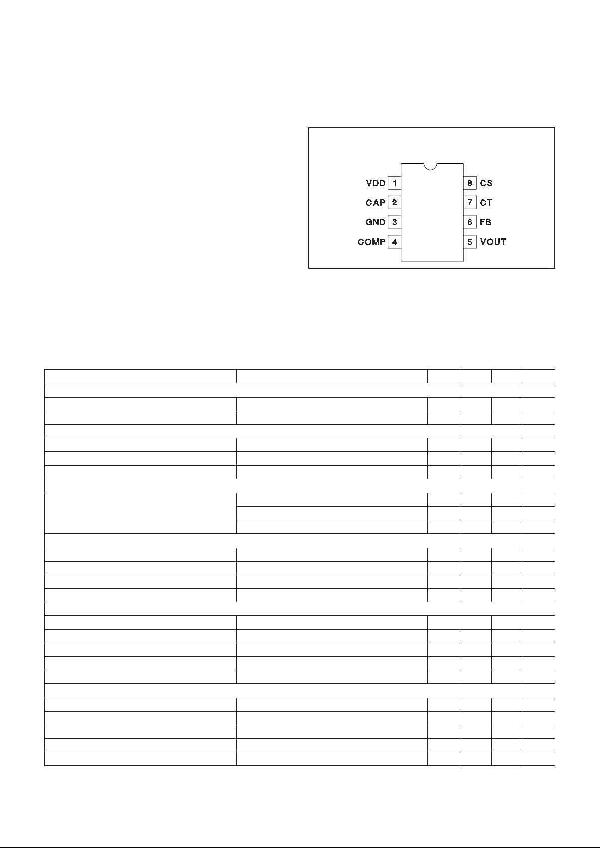
CONNECTION DIAGRAM
ELECTRICAL CHARACTERISTICS:
Unless otherwise specified, TA= –55°C to 125°C for the UCC1837, –25°C to 85°C
for the UCC2837 and 0°C to 70°C for UCC3837; VDD = 5V, CT= 10nF, C
CAP
= 100nF.
PARAMETER TEST CONDITIONS MIN TYP MAX UNITS
Input Supply
Supply Current VDD = 5V 1 1.5 mA
VDD = 10V 1.2 2 mA
Under Voltage Lockout
Minimum Voltage to Start 2.00 2.65 3.00 V
Minimum Voltage After Start 1.6 2.2 2.6 V
Hysteresis 0.25 0.45 0.65 V
Reference ( Note 1 )
V
REF 25°C 1.485 1.5 1.515 V
0°C to 70°C 1.470 1.5 1.530 V
–55°C to 125°C 1.455 1.5 1.545 V
Current Sense
Comparator Offset 0°C to 70°C 90 100 110 mV
Comparator Offset –55°C to 125°C 85 100 115 mV
Amplifier Offset 120 140 160 mV
Input Bias Current V
CS = 5V 0.5 5 µA
Current Fault Timer
CT Charge Current V
CT = 1V 16 36 56 µA
CT Discharge Current V
CT = 1V 0.4 1.2 1.9 µA
CT Fault Low Threshold 0.4 0.5 0.6 V
CT Fault Hi Threshold 1.3 1.5 1.7 V
Fault Duty Cycle 2 3.3 5 %
Error Amplifier
Input Bias Current 0.5 2 µA
Open Loop Gain 60 90 dB
Transconductance –10µA to 10µA 2 5 8 mMho
Charge Current V
COMP = 6V 20 40 60 µA
Discharge Current V
COMP = 6V 10 25 40 µA
DIL-8, SOIC-8 (Top View)
J or N Package, D Package
ABSOLUTE MAXIMUM RATINGS
All pins referenced to GND . . . . . . . . . . . . . . . . .–0.3V to +15V
CS, CT, FB. . . . . . . . . . . . . . . . . . . . . . . . –0.3V to VDD + 0.3V
Storage Temperature . . . . . . . . . . . . . . . . . . . –65°C to +150°C
Junction Temperature. . . . . . . . . . . . . . . . . . . –55°C to +150°C
Lead Temperature (Soldering, 10sec.) . . . . . . . . . . . . . +300°C
Currents are positive into, negative out of the specified terminal.
Consult Packaging Section of Databook for thermal limitations
and considerations of packages.

3
UCC1837
UCC2837
UCC3837
ELECTRICAL CHARACTERISTICS:
Unless otherwise specified, TA= –55°C to 125°C for the UCC1837, –25°C to 85°C
for the UCC2837 and 0°C to 70°C for UCC3837; VDD = 5V, CT= 10nF, C
CAP
= 100nF.
PARAMETER TEST CONDITIONS MIN TYP MAX UNITS
FET Driver
Peak Output Current V
CAP = 10V, VOUT = 1V 0.5 1.5 2.5 mA
Average Output Current VOUT = 1V 25 100 175 µA
Max Output Voltage VDD = 4.5V, I
OUT = 0µA 8.4 9.7 V
VDD = 4.5V, I
OUT = 10µA, 0°C to 70°C 8 9 V
VDD = 4.5V, I
OUT = 10µA, –55°C to 125°C 7.5 9 V
Charge Pump
CAP Voltage VDD = 4.5V, C/S = 0V 11 12.5 V
VDD = 12V, C/S = 0V 15 16.5 V
Note 1: This is defined as the voltage on FB which results in a DC voltage of 8V on VOUT.
PIN DESCRIPTIONS
CAP: The output of the charge pump circuit. A capacitor
is connected between this pin and GND to provide a
floating bias voltage for an N-Channel MOSFET gate
drive. A minimum of a 0.01µF ceramic capacitor is rec-
ommended. CAP can be directly connected to an external regulated source such as +12V, in which case the
external voltage will be the source for driving the
N-Channel MOSFET.
COMP: The output of the transconductance error amplifier and current sense amplifier. Used for compensating
the small signal characteristics of the voltage loop (and
current loop when Current Sense Amplifier is active in
over curret mode).
CS: The negative current sense input signal. This pin
should be connected through a low noise path to the low
side of the current sense resistor.
CT: The input to the duty cycle timer circuit. A capacitor
is connected from this pin to GND, setting the maximum
ON time of the over current protection circuits. See the
Application Section for programming instructions.
FB: The inverting terminal of the voltage error amplifier,
used to feedback the output voltage for comparison with
the internal reference voltage. The nominal DC operating
voltage at this pin is 1.5V
GND: Ground reference for the device. For accurate output voltage regulation, GND should be referenced to the
output load ground.
VDD: The system input voltage is connected to this
point. VDD must be above 3V. VDD also acts as one
side of the Current Sense Amplifier and Comparator.
VOUT: This pin directly drives the gate of the external
N-MOSFET pass element. The typical output impedance
of this pin is 6.5kΩ.
Topology and General Operation
Unitrode Application Note U-152 is a detailed design of a
low dropout linear regulator using an N-channel
MOSFET as a pass element, and should be used as a
guide for understanding the operation of the circuit
shown in Fig. 1.
Charge Pump Operation
The internal charge pump of the UCC3837 is designed to
create a voltage equal to 3 times the input VDD voltage
at the CAP pin. There is an internal 5V clamp at the input
of the charge pump however that insures the voltage at
CAP does not exceed the ratings of the IC. This CAP
voltage is used to provide gate drive current to the exter
-
nal pass element as well as bias current to internal sec
-
tions of the UCC3837 itself. The charge pump output has
a typical impedance of 80kΩ and therefore the loading of
the IC and the external gate drive reduces the voltage
from its ideal level. The UCC3837 can operate in several
states including having the error amplifier disabled (shut
down), in normal linear regulation mode, and in overdrive
mode where the linear regulator is responding to a tran
sient load or line condition. The maximum output voltage
available at VOUT is shown in Fig. 2 for these various
modes of operation.
The charge pump output is designed to supply 10µAof
average current to the load which is typically the
MOSFET gate capacitance present at the VOUT pin.The
capacitor value used at CAP is chosen to provide holdup
APPLICATION INFORMATION

4
UCC1837
UCC2837
UCC3837
of the CAP voltage should the external load exceed the
average current, which occurs during load and line transient conditions. The value of CAP also determines the
startup time of the linear regulator. The voltage at CAP
charges up with a time constant determined by the
charge pump output impedance (typically 80kΩ) and the
value of the capacitor on CAP.
An external voltage such as +12V may be tied to the
CAP pin directly to insure a higher value of VOUT, which
may be useful when a standard level MOSFET is used or
when VDD is very low and the resulting VOUT voltage
may need to be higher. With an external source applied
to CAP, the maximum voltage at VOUT will be approxi
mately 1V below the external source.The external +12V
source should be decoupled to GND using a minimum of
a 0.01µF capacitor.
Choosing a Pass Element
The UCC3837 is designed for use with an N-channel
MOSFET pass element only. The designer may choose
a logic level or standard gate level MOSFET depending
on the input voltage, the required gate drive, and the
available voltage at VOUT as discussed previously.
MOSFET selection should be based on required dropout
voltage and gate drive characteristics. A lower R
DS(on)
MOSFET is used when low dropout is required, but this
type of MOSFET will have higher gate capacitance which
may result in a slower transient response.
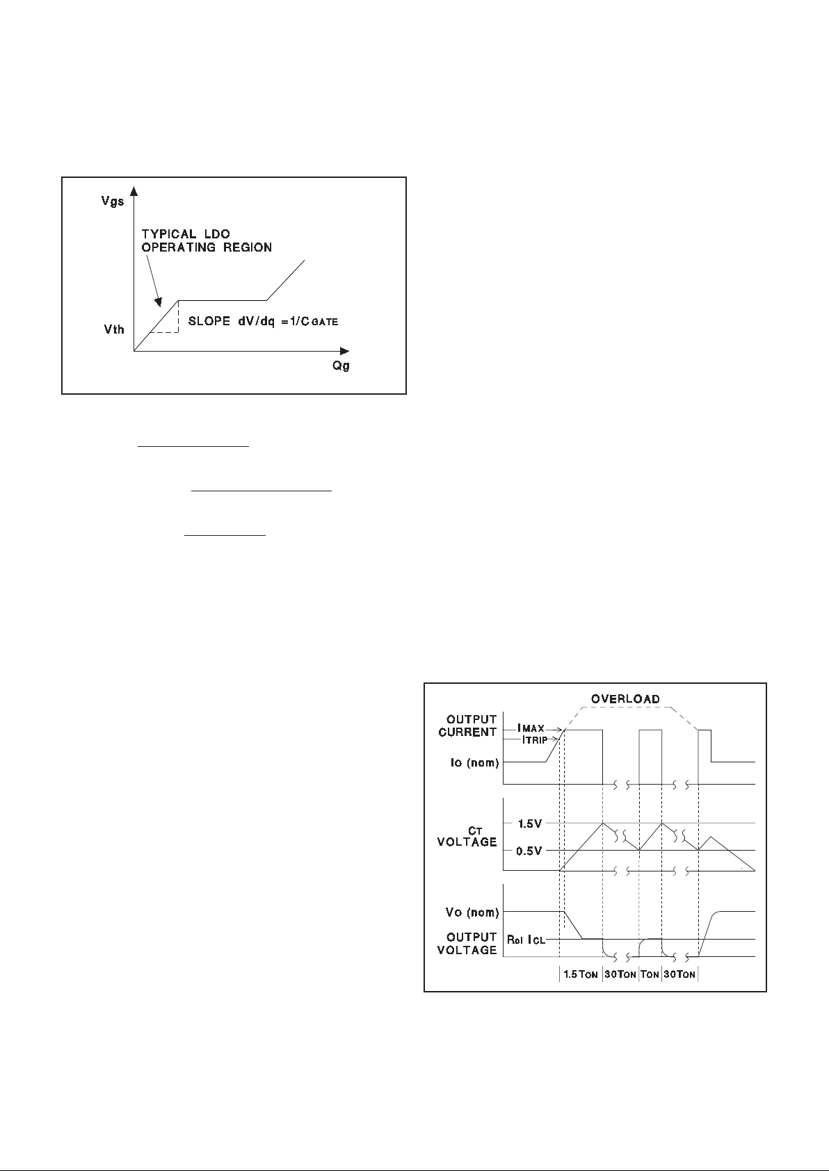
A MOSFET used in linear regulation is typically operated
at a gate voltage between the threshold voltage and the
gate plateau voltage in order to maintain high gain. This
mode of operation is linear, and therefore the channel resistance is higher than the manufacturer’s published
R
DS(on)
value. The MOSFET should only be operated in
the non-linear (switch) mode under transient conditions,
when minimum dropout voltage is required.
Disabling the UCC3837
Grounding the CAP pin will remove the drive voltage and
effectively disable the output voltage. The device used to
short the output of CAP should have a very low leakage
current when in the OPEN state, since even a few
microamps will lower the charge pump voltage.
A second method of disabling the UCC3837 is to place a
short circuit across C
COMP
. This will have an advantage
of a quicker restart time as the voltage at CAP will not be
completely discharged. The charge pump will be loaded
down by the typical 40µA charging current of the error
amplifier with this configuration, resulting in a lower volt
-
age at CAP.
Compensating the Error Amplifier
Using a MOSFET as an external pass element intro
duces a pole in the control loop that is a function of the
UCC3837 output impedance, R
OUT
, typically 6.5kΩ, and
the MOSFET input gate capacitance. Fig. 3 indicates
that in the normal operation of a linear regulator using a
MOSFET, the gate capacitance can be predicted directly
from the MOSFET characteristic charge curve, using the
relationship:
C
Qgth
Vgth
IN
=
∆
∆
This pole can be canceled by programming a zero fre
quency on the output of the UCC3837 error amplifier
equal to the pole frequency. Therefore:
8
1VDD
CS
5VOUT
2CAP
7CT
4COMP
6FB
3GND
Q1
IRL2203N
OR EQUIVALENT
R2
1.8k
R3
1.5k
C3
1000µF
3.3V
R1
0.020
R
COMP
10k
C
COMP
820pF
0.1µF
0.1µFQ1
C1
330µF
5V
ON/OFF
UCC3837
Figure 1. Typical application 5V to 3.3V, 5A
APPLICATION INFORMATION
5
6
7
8
9
10
11
12
13
14
15
3456789101112
VDD
VOUT
E/A DISABLED
LINEAR REGULATOR
OVERDRIVE
Figure 2. Typical V
OUT(max)
vs. VDD.
UDG-99137
5
UCC1837
UCC2837
UCC3837
F
CR
POLE
IN OUT
=
•• •
1
2
π
FF
RC
ZERO POLE
COMP COMP
==
•• •
1
2 π
RC
F
COMP COMP
POLE
=
••
1
2 π
where CINis the MOSFET input capacitance and R
OUT
is
the output impedance of VOUT.
The value of C
COMP
should be large enough that
parasitics connected to COMP do not effect the zero frequency. A minimum of 220pF is recommended.
Transient Response
The transient performance of a linear regulator built using the UCC3837 can be predicted by understanding the
dynamics of the transient event. Consider a load tran
sient on the application circuit of Fig. 1, where the output
current steps from a low value to a high value. Initially,
the output voltage will drop as a function of the output
capacitors ESR times the load current change. In re
sponse to the decrease in feedback voltage at FB, the
UCC3837 error amplifier will increase its charge current
to a typical value of 40µA. The output of the amplifier will
therefore respond by first stepping the voltage propor
tional to 40µA times R
COMP
, and then ramping up pro
portional to 40µA and the value of C
COMP
. Dynamic
response can therefore be improved by increasing
R
COMP
and decreasing C
COMP
.
The value of VOUT will increase the same amount as the
increase in the error amplifier output. The UCC3837 out
-
put gate drive current, however, is internally limited to
1.5mA. The response of the voltage at the gate of the ex
ternal pass element is therefore a function of the 1.5mA
drive current and the external gate charge, as obtained
from the MOSFET data sheet gate charge curve.
For the application circuit shown in Fig. 1, the voltage at
the error amplifier output will increase quickly by 400mV
due to the 40µA current through R
COMP
. The error am
-
plifier will then slew at approximately 50mV per micro
-
second as the 40µA charges C
COMP
.
From the IRL2203N data sheet, the typical required gate
voltage at room temperature, to deliver 5A is 2.6V. The
threshold for the device is approximately 1.5V. From the
gate charge curve for the IRL2203N, approximately 7nC
charge is required to change the gate voltage from 1.5V
to 2.6V. With 1.5mA gate drive current, the required time
to charge the gate is therefore 4.7µs.
Overcurrent Protection and Thermal Management:
Overcurrent protection is provided via the UCC3837’s in
ternal current amplifier and overcurrent comparator. If at
any time the voltage across the current sense resistor
crosses the comparator threshold, the UCC3837 begins
to modulate the output driver at a 3% duty cycle. During
the 3% on time, if the current forces 140mV across the
sense amplifier, the UCC3837 will enter a constant output current mode. Fig. 4 illustrates the cyclical retry of
the UCC3837 under fault conditions. Note that the initial
fault time is longer than subsequent cycles due to the
fact that the timing capacitor is completely discharged
and must initially charge to the reset threshold of 0.5V.
Figure 3. MOSFET turn-on characteristics.
APPLICATION INFORMATION (cont.)
UDG-97046
Figure 4. Load current, timing capacitor voltage and
output voltage under fault conditions.
UDG-97046

6
UCC1837
UCC2837
UCC3837
Fault time duration is controlled by the value of the timing
capacitor, CT, according to the following equation:
tC
V
I
CC
FAULT T T T
=• =•
−
•
=••
−
∆
15 0 5
36 10
278 10
6
3
..
.
(1)
Fig. 5 provides a plot of fault time vs. timing capacitance.
The fault time duration is set based upon the load capac
itance, load current, and the maximum output current.
The “on” or fault time must be of sufficient duration to
charge the load capacitance during a normal startup se
quence or when recovering from a fault. If not, the
charge accumulated on the output capacitance will be
depleted by the load during the “off” time. The cycle will
then repeat, preventing the output from turning on.
To determine the minimum fault time, assume a maxi
mum load current just less than the trip limit. This leaves
the difference between the IMAX and I
TRIP
values as the
current available to charge the output capacitance. The
minimum required fault time can then be calculated as
follows:
()
t
CV
II
FAULT
OUT OUT
MAX TRIP
min
=
•
−
(2)
The minimum timing capacitor can be calculated by sub
-
stituting equation (1) for t
FAULT
in equation (2) and solv
-
ing for CT.
()
()
C
CV
II
T
OUT OUT
MAX TRIP
min
.
=
•
•• −27 8 10
3
(3)
Switchmode protection offers significant heat sinking ad
-
vantages when compared to conventional, constant cur
rent solutions. Since the average power during a fault
condition is reduced as a function of the duty cycle, the
heat sink need only have adequate thermal mass to ab
sorb the maximum steady state power dissipation and
not the full short circuit power. With a 5.25V input and a
maximum output current of 5A, the power dissipated in
the MOSFET is given by:
()
PV V V I
IN SENSE OUT OUT
=− − •
(4)
()
()
PW
=−•−•=5255002335925....
Given that the thermal resistivity of the MOSFET is spec
ified as 1°C/W for the TO-220 package style and assum
ing an ambient temperature of 50°C and a case to heat
sink resistivity of θ
CS
= 0.3°C/W, the heat sink required
to maintain a 125°C junction temperature can be calcu
lated as follows:
()
TTP
J
A
JC CS SA
=+ + +θθθ
(5)
()
125 50 9 25 1 03=+ •++..θ
SA
θ
SA
C
W
≤°68.
Based on this analysis, any heatsink with a thermal resistivity of 6.8 °C/W or less should suffice. The current in
the circuit of Fig. 1, under short circuit conditions, will be
limited to 7A at a 3% duty cycle, resulting in a MOSFET
power dissipation of only:
()
()
()[]
PV I R I Duty
IN OUT SENSE OUT
=−•••
max
(6)
()
()[]
PW
=−• ••=5257 002 7 003107.. ..
Without switchmode protection, the short circuit power
dissipation would be 35.8W, almost four times the nomi
nal dissipation.
Using Printed Circuit Board Etch as a Sense Resistor
Unitrode Design Note DN-71 discusses the use of
printed circuit board copper etch as a low ohm sense re
sistor. This technique can easily be applied when using
the UCC3837. The application circuit shown in Fig. 1 can
be used as an example. This linear regulator is designed
with a 5A average load current, demanding a 20mΩ
sense resistor to result in a 100mV current sense com
parator signal for the UCC3837. The maximum ambient
temperature of the linear regulator is 70°C.
Using DN-71, a 1 ounce outer layer etch of 0.05 inches
wide and 1.57 inches long results in a resistance of
20mΩ at an ambient temperature of 70°C and an operat
ing current of 5A. Because the resistivity of copper is a
function of temperature, the current limit at lower temper
atures will be higher, as shown in Fig. 6.
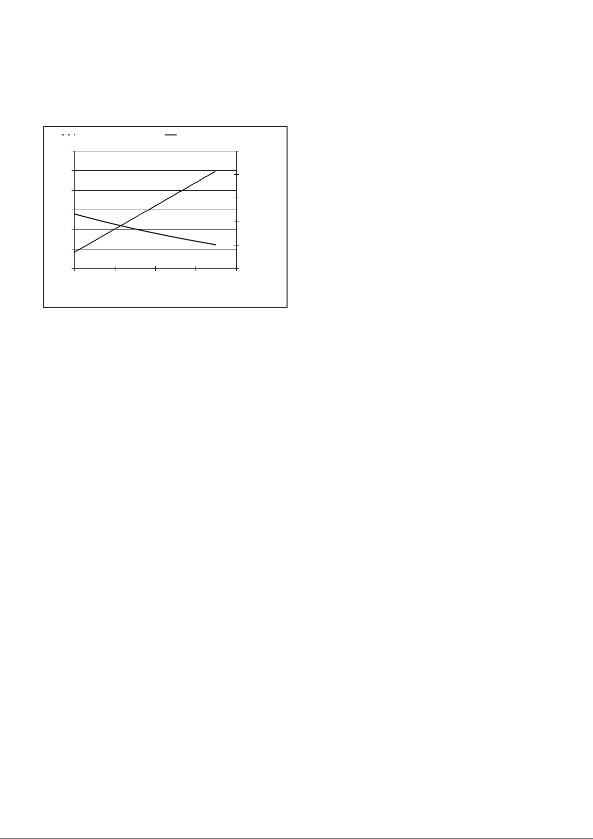
0
5
10
15
20
25
30
0 0.2 0.4 0.6 0.8 1
CT (uF)
FAULT TIME (ms)
Figure 5. Fault time vs. timing capacitance.
7
UCC1837
UCC2837
UCC3837
Practical Considerations
In order to achieve the expected performance, careful attention must be paid to circuit layout. The printed circuit
board should be designed using a single point ground,
referenced to the return of the output capacitor. All
traces carrying high current should be made as short and
wide as possible in order to minimize parasitic resistance
and inductance effects.
To illustrate the importance of these concepts, consider
the effects of a 1.5" PCB trace located between the out
put capacitor and the UCC3837 feedback reference. A
0.07" wide trace of 1oz. copper results in an equivalent
resistance of 10.4mΩ. At a load current of 3A, 31.2mV is
dropped across the trace, contributing almost 1% error to
the DC regulation. Likewise, the inductance of the trace
is approximately 3.24nH, resulting in a 91mV spike dur
ing the 100ns it takes the load current to slew from
200mA to 3A.
The dropout voltage of a linear regulator is often a key
design parameter. Calculations of the dropout voltage of
a linear regulator based on the UCC3837 Controller
should consider all of the following:
•
Sense resistor drop, including temperature and
tolerance effects,
• Path resistance drops on both the input and output
voltages,
• MOSFET resistance as a function of temperature and
gate drive, including transient performance,
• Ground path drops.
APPLICATION INFORMATION
15
16
17
18
19
20
21
0 20406080
AMBIENT TEMPERATURE [°C]
4
5
6
7
8
9
RESISTANCE SHORT CIRCUIT LIMIT
COPPER RESISTANCE [mW]
SHORT CIRCUIT CURRENT
Figure 6. Copper resistance and short circuit limit
for example resistor.
UNITRODE CORPORATION
7 CONTINENTAL BLVD. • MERRIMACK, NH 03054
TEL. (603) 424-2410 FAX (603) 424-3460

IMPORTANT NOTICE
T exas Instruments and its subsidiaries (TI) reserve the right to make changes to their products or to discontinue
any product or service without notice, and advise customers to obtain the latest version of relevant information
to verify, before placing orders, that information being relied on is current and complete. All products are sold
subject to the terms and conditions of sale supplied at the time of order acknowledgement, including those
pertaining to warranty, patent infringement, and limitation of liability.
TI warrants performance of its semiconductor products to the specifications applicable at the time of sale in
accordance with TI’s standard warranty. Testing and other quality control techniques are utilized to the extent
TI deems necessary to support this warranty. Specific testing of all parameters of each device is not necessarily
performed, except those mandated by government requirements.
CERT AIN APPLICATIONS USING SEMICONDUCTOR PRODUCTS MAY INVOLVE POTENTIAL RISKS OF
DEATH, PERSONAL INJURY, OR SEVERE PROPERTY OR ENVIRONMENTAL DAMAGE (“CRITICAL
APPLICATIONS”). TI SEMICONDUCTOR PRODUCTS ARE NOT DESIGNED, AUTHORIZED, OR
WARRANTED TO BE SUITABLE FOR USE IN LIFE-SUPPORT DEVICES OR SYSTEMS OR OTHER
CRITICAL APPLICATIONS. INCLUSION OF TI PRODUCTS IN SUCH APPLICA TIONS IS UNDERSTOOD T O
BE FULLY AT THE CUSTOMER’S RISK.
In order to minimize risks associated with the customer’s applications, adequate design and operating
safeguards must be provided by the customer to minimize inherent or procedural hazards.
TI assumes no liability for applications assistance or customer product design. TI does not warrant or represent
that any license, either express or implied, is granted under any patent right, copyright, mask work right, or other
intellectual property right of TI covering or relating to any combination, machine, or process in which such
semiconductor products or services might be or are used. TI’s publication of information regarding any third
party’s products or services does not constitute TI’s approval, warranty or endorsement thereof.
Copyright 1999, Texas Instruments Incorporated
 Loading...