

Datasheet UCC381DPTR-ADJ, UCC381DPTR-5, UCC381DP-ADJ, UCC381DP-5, UCC381DP-3 Datasheet (Texas Instruments)
...
Low Dropout 1 Ampere Linear Regulator Family
UCC281-3/-5/-ADJ
UCC381-3/-5/-ADJ
FEATURES
Precision Positive Linear Voltage
•
Regulation
0.5V Dropout at 1A
•
Guaranteed Reverse Input/ Output
•
Voltage Isolation with Low Leakage
Low Quiescent Current Irrespective of
•
Load
Adjustable Output Voltage Version
•
Fixed Versions for 3.3V and 5V
•
Outputs
Logic Shutdown Capability
•
Short Circuit Power Limit of
•
3% • V
• Remote Load Voltage for Accurate
Load Regulation
• Current Limit
IN
DESCRIPTION
The UCC381-3/-5/-ADJ family of positive linear series pass regulators is
tailored for low drop out applications where low quiescent power is impor
tant. Fabricated with a BiCMOS technology ideally suited for low input to
output differential applications, the UCC381 will pass 1A while requiring
only 0.5V of input voltage headroom. Dropout voltage decreases linearly
with output current, so that dropout at 200mA is less than 100mV. Quies
cent current is always less than 650µA. To prevent reverse current conduc
tion, on-chip circuitry limits the minimum forward voltage to typically 50mV.
Once the forward voltage limit is reached, the input-output differential volt
age is maintained as the input voltage drops until undervoltage lockout dis
ables the regulator.
UCC381-3 and UCC381-5 versions have on-chip resistor networks preset
to regulate either 3.3V or 5.0V, respectively. Furthermore, remote sensing
of the load voltage is possible by connecting the VOUTS pin directly at the
load. The output voltage is then regulated to 1.5% at room temperature and
better than 2.5% over temperature. The UCC381-ADJ version has a regu
lated output voltage programmed by an external user-definable resistor ratio.
(continued)
-
-
-
-
-
-
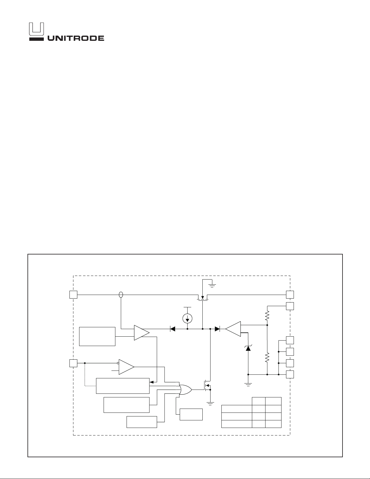
BLOCK DIAGRAM
8
VIN
SHUTDOWN FOR FIXED VERSIONS
5
CT*
*ADJ
VERSION
ONLY
1.3/2.1A
CURRENT
REFERENCE
0.65V
3% DUTY CYCLE
CURRENT LIMIT TIMER
REVERSE VOLTAGE
SENSE
CURRENT
LIMIT
–
+
THERMAL
SHUTDOWN
V
PUMP
UVLO
VOLTAGE
AMPLIFIER
–
+
UCC381-ADJ
UCC381-3
UCC381-5
R2
1.25V
R1
R2 R1
0 OPEN
82k 50k
150k 50k
1VOUT
VOUTS
4
2GND
3GND
6
GND
GND
7
SLUS214A - NOVEMBER 1999
UDG-98112
UCC281-3/-5/-ADJ
UCC381-3/-5/-ADJ
ABSOLUTE MAXIMUM RATINGS
VIN. . . . . . . . . . . . . . . . . . . . . . . . . . . . . . . . . . . . . . . . . . . . . 9V
CT . . . . . . . . . . . . . . . . . . . . . . . . . . . . . . . . . . . . . . . −0.3 to 3V
Storage Temperature . . . . . . . . . . . . . . . . . . . −65°C to +150°C
Junction Temperature. . . . . . . . . . . . . . . . . . . −55°C to +150°C
Lead Temperature (Soldering, 10 sec.) . . . . . . . . . . . . . +300°C
Currents are positive into, negative out of the specified terminal.
Consult Packaging Section of Databook for thermal limitations
and considerations of packages. All voltages are referenced to
GND.
DESCRIPTION (cont.)
Short circuit current is internally limited. The device re
sponds to a sustained overcurrent condition by turning
off after a T
riod, T
OFF
then begins pulsing on and off at the T
duty cycle of 3%. This drastically reduces the power dissipation during short circuit such that heat sinking, if at all
required, must only accommodate normal operation. On
the fixed output versions of the device T
400µs − a guaranteed minimum. On the adjustable version an external capacitor sets the on time. The off time
is always 32 times T
delay. The device then stays off for a pe
ON
, that is 32 times the TONdelay. The device
/(TON+T
ON
ON
ON is fixed at
.
OFF
CONNECTION DIAGRAMS
SOIC-8 (Top View)
DP Package
VOUT
VOUTS
GND
GND
1
2
3
4
* ADJ version only
-
The UCC381 can be shutdown to 25µA (max) by pulling
the CT pin low.
Internal power dissipation is further controlled with ther
mal overload protection circuitry. Thermal shutdown oc
)
curs if the junction temperature exceeds 165°C. The chip
will remain off until the temperature has dropped 20°C.
The UCC281 series is specified for operation over the industrial range of −40°Cto+85°C, and the UCC381 se-
ries is specified from 0°Cto+70°C. These devices are
available in the 8 pin DP surface mount power package.
For other packaging options consult the factory.
VIN
8
GND
7
GND
6
CT*
5
-
-
ELECTRICAL CHARACTERISTICS: Unless otherwise stated, these specifications hold for TA = 0°C to 70°C for the
UCC381-X series and −40°C to +85°C for the UCC283-X series, V
the UCC381-ADJ version and V
set to 5V. TJ= TA.
OUT
IN=VOUT
PARAMETER TEST CONDITIONS MIN TYP MAX UNITS
UCC381-5 Fixed 5V, 1A Family
Output Voltage T
= 25°C 4.925 5 5.075 V
J
Over Temperature 4.875 5.125 V
Line Regulation V
Load Regulation I
Drop Out Voltage, V
IN–VOUT
Peak Current Limit V
= 5.15V to 9V 1 3 mV
IN
= 0mA to 1A 2 5 mV
OUT
I
= 1A, V
OUT
= 200mA, V
I
OUT
= 0V 2 3.5 A
OUT
= 4.85V, TA < 85°C 0.5 0.6 V
OUT
OUT
Overcurrent Threshold 1 1.8 A
Current Limit Duty Cycle V
Overcurrent Time Out, T
ON
= 0V 3 5 %
OUT
V
= 0V 400 750 1600 µs
OUT
Quiescent Current 400 650 µA
Quiescent Current in Shutdown V
Shutdown Threshold At C
Reverse Leakage Current 1V < V
UVLO Threshold V
= 9V 10 25 µA
IN
Input 0.25 0.65 V
T
IN<VOUT,VOUT
where V
IN
passes current 2.5 2.8 3.0 V
OUT
+ 1.5V, I
OUT
= 0mA, C
= 2.2µF. CT= 1500pF for
OUT
= 4.85V, TA < 85°C 100 200 mV
< 5.1V, at VOUT 75 µA
2
UCC281-3/-5/-ADJ
UCC381-3/-5/-ADJ
ELECTRICAL CHARACTERISTICS:
UCC381-X series and −40°C to +85°C for the UCC283-X series, V
the UCC381-ADJ version and V
set to 5V. TJ= TA.
OUT
Unless otherwise stated, these specifications hold for TA = 0°C to 70°C for the
IN=VOUT
+ 1.5V, I
OUT
= 0mA, C
= 2.2µF. CT= 1500pF for
OUT
PARAMETER TEST CONDITIONS MIN TYP MAX UNITS
UCC381-3 Fixed 3.3V, 1A Family
Output Voltage T
= 25°C 3.25 3.3 3.35 V
J
Over Temperature 3.22 3.38 V
Line Regulation V
Load Regulation I
Dropout Voltage, V
IN-VOUT
Peak Current Limit V
= 3.45V to 9V 1 3 mV
IN
= 0mA to 1A 2 5 mV
OUT
I
= 1A, V
OUT
= 200mA, V
I
OUT
= 0V 2 3.5 A
OUT
= 3.15V, TA < 85°C 0.6 0.8 V
OUT
= 3.15V, TA< 85°C 100 200 mV
OUT
Overcurrent Threshold 1 1.8 A
Current Limit Duty Cycle V
Overcurrent Time Out, T
ON
= 0V 3 5 %
OUT
V
= 0V 400 750 1600 µs
OUT
Quiescent Current 400 650 µA
Quiescent Current in Shutdown V
Shutdown Threshold At C
Reverse Leakage Current 1V < V
UVLO Threshold V
= 9V 10 25 µA
IN
Input 0.25 0.65 V
T
IN<VOUT,VOUT
where V
IN
OUT
< 3.35V, at VOUT 75 µA
passes current 2.5 2.8 3.0 V
UCC381-ADJ Adjustable Output, 1A Family
Regulating Voltage at ADJ Input T
= 25°C 1.23 1.25 1.27 V
J
Over Temperature 1.22 1.28 V
Line Regulation, at ADJ Input V
Load Regulation, at ADJ Input I
Dropout Voltage, V
IN-VOUT
Peak Current Limit V
IN=VOUT
OUT
I
OUT
I
OUT
OUT
+ 150mV to 9V 1 3 mV
= 0mA to 1A 2 5 mV
= 1A, V
= 200mA, V
= 4.85V 0.5 0.6 V
OUT
= 4.85V 100 200 mV
OUT
= 0V 2 3.5 A
Overcurrent Threshold 1 1.8 A
Current Limit Duty Cycle V
Overcurrent Time Out, T
ON
= 0V 3 5 %
OUT
V
= 0V, CT= 1500pF 400 1000 1600 µs
OUT
Quiescent Current 400 650 µA
Quiescent Current in Shutdown V
Shutdown Threshold At C
Reverse Leakage Current 1V < V
= 9V 10 25 µA
IN
Input 0.25 0.65 V
T
IN<VOUT,VOUT
< 9V, at V
OUT
100 µA
Bias Current at ADJ Input 100 250 nA
UVLO Threshold V
where V
IN
passes current 2.5 2.8 3.0 V
OUT
3

PIN DESCRIPTIONS
UCC281-3/-5/-ADJ
UCC381-3/-5/-ADJ
CT: For UCC381-3 and UCC381-5 versions, this is the
shutdown pin which, when pulled low, turns off the regu
lator output and puts the device in a low current state.
For the UCC381-ADJ version, a capacitor is required be
tween the CT pin and GND to set the T
time during
ON
overcurrent according to the following (typical) equation:
TC
=•660 000,
ON CT
GND: All voltages are measured with respect to this pin.
This is the low noise ground reference input for regula
tion. The output decoupling capacitor should be tied to
PIN 7.
VIN: Positive supply input for the regulator. Bypass this
pin to GND with at least 1µF of low ESR, ESL capaci
tance if the source is located further than 1 inch from the
device.
VOUT: Output for regulator. The regulator does not re
quire a minimum output capacitor for stability. Choose
the appropriate size capacitor for the application with re-
spect to the required transient loading. For example, if
the load is very dynamic, a large capacitor will smooth
out the response to load steps.
VOUTS: Feedback for regulator sensing of the output
voltage. For loads which are a considerable resistive dis
tance from the VOUT pin, the VOUTS pin can be used to
move the resistance into the control loop of the regulator,
thereby effectively canceling the IR drop associated with
the load path. For local regulation, merely connect this
pin directly to the VOUT pin. For the UCC381-ADJ ver
sion, the output voltage can be set by two external resi
tors according to the following relationship:
-
V
=•+
125 1
OUT
where R1 is a resistor connected between VOUT and
-
.
R
2
R
1
VOUTS and R2 is a resistor connected between VOUTS
and GND.
-
-
-
TYPICAL APPLICATION CIRCUIT
C
T
SHUTDOWN
5
CT
V
IN
8
VIN
1.0µF
GND GNDGNDGND
7 6 3 2
VOUTS
UCC381
VOUT
4
1
Note 1: R1 and R2 for adjustable version only. For 3.3V and 5V versions connect VOUT to VOUTS. See Pin Descriptions.
Note 2: C
timing capacitor is for adjustable version only. For 3.3V and 5V versions, the CT pin is used to enable or shutdown
T
the part. See Pin Descriptions.
NOTE 2
NOTE 1
C
OUT
R1
NOTE 1
R2
OUTPUT
UDG-98148
4

APPLICATION INFORMATION
Overview
The UCC381 family of low dropout linear (LDO) regula
tors provide a regulated output voltage for applications
with up to 1A of load current. The regulator features a
low dropout voltage and short circuit protection, making
their use ideal for demanding high current applications
requiring fault tolerance.
Short Circuit Protection
The UCC381 provides unique short circuit protection
circuitry that reduces power dissipation during a fault.
When an overload situation is detected, the device en
ters a pulsed mode of operation at 3% duty cycle re
ducing the heat sink requirements during a fault. The
UCC381 has two current thresholds that determine its
behavior during a fault as shown in Fig. 1.
When the regulator current exceeds the Overcurrent
Threshold for a period longer than the T
UCC381 shuts off for a period (T
T
. If the short circuit current exceeds the Peak Cur-
ON
) which is 32 times
OFF
rent Limit, the regulator limits the current to peak current limit during the T
period. The peak current limit
ON
is nominally 1 Amp greater than the overcurrent threshold. The regulator will continue in pulsed mode until the
fault is cleared as illustrated in Fig. 1.
ON
, the
UCC281-3/-5/-ADJ
UCC381-3/-5/-ADJ
A capacitive load on the regulator’s output will appear as a
short circuit during start-up. If the capacitance is too large,
the output voltage will not come into regulation during the
initial T
operation. The peak current limit, T
characteristics determine the maximum value of output ca
pacitor that can be charged. For a constant current load
the maximum output capacitance is given as follows:
CII
-
For worst case calculations the minimum values of on time
-
(T
ON
justable version allows the T
capacitor on the CT pin:
T C Farads
For a resistive load (R
can be estimated from:
period and the UCC381 will enter pulsed mode
ON
period, and load
ON
T
ON
=− •
OUT CL LOAD
()
()
max
V
Farads
OUT
) and peak current limit (ICL) should be used. The ad
time to be adjusted with a
ON
µµsec ,=•660 000
ON adj
C
Rn
() ( )
()
) the maximum output capacitor
LOAD
OUT
LOAD
=
max
()
l
•
T
ON
1
−
1
V
OUT
IR
•
CL LOAD
Farads
-
(1)
-
(2)
(3)
OUTPUT
CURRENT
I
(nom)
O
V
(nom)
OUTPUT
VOLTAGE
O
PEAK CURRENT
LIMIT
OVERCURRENT
THRESHOLD
R
OLICL
T
ON
Figure 1. UCC381 short circuit timing.
32T
OVERLOAD
T
ON
ON
32T
ON
T
ON
32T
ON
UDG-98150
5

APPLICATION INFORMATION (cont.)
Dropout Performance
Referring to the Block Diagram, the dropout voltage of
the UCC381 is equal to the minimum voltage drop (V
) across the N-Channel MOSFET. The dropout volt
V
OUT
age is dependent on operating conditions such as load
current, input and load voltages, as well as temperature.
The UCC381 achieves a low Rds
an internal charge-pump (V
PUMP
through the use of
(ON)
) that drives the MOS
FET gate. Fig. 2 depicts typical dropout voltages versus
load current for the 3.3V and 5V versions of the part, as
well as the adjustable version programmed to 3.0V.
Fig. 3 depicts the typical dropout performance of the ad
justable version with various output voltages and load
currents.
IN
to
UCC281-3/-5/-ADJ
UCC381-3/-5/-ADJ
Vout = 3V Vout = 3.3V Vout = 5V
0.8
-
-
-
0.7
0.6
(V)
0.5
IN
0.4
-V
0.3
OUT
V
0.2
0.1
0
0.2 0.4 0.6 0.8 1
OUT(A)
I
Operating temperatures effect the RDS(ON) and dropout
voltage of the UCC381. Fig. 4 graphs the typical dropout
for the 3.3V and 5V versions with a 3A load over tem
perature.
Voltage Programming
Referring to the Typical Application Circuit, the output
voltage for the adjustable version is externally programmed through a resistive divider at the VOUTS pin as
shown.
V
=•+
125 1
OUT
2
.
Volts
R
1
(4)
R
For the fixed Voltage versions the resistive divider is in
ternally set, and the VOUTS pin should be connected to
the VOUT pin. The maximum programmed output volt
age for the adjustable part is constrained by the 9V ab
solute rating of the IC (including the charge pump
voltage) and its ability to enhance the N-Channel MOS
FET. Unless the load current is well below the 1A rating
of the device, output voltages above 7V are not recom
mended. The minimum output voltage can be pro
grammed down to 1.25V, however, the input voltage
must always be greater than the UVLO of the part.
Shutdown Feature
All versions include a shutdown feature, limiting quies
cent current to 25µA typical. The UCC381 is shut down
by pulling the CT pin to below 0.25V. As shown in the
applications circuit, a small logic level MOSFET or BJT
transistor connected to the CT pin can be driven with a
digital signal, putting the device in shutdown. If the CT
pin is not pulled low, the IC will internally pull up on the
pin, enabling the regulator. The CT pin should not be
forced high, as this will interfere with the short circuit pro
tection feature. Selection of the timing capacitor for the
adjustable version is explained in the
tection
section
.
Short Circuit Pro
Figure 2. Typical dropout vs. load current.
-
DROP (3V) DROP (5V)
0.8
0.7
(V)
OUT
0.6
-V
IN
V
0.5
-
0.4
-
-
-
Figure 4. Typical dropout vs. temperature (1A load).
-40-20 0 20406080
TEMPERATURE (°C)
-
-
0.7
0.6
-
-
-
Figure 3. Typical dropout voltate vs. I
0.5
(V)
0.4
OUT
-V
0.3
IN
V
0.2
0.1
0
33.544.55
Iout = 0.2A Iout = 0.5A Iout = 1.0A
OUT
V
(V)
and V
OUT
6
OUT.

APPLICATION INFORMATION (cont.)
Thermal Design
The Packing Information section of the data book con
tains reference material for the thermal ratings of various
packages. The section also includes an excellent article
Thermal Characteristics of Surface Mount Packages
is the basis of the following discussion.
Thermal design for the UCC381 includes two modes of
operation, normal and pulsed mode. In normal operation,
the linear regulator and heat sink must dissipate power
equal to the maximum forward voltage drop multiplied by
the maximum load current. Assuming a constant current
load, the expected heat rise at the regulator’s junction
can be calculated as follows:
T P jc ca C
=•+°θθ
RISE DISS
Where theta is thermal resistance and P
()
DISS
is the power
dissipated. The thermal resistance of both the SOIC-8
DP package (junction to case) is 22 degrees Celsius per
Watt. In order to prevent the regulator from going into
thermal shutdown, the case to ambient theta must keep
the junction temperature below 150C. If the LDO is
mounted on a 5 square inch pad of 1 ounce copper, for
example, the thermal resistance from junction to ambient
becomes 40-70 degrees Celsius per Watt. If a lower ther-
, that
(5)
UCC281-3/-5/-ADJ
UCC381-3/-5/-ADJ
mal resistance is required by the application, the device
heat sinking would need to be improved.
When the UCC381 regulator is in pulsed mode, due to
an overload or short circuit in the application, the maxi
average
mum
P
PULSE avg
VV I
()
IN OUT CL
As seen in equation 6, the average power during a fault
is reduced dramatically by the duty cycle, allowing the
heat sink to be sized for normal operation. Although the
peak power in the regulator during the T
significant, the thermal mass of the package will gener
ally keep the junction temperature from rising unless the
period is increased to tens of milliseconds.
T
ON
Ripple Rejection
Even though the UCC381 linear regulators are not optimized for fast transient applications (Refer to UC182
“Fast LDO Linear Regulator”), they do offer significant
power supply rejection at lower frequencies. Fig 5. depicts ripple rejection performance in a typical application.
The performance can be improved with additional filtering.
power dissipation is calculated as follows:
=
()
T
−••
33
ON
•
Watts
T
ON
period can be
ON
-
(6)
-
90
80
70
60
50
40
30
20
RIPPLE REJECTION (db)
10
0
1.0E+02 1.0E+03 1.0E+04 1.0E+05
Figure 5. Ripple rejection vs. frequency.
UNITRODE CORPORATION
7 CONTINENTAL BLVD. • MERRIMACK, NH 03054
TEL. (603) 424-2410 • FAX (603) 424-3460
FREQUENCY
10uF,
I
OUT = 100mA
1uF, IOUT = 100mA
10uF, IOUT =1A
1uF, IOUT =1A
7
 Loading...