

Datasheet UCC3750N, UCC3750DWTR, UCC3750DW, UCC2750DWTR, UCC2750DW Datasheet (Texas Instruments)
UCC2750
UCC3750
PRELIMINARY
DESCRIPTION
The UCC3750 Source Ringer Controller provides a complete control and
drive solution for a four quadrant flyback-based ring generator circuit. The
IC controls a primary side switch, which is modulated when power transfer
is taking place from input to output. It also controls two secondary
switches which act as synchronous rectifier switches during positive
power flow. These switches are pulse-width-modulated when the power is
being delivered back to the source.
The UCC3750 has an onboard sine wave reference with programmable
frequencies of 20Hz, 25Hz and 50Hz. The reference is derived from a
high-frequency (32kHz) crystal connected externally. Two fre
quency-select pins control an internal divider to give a sinusoidal output at
20Hz, 25Hz or 50Hz. The ring generator can also be used at other fre
quencies by supplying externally generated sine-waves to the chip or by
clocking the crystal input at a fixed multiple of the desired frequency.
Other features included in the UCC3750 are programmable DC current
limit (with buffer amplifier), a charge-pump circuit for gate drive voltage, in
ternal 3V and 7.5V references, a triangular clock oscillator and a buffer
amplifier for adding programmable DC offset to the output voltage. The
UCC3750 also provides an uncommitted amplifier (AMP) for other signal
processing requirements.
Source Ringer Controller
15
28
2
4
26
27
25
6
5
7
18
16
17
10
OUT2
NEG2
VS2
VDD
VS1
VCP
OUT1
NEG1
REFENBLGD3GD2
5V
SINFLT
24
23
1
11
12
OUTDC
NEGDC
RT
RGOOD
CT
GD1
AMPOUT
XTAL1
XTAL2
13
14
22
21
AMPIN
FS0
FS1
20
19
V
IN
48V
UCC3750
9
8
3
SINREF SWRLY GND
C17
0.047µF
V
OUT
0V
–48V
V
OUT
TYPICAL APPLICATION
FEATURES
•
Provides Control for Flyback Based
Four Quadrant Amplifier Topology
•
Onboard Sine Wave Reference with
Low THD
•
Selectable Ringing Frequency for
Different Phone Systems (20Hz,
25Hz and 50Hz)
•
Programmable Output Amplitude and
DC Offset
•
DC Current Limiting for Short Circuit
Protection
•
Secondary Side Voltage Mode
Control
• Operates from a Single 5V Supply
SLUS172A - DECEMBER 1999
UDG-99073
application
INFO
available
2
UCC2750
UCC3750
ABSOLUTE MAXIMUM RATINGS
Input Supply Voltage
VDD . . . . . . . . . . . . . . . . . . . . . . . . . . . . . . . . . . . . . . . . 7.5V
Maximum Forced Voltage
VCP . . . . . . . . . . . . . . . . . . . . . . . . . . . . . . . . –0.3V to 13.2V
VS1, VS2. . . . . . . . . . . . . . . . . . . . . . . . . . . . . . . –0.3V to 5V
OUT1, OUT2, AMPOUT, OUTDC
Maximum Forced Voltage . . . . . . . . . . . . . . . . –0.3V to 7.5V
Maximum Forced Current. . . . . . . . . . . . . . Internally Limited
NEG1, NEG2, AMPIN, NEGDC
Maximum Forced Voltage . . . . . . . . . . . . . . . . –0.3V to 7.5V
SINREF, SINFLT
Maximum Forced Voltage . . . . . . . . . . . . . . . . –0.3V to 7.5V
Logic Inputs
Maximum Forced Voltage . . . . . . . . . . . . . . . . –0.3V to 7.5V
Reference Output Current (REF) . . . . . . . . . . Internally Limited
Output Current (GD1, GD2, GD3)
Pulsed. . . . . . . . . . . . . . . . . . . . . . . . . . . . . . . . . . . . . . . 1.5A
Storage Temperature . . . . . . . . . . . . . . . . . . . –65°C to +150°C
Junction Temperature. . . . . . . . . . . . . . . . . . . –55°C to +150°C
Lead Temperature (Soldering, 10 Sec.). . . . . . . . . . . . . +300°C
Unless otherwise indicated, voltages are reference to ground
and currents are positive into, negative out of the specified terminal. Pulsed is defined as a less than 10% duty cycle with a
maximum duration of 500ns. Consult Packaging Section of
Databook for thermal limitations and considerations of packages.
OUTDC
REF
GD3
ENBL
FS1
RT
CT
XTAL1
GD2
GND
GD1
SINFLT
VDD
SINREF
VCP
VS1
VS2
RGOOD
SWRLY
NEGDC NEG1
XTAL2
FS0
NEG2
AMPOUT
AMPIN OUT2
OUT1
14
13
12
11
10
9
8
7
6
5
4
3
2
1
15
16
17
18
19
20
21
22
23
24
25
26
27
28
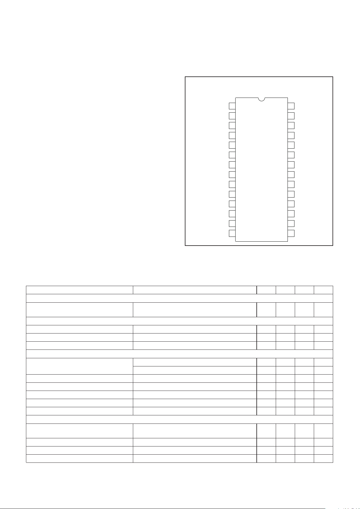
CONNECTION DIAGRAM
DIL-28, SOIC- 28 (Top
View)
ELECTRICAL CHARACTERISTICS: Unless otherwise stated, these specifications apply for T
A
= 0°C to 70°C for the
UCC3750, –40°C to +85°C for the UCC2750, RT = 14k, CT = 470pF, C
REF
= 0.1µF, FS0 = 0, FS1 = 0, VDD = 5V. TA=TJ.
PARAMETER TEST CONDITIONS MIN TYP MAX UNITS
VDD Supply
Supply Current - Active With 12V Supplied to V
CP
and Charge Pump
Disabled
0.5 1 mA
Internal Reference w/External Bypass
Output Voltage (REF) 7.3 7.55 7.8 V
Load Regulation I
REF
= 0mA – 2mA 30 60 mV
Line Regulation VCP = 10V to 13V, I
REF
= 1mA 3 15 mV
Amplifier
Input Voltage Error, DC Offset and Amp Amplifiers 2.9 3 3.1 V
DC Limit Amplifier 0.7125 0.75 0.7875 V
Input Bias Current 500 600 nA
AVOL V
OUT
= 2V to 4V 70 dB
VOH Source 100µA 5.35 6 7.0 V
VOL Sink 100µA 0.2 0.65 V
Short Circuit Current V
IN
= 0V and 5V with V
OUT
= 0V and 5V 0.5 2 3 mA
Sine Reference
Accuracy T
J
= 25°C, Program Frequency–Reference
Frequency
–1 0 1 Hz
Total Harmonic Distortion (Note 1) 2 %
Amplitude Peak 0.475 0.5 0.525 V
Offset 2.85 3.0 3.15 V
3
UCC2750
UCC3750
ELECTRICAL CHARACTERISTICS:
Unless otherwise stated, these specifications apply for TA= 0°C to 70°C for the
UCC3750, –40°C to +85°C for the UCC2750, RT = 14k, CT = 470pF, C
REF
= 0.1µF, FS0 = 0, FS1 = 0, VDD = 5V. TA=TJ.
PARAMETER TEST CONDITIONS MIN TYP MAX UNITS
Oscillator
Accuracy 108 128 148 kHz
Peak Voltage 4.6 4.75 4.9 V
Valley Voltage 2.9 3.05 3.2 V
Charge Pump
Switch Pull Up Resistance (VS1, VS2) 10 30 Ω
Switch Pull Down Resistance (VS1, VS2) 10 30 Ω
Output Voltage (VCP) VDD = 5V, I
VCP
= 10mA 11 12 14 V
Output Drivers
Pull Up Resistance 915Ω
Pull Down Resistance 915Ω
Rise Time CL = 2.7nF 50 100 ns
Fall Time CL = 2.7nF 50 100 ns
Current Limit
DC Limit Threshold Voltage Positive R5/R6 = 3 0.4 0.5 0.6 V
DC Limit Threshold Voltage Negative R5/R6 = 3 –0.6 –0.5 –0.4 V
Duty Cycle
Maximum PWM Duty Cycle 48 50 %
Rectifier Duty Cycle 50 %
Note 1: Guaranteed by measuring the steps of the PWL Sine Wave.
STATE % VCC VALUE FOR REF = 7.5 STATE % VCC VALUE FOR REF = 7.5
0 0.3333 2.5 5 0.4255 3.191
1 0.3384 2.538 6 0.4471 3.353
2 0.3528 2.646 7 0.4616 3.462
3 0.3745 2.808 8 0.4666 3.5
4 0.4 3
AMPIN: Inverting input of the uncommitted amplifier.
AMPOUT: Output of the uncommitted amplifier.
CT: This pin programs the internal PWM oscillator
frequency. Capacitor from CT to GND sets the charge
and discharge time of the oscillator.
ENBL: Logic input which enables the outputs and the
charge pump when high. ENBL should be pulled low to
turn the outputs off.
FS0, FS1: Frequency select pins for the internal
sine-wave generator. Table 1 provides the SINREF
frequencies as a function of FS0 and FS1 when a 32kHz
crystal is used at the crystal inputs (XTAL1, XTAL2).
Other proportional frequencies can be obtained with a
different crystal. Inputs FS0 and FS1 are TTL compatible.
Table I. Frequency selection table
(for 32kHz crystal).
FS0 FS1 SINREF (Hz)
00 20
10 25
01 50
1 1 High Impedance
GD1: Output driver that controls the primary side switch
in a flyback converter through a gate drive transformer.
The output signal on this pin is PWM during positive
power transfer modes and zero during negative power
transfer modes.
PIN DESCRIPTIONS

4
UCC2750
UCC3750
GD2: Output driver that controls the p-channel secondary
side switch in the flyback converter. The output signal on
this pin is PWM during mode 4 (Fig. 2) when the
reference signal is negative and power is being returned
to the input. This pin functions as a synchronous rectifier
output during mode 1 with positive reference signal and
positive power transfer. This output is logically inverted to
provide the correct polarity drive signal for a p-channel
switch.
GD3: Output driver that controls the n-channel secondary
side switch in the flyback converter. The output signal on
this pin is PWM during mode 2 (Fig. 2) when the
reference signal is positive and power is being returned
to the input. This pin functions as a synchronous rectifier
output during mode 3 with a negative reference signal
and positive power transfer.
GND: Reference point for the internal reference and all
thresholds. Also provides the signal return path for all
other pins.
NEG1: Inverting input of the buffer amplifier that acts as
a summing junction for the DC (battery) offset voltage
and sinewave reference.
NEG2: Inverting input of the error amplifier where the
ringer output voltage and the reference signal with the
desired offset are applied with a weighted sum.
Feedback compensation is connected between NEG2
and OUT2.
NEGDC: Inverting input of the amplifier used for DC
current limiting.
OUT1: Output of the buffer amplifier that provides scaling
and filtering for the reference signal before feeding it into
the error amplifier. This output is also used internally to
select the PWM mode for the flyback converter.
OUT2: Output of the error amplifier. Used to connect
compensation components. This output’s absolute value
determines the duty cycle of the PWM pulse. The polarity
of this signal also determines the PWM mode.
OUTDC: Output of the DC current limit amplifier. The DC
current limit is activated when this pin is above 4.5V or
below 1.5V.
REF: Internal 7.5V reference. For best results, bypass to
GND with a ceramic capacitor(>0.1µF).
RGOOD: Logic output that indicates that the error
amplifier output is within range (0< D< 0.5). This pin can
source upto 0.5mA of current.
RT: Resistor from RT to GND helps set the oscillator
frequency. RT programs the charge and discharge
currents of CT.
SINFLT: This signal is the buffered version of SINREF.
This signal is summed with the DC offset level with
appropriate scaling.
SINREF: This pin is the output of the sine-wave
reference generator. It has a high output impedance
(≈25kΩ). A 0.01µF capacitor to GND is recommended to
provide smoothing of the sinewave. When FS0 and FS1
are both set high, the sine reference generator is
disabled allowing this pin to accept an external sinewave
input.
SWRLY: Logic output that leads the battery offset
crossings (by typically 5ms) to allow “zero voltage” relay
switching. This pin can typically source 250µA.
XTAL1: Crystal connection for external crystal. This pin
can be also used to clock the internal sine wave
generator when XTAL2 is connected to VDD/2.
XTAL2: Crystal connection for external crystal.
VCP: External connection for charge pump storage
capacitor. A capacitance ≥2.2mF is recommended for
low charge pump output ripple. The voltage at this pin is
used by the output drivers for gate drive voltages.
Alternatively, a regulated gate drive voltage (>10V) can
be connected at this pin while leaving the charge pump
circuit at nodes VS1, VS2 disconnected.
VDD: External supply input used to bias internal logic
functions. Typically a regulated 5V supply is connected
between this pin and GND. It also is the input voltage for
the voltage tripler circuit to generate the gate drive
voltage.
VS1, VS2: Voltage switches for the voltage tripler
(charge pump circuit). They provide different voltage
PIN DESCRIPTIONS (cont.)

5
UCC2750
UCC3750
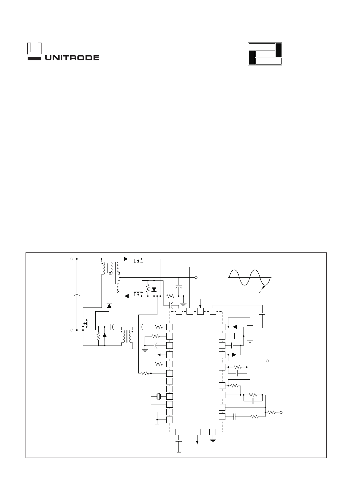
The UCC3750 provides complete control and protection
functions for a four quadrant flyback converter used to
generate ring signals for telephone circuits. A typical ap
plication circuit for a 15 REN ring generator is shown in
Fig. 1.
As shown, the flyback converter takes a DC input (typi
cally 48V) and provides an isolated output with a pro
grammable frequency (and amplitude) AC signal
superimposed on a programmable DC offset. The power
path consists of a primary side PWM switch Q1, primary
return rectifier DR1, a 4-winding transformer T1, output
rectifiers DR2 and DR3, synchronous/PWM switches Q2
and Q3, and output filter CF. Resistor R
SENSE provides
the output current sensing for protection circuits.
Different operating modes of the converter are depicted
in Table 2. Fig. 2 shows the output voltage and current
waveforms for a purely capacitive load and identifies the
four operating modes. Fig. 3 shows the PWM waveforms
for the circuit and Fig. 4a - 4d show the equivalent cir
cuits under the operating modes. The addition of Q2, Q3
and primary diode facilitates true four quadrant operation
where both the output voltage and power transfer can be
bi-directional. Mode 1 is similar to the commonly used
DC-DC converter operation where Q1 is modulated with
the PWM signal and rectification is provided through the
Q2, DR2 path to provide a positive output proportional to
the increasing, positive reference voltage. The
pulse-width is controlled by the error amplifier output to
increase or decrease the output as dictated by the refer
-
ence. The maximum duty cycle is limited to 50% to pre
-
vent DR1 from turning on prior to Q2/DR2.
In mode 2, the reference begins to decrease, necessitat
ing that the power transfer back to the input. For this
mode, switch Q3 needs to be modulated while DR1 acts
as the rectifier back to the input. The UCC3750 has
mode decoding circuitry which automatically directs the
PWM signal to Q3 and turns off Q1.
APPLICATION INFORMATION
18
21
22
15
FULLW AVE
RECTIFIER
MAG
SIGN
OUT2
MODE SIGN OUT1 OUT2 OUT3
0 0 PWM OFF RECIRC
01 PWMOFF
OFF OFF PWM
OFF
1
1
0
1 PWM RECIRC OFF
CONTROL LOGIC
REF
ERROR
AMP
V
CM
NEG2
17 16
OUT1
REF
DC OFFSET AMP
V
CM
NEG1
2
28
26
V
CP
V
CP
V
CP
GD1
GD2
GD3
MODE
SIGN
PWM
DC
CURRENT
LIMIT
SINE REFERENCE
GENERA T OR
REF
10
SINFLT
9
SINREF
20
FS0
8
SWRLY
19
FS1
XTAL
OSC
14
13
12
11
5
4
7
6
CHARGE
PUMP
INTERNAL
REFERENCE
REF=7.5V
V
CM
=3.0V
25
V
CM
3
GNDREF
VDD
VS2
VS1
NEGDC
VCP
OUTDC
V
CM
4
REF
AMPIN
AMPOUT
XTAL2
XTAL1
MAG
RAMP
CLOCK
GENERA T OR
24
RT
23
CT1RGOOD27ENBL
V
CM
AMP
V
CM
DETAILED BLOCK DIAGRAM
UDG-99074
Note: All pin numbers are for N or DW Packages.
Mode Reference
Polarity
Power
Flow
E.A.
Output
Source
(PWM)
Switch
Rectifier
Switch
1 + + – Q1 Q2
2 + – + Q3 (D1)
3 – + + Q1 Q3
4 – – – Q2 (D1)
Table II. Operating modes.

6
UCC2750
UCC3750
Figure 1. Typical application circuit.
APPLICATION INFORMATION (cont.)
UDG-99075
15
28
2
4
26 27 25
6
CR5
C10
2.2µF
C11 0.22
µF
CR7
5
C12 0.22
µF
7
18
16
17
10
R11 148k
C14 1nF
R12 2.7k
R13 62k
C16 2.2
µF
R15 15k
R14 3.3M
OUT2
NEG2
VS2
VDD
VS1
VCP
OUT1
NEG1
REF
ENBL
GD3
GD2
VDD
5V
SINFLT
C9
0.47µF
24
23
1
11
12
OUTDC
NEGDC
RT
RGOOD
CT
GD1
AMPOUT
XTAL1
XTAL2
13
14
22
21
AMPIN
FS0
FS1
20
19
R3
R4 16k
C7 470pF
C5
0.47µF
R5 30k
R6
10k
X1 32kHz
C6 0.1
µF
R2Q2
CR2
BYV99
R9
C4
1µF
250V
CR8
CR3 BYV26C Q3
CR1
BYV99
R18
VDD
C19
100µF
CR6
R25 10k
C13
1µF
C18
22µF
R26
R27
R10
148k
9 8 3
SINREF SWRLY
GND
C17
0.047µF
S4S1S3
S2
VDD
R17
CR12
IRF840
C20 R20
T1
10
7,9
6
4
5
1
T2
4
3
2
1
C3 0.1
µF
Q4
Q6
MPSA06
Q5
2N5457
3
2
1
3
2
1
3
2
1
R23
CR9
R1
10k
R22
C22
C2
100µF
C1
100µF
C23
0.47
µF
V
IN
RTN
REF
VB
REF
V
OUT
GND
2N7001DICT
R21 C21
CR10
MTP2P50E

7
UCC2750
UCC3750
Figure 2. Operating modes.
Figure 3. Circuit waveforms.
UDG-96172-1 UDG-96173
Figure 4a. Mode 1: Forward power transfer, positive
output.
Figure 4b. Mode 2: Reverse power transfer, positive
output.
UDG-96162-1
UDG-96163
When the reference signal goes from positive to nega
tive, a transition is made from mode 2 to mode 3. In
mode 3, the converter once again acts as a DC-DC
flyback converter (with negative output). Similar to mode
1, Q1 is controlled by the PWM output, however, the rec
tifying path is now through Q3/DR3 as the output polarity
is reversed. At the mode boundaries, there could be
some distortion which won’t affect the THD too much as
it is near zero crossings. Finally, as the reference signal
starts increasing towards zero, the direction of power
transfer is again reversed and Q2 is PWMed in mode 4.
It should be noted that in modes 2 and 3 when the refer
-
ence is decreasing, the phase of the feedback path is in
verted compared to the other two modes. Traditional
PWM methods will result in instability due to this charac
teristic. The UCC3750 separates the error signal magni
tude and polarity and determines the correct PWM signal
based on a separate mode determination circuit.
APPLICATION INFORMATION (cont.)
Figure 4c. Mode 3: Forward power transfer, negative
output.
UDG-96164-1
Figure 4d. Mode 4: Reverse power transfer, negative
output.
UDG-96165-1

8
UCC2750
UCC3750
Sine Reference Generator
The IC has a versatile low frequency sinewave reference
generator with low harmonic distortion and good fre
quency accuracy. In its intended mode as shown in Fig.
5, the reference generator will take an input from a
32kHz crystal (connected between XTAL1 and XTAL2)
and generate a sine-wave at 20Hz, 25Hz or 50Hz based
on the programming of pins FS0 and FS1 (See Table 2).
If the crystal frequency is changed, the output frequen
cies will be appropriately shifted. C-2 type Quartz crystals
(Epson makes available through DigiKey) are recom
mended for this application. If the frequency accuracy is
not a major concern, the more common and less expen
sive clock crystal (C-type) at 32.768kHz can be used with
a minor output frequency offset (20.5Hz instead of 20Hz).
Additionally, the XTAL1 input can be clocked at a desired
frequency to get a different set of output frequencies at
the sine-wave output (with divide ratios of 1600, 1280
and 640). The sine-wave output is centered around an internal reference of 3V. A capacitor from SINREF to GND
helps provide smoothing of the sine wave reference.
Recommended value is at least 0.01µF and maximum of
0.1µF. When FS0 and FS1 are both 1 (high), the sine reference is disabled and external sine-wave can be fed
into the SINREF pin. This signal should have the same
DC offset as the internal sine-wave (3V).
Reference and Error Amplifier
The recommended circuit connections for these circuits
are shown in Fig. 6. The sine-wave is added to a DC offset to create the composite reference signal for the error
amplifier. The DC reference can vary over a wide range.
For pure AC outputs it is zero, while in many common
applications, it is the talk battery voltage (–48V). The
UCC3750 accomplishes this task by summing the two
signals weighted by resisting R14 and R15. The output of
AMP1 also helps determine the mode of the circuit.
Referring to Fig. 6, the output of AMP1 is given by :
VOUT1= 1+
R13
R14
+
R13
R26
•VCM–
R13
R26
•REF
(1)
–
R13
R14
•VB–
R13
R15
• VAC
In order to nullify the effect of V
CM
on this value, the ratio
of R26 to R14 should be made 1.5. With this ratio, the
equation becomes:
VOUT1= VCM–
R13
R14
•VB–
R13
R15
• VAC
(2)
VOUT1 is the reference voltage that the second amplifier
(AMP2) uses to program the output voltage. Assuming
that Z4 is high DC impedance, the output voltage is de
rived by summing the currents into pin 18. The output is
given as:
VO = 1+
R10
R27
+
R10
R12
•VCM
(3)
–
R10
R27
•REF –
R10
R12
•VOUT1
Again, if the ratio of R27 to R10 is made 1.5, the effect of
V
CM is nullified and the output voltage becomes (after
substituting for VOUT1):
VO =
R10 •R13
R12 •R14
•VB+
R10 •R13
R12 •R15
• VAC
(4)
From equation 4, it can be seen that if the output voltage
DC value has to track VB directly, the following condition
should be forced:
R10 • R13 = R12 • R14 (5)
However, in some cases, this becomes impractical due
to large AC gain required form VACto VO.Only a small
part of the gain can be accommodated in the first ampli
fier stage due to its output voltage limitations. As a result,
the required resistance values become very high. This
APPLICATION INFORMATION (cont.)
Figure 5. Sine-wave generator. Figure 6. Error amplifier setup.
UDG-96166-1
UDG-96167-1

9
UCC2750
UCC3750
problem is only manifested for high values of VB (e.g.
48V) and can be alleviated by using a fraction of the re
quired DC offset as the VB input and regaining the offset
with resistive ratios.
The error amplifier compares the reference signal with
the output voltage by way of weighted sum at its invert
ing input. The error signal is further processed to sepa
rate its polarity and magnitude. An absolute value circuit
(precision full-wave rectifier) is used to get the magnitude
information. The polarity is used along with the reference
signal polarity to determine the mode information. The
absolute value circuit provides phase inversion when ap
propriate for modes 2 and 3 to maintain the correct loop
gain polarity. While the output of the error amplifier
swings around 3V, the full-wave rectifier output (MAG)
converts it into a signal above 3V. This signal is com
pared to the oscillator ramp to generate the PWM output.
Oscillator and PWM Comparator
The UCC3750 has an internal oscillator capable of high
frequency (>250kHz) operation. A resistor on the RT pin
programs the current that charges and discharges CT,
resulting in a triangular ramp waveform. Fig 7. shows the
oscillator hook-up circuit. The ramp peak and valley are
4.75V and 3V respectively. The nominal frequency is
given by:
f=
1
1.17 •RT • CT
OSC
The ramp waveform and the rectified output of the error
amplifier are compared by the PWM comparator to gen
erate the PWM signal. The PWM action is disabled on
the positive slope of the ramp signal. Leading edge mod
-
ulation turns on the PWM signal when the ramp signal
falls below MAG on the falling slope and turns it off at the
end of the clock cycle. This technique enables synchro
nized turn-on of the rectifier switches immediately after
the PWM pulse is turned off. The triangular nature of the
ramp ensures that the maximum duty cycle of the PWM
output is 50%, providing inherent current limiting.
Control Logic and Outputs
The PWM signal is processed through control logic which
takes into account the operating mode and output polar
ity to determine which output to modulate. The logic table
for the outputs is given in Table 2. For example, assume
that the reference signal is in the first quadrant (positive
and increasing). The output will lag the reference by a
certain delay and hence the error amp output will be pos
itive, resulting in SIGN = 0. The logic table indicates that
GD1 is modulated during this phase allowing power
transfer to increase the output voltage to keep up with
the reference. Increasing error (MAG) will result in larger
duty cycle and enable the output to increase and catch
up with the reference. If the output becomes higher than
the reference (as is likely in the second quadrant when
the reference is dropping), the SIGN becomes 1 and
GD3 is modulated to decrease the output level by transferring power to the input. At the boundary of the first and
second quadrant, there may be some switching back and
forth between modes as the reference slope crosses
through zero. Some of this switching can be eliminated
by judicious selection of error amplifier filtering and compensation components. In the first quadrant, when PWM
is applied to Q1, Q2 is turned on in the rectifier mode by
the clock signal to allow the flyback transformer flux to
APPLICATION INFORMATION (cont.)
24
23
CT
I
R
S
Q
R
I
R
C
T
RT
3V
I
R
R
T
4.75V
3.0V
Figure 7. Oscillator setup.
UDG-99077

10
UCC2750
UCC3750
reset (and to transfer power to the output). Operation in
quadrants 3 and 4 is symmetrical to the first two quad
rants with Q2 and Q3 interchanged. Note that the output
signal for Q2 is logically inverted to allow for driving the
p-channel switch. An n-channel switch can also be used
for Q2, but the drive circuit must be transformer isolated
and the polarity inverted. The outputs are designed for
high peak current drive and low internal impedance. In
isolated systems, GD1 must be coupled to Q1 using a
gate-drive transformer.
DC Current Limit
The DC current limit function provides protection against
short circuit conditions by limiting the maximum current
level and shutting off the PWM function when the limit
point is reached.
The DC limit is activated when DC out is below 0.5 V
CM
or above 1.5 • VCM. The DC current limit can be pro
grammed by setting:
R5
R6
=3
.
With this ratio, a symmetric DC limit with thresholds of
±0.5V is obtained. For other ratios, the positive and neg
ative voltage thresholds for current sense signal are
given by:
V (POS) =
V
4
•1-
R6
R5
SENSE
CM
V(NEG)=
V
4
•1-
5R6
R5
SENSE
CM
Even though the DC current is typically sensed in the
secondary, the currentl limit is applied fo the active PWM
switch at the time. For example, if Q1 is the PWM switch
and DCLIM is activated, the UCC3750 will prevent
trun-on for Q1 during the negative slope of the ramp (Fig.
2). The DC limit is functional on a cycle-by-cycle basis.
Charge Pump and Reference
The UCC3750 is designed to work on the secondary side
of an isolated power supply. It requires a 5V power supply with respect to its GND pin to operate. Note that the
GND pin of the IC is also the reference point of the ring
signal that is generated by the converter. If the converter
output is connected in series with any other voltage, it
should be ensured that the available supply voltage is
referenced to the converter output return. The IC along
with its associated charge pump components shown in
Fig. 9 generates all the other voltages the system re
-
quires. The UCC3750 typically requires about 5mA to op
erate without any loads on the drive outputs. The charge
pump capacitor should be large enough to keep the VCP
fairly constant when driving Q1-Q3 in the converter.
12
11
V
CM
TO
PWM
NEGDC
OUTDC
DC
R5
R6
R
SENSE
R6
4
Figure 8. Current limiting.
APPLICATION INFORMATION (cont.)
Figure 9. Charge pump circuits.
UDG-96170-1
-20
0
20
40
60
80
100
120
1 10 100 1000 10000 100000 10000001E+07
FREQUENCY (Hz)
MAGNITUDE (dB)
0
20
40
60
80
100
120
140
160
180
MAG.
PHASE
10k
100k 1M
10M
PHASE (Degree)
1000
10010
1
Figure 10. Frequency response to error amplifiers.
UNITRODE CORPORATION
7 CONTINENTAL BLVD. • MERRIMACK, NH 03054
TEL. (603) 424-2410 FAX (603) 424-3460

IMPORTANT NOTICE
T exas Instruments and its subsidiaries (TI) reserve the right to make changes to their products or to discontinue
any product or service without notice, and advise customers to obtain the latest version of relevant information
to verify, before placing orders, that information being relied on is current and complete. All products are sold
subject to the terms and conditions of sale supplied at the time of order acknowledgement, including those
pertaining to warranty, patent infringement, and limitation of liability.
TI warrants performance of its semiconductor products to the specifications applicable at the time of sale in
accordance with TI’s standard warranty. Testing and other quality control techniques are utilized to the extent
TI deems necessary to support this warranty. Specific testing of all parameters of each device is not necessarily
performed, except those mandated by government requirements.
CERT AIN APPLICATIONS USING SEMICONDUCTOR PRODUCTS MAY INVOLVE POTENTIAL RISKS OF
DEATH, PERSONAL INJURY, OR SEVERE PROPERTY OR ENVIRONMENTAL DAMAGE (“CRITICAL
APPLICATIONS”). TI SEMICONDUCTOR PRODUCTS ARE NOT DESIGNED, AUTHORIZED, OR
WARRANTED TO BE SUITABLE FOR USE IN LIFE-SUPPORT DEVICES OR SYSTEMS OR OTHER
CRITICAL APPLICATIONS. INCLUSION OF TI PRODUCTS IN SUCH APPLICA TIONS IS UNDERSTOOD T O
BE FULLY AT THE CUSTOMER’S RISK.
In order to minimize risks associated with the customer’s applications, adequate design and operating
safeguards must be provided by the customer to minimize inherent or procedural hazards.
TI assumes no liability for applications assistance or customer product design. TI does not warrant or represent
that any license, either express or implied, is granted under any patent right, copyright, mask work right, or other
intellectual property right of TI covering or relating to any combination, machine, or process in which such
semiconductor products or services might be or are used. TI’s publication of information regarding any third
party’s products or services does not constitute TI’s approval, warranty or endorsement thereof.
Copyright 2000, Texas Instruments Incorporated
 Loading...