

Datasheet UCC3915PWPTR, UCC3915PWP, UCC3915N, UCC3915DPTR, UCC3915DP Datasheet (Texas Instruments)
...
UCC2915
UCC3915
SLUS198A - FEBRUARY 2000
FEATURES
•
Integrated 0.15 Ohm Power
MOSFET
•
7V to 15V Operation
•
Digital Programmable Current Limit
from 0A to 3A
•
100
A ICCwhen Disabled
•
Programmable ON Time
•
Programmable Start Delay
•
Fixed 2% Duty Cycle
•
Thermal Shutdown
•
Fault Output Indicator
•
Maximum Output Current can be set
to 1A above the Programmed Fault
Level or to a full 4A
• Power SOIC and TSSOP, Low
Thermal Resistance Packaging
DESCRIPTION
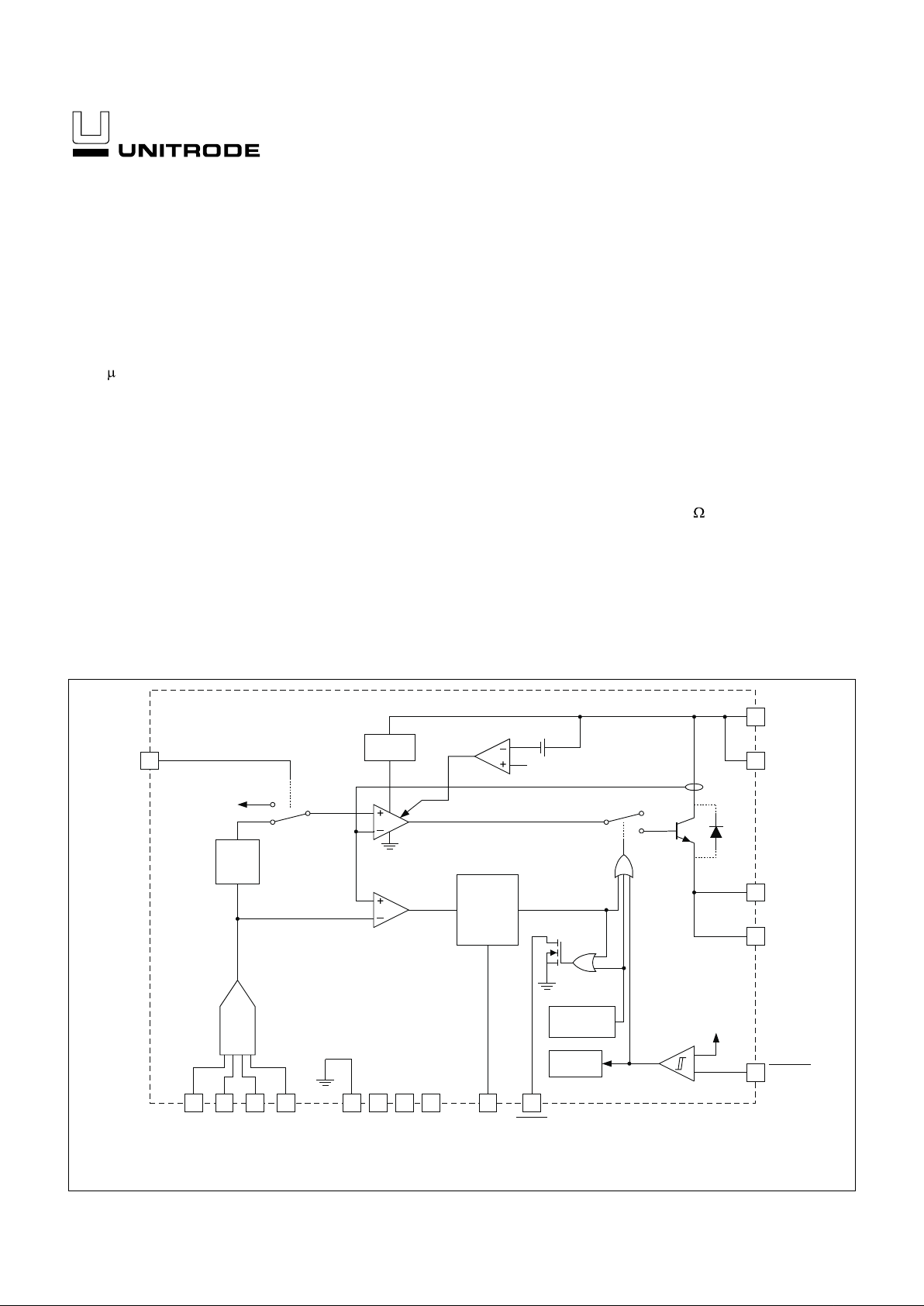
The UCC3915 Programmable Hot Swap Power Manager provides com
plete power management, hot swap capability, and circuit breaker functions.
The only external component required to operate the device, other than
power supply bypassing, is the fault timing capacitor, C
T
. All control and
housekeeping functions are integrated, and externally programmable.
These include the fault current level, maximum output sourcing current,
maximum fault time, and startup delay. In the event of a constant fault, the
Internal fixed 2% duty cycle ratio limits average output power.
The internal 4 bit DAC allows programming of the fault level current from 0
to 3A with 0.25A resolution. The IMAX control pin sets the maximum
sourcing current to 1A above the trip level or to a full 4A of output current
for fast output capacitor charging.
When the output current is below the fault level, the output MOSFET is
switched ON with a nominal ON resistance of 0.15
. When the output cur
rent exceeds the fault level, but is less than the maximum sourcing level,
the output remains switched ON, but the fault timer starts, charging CT.
Once CT charges to a preset threshold, the switch is turned OFF, and remains OFF for 50 times the programmed fault time. When the output current reaches the maximum sourcing level, the MOSFET transitions from a
switch to a constant current source.
6 7 8 9
1A
ABOVE
FAULT
OVER CURRENT
COMPARATOR
CURRENT FAULT
LEVEL 0–3 AMPS
10
H=4A
MAX
CURRENT
LEVEL
4A
ON TIME
CONTROL
2% DUTY
CYCLE
0–3A
0.25
RES
1113 1245
B3 B2 B1 B0
4BITDAC
GND
HEAT SINK
GND PINS
CT
CHARGE
PUMP
+
16
LINEAR CURRENT
AMPLIFIER
POWER
FET
2
3
V
OUT
REVERSE VOLTAGE
COMPARATOR
30mV
FAULT
THERMAL
SHUTDOWN
INTERNAL
BIAS
+
–
1
15
14
VOUT
VIN
CURRENT SENSE
H = OPEN
1.5V
SHTDWN
IMAX
*
*BODYDIODE
BLOCK DIAGRAM
15V Programmable Hot Swap Power Manager
UDG-99174
Note: Pin numbers refer to DIL-16 and SOIC-16 packages.
2
UCC2915
UCC3915
ABSOLUTE MAXIMUM RATINGS
VIN. . . . . . . . . . . . . . . . . . . . . . . . . . . . . . . . . . . . . . +15.5 Volts
VOUT
VIN. . . . . . . . . . . . . . . . . . . . . . . . . . . . . . . . . . . . .0.3V
FAULT
Sink Current. . . . . . . . . . . . . . . . . . . . . . . . . . . . . 50mA
FAULT
Voltage . . . . . . . . . . . . . . . . . . . . . . . . . . . . . 0.3 to 8V
Output Current . . . . . . . . . . . . . . . . . . . . . . . . . . . . Self Limiting
TTL Input Voltage . . . . . . . . . . . . . . . . . . . . . . . . . .
0.3 to V
IN
Storage Temperature . . . . . . . . . . . . . . . . . . . 65 C to +150 C
Junction Temperature. . . . . . . . . . . . . . . . . . .
55 C to +150 C
Lead Temperature (Soldering, 10 sec.). . . . . . . . . . . . . +300
C
Currents are positive into, negative out of the specified termi
-
nal. Consult Packaging Section of Databook for thermal limita
-
tions and considerations of packages.
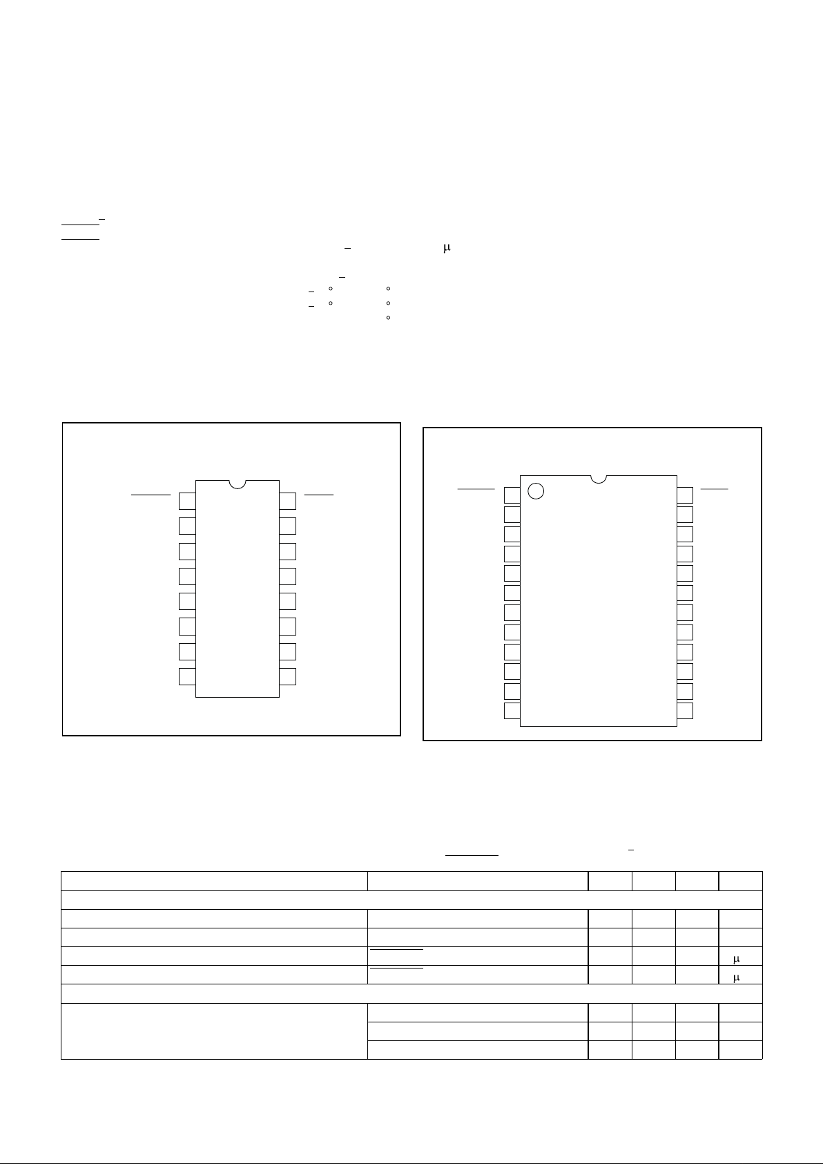
FAULT16
15
14
13
12
11
10
9
1
2
3
4
5
6
7
8
VOUT
VOUT
GND*
GND*
CT
IMAX
B0
SHTDWN
VIN
VIN
GND*
EGND*
B3
B2
B1
CONNECTION DIAGRAMS
*Pin 5 serves as lowest impedance to the electrical ground;
Pins 4, 12, and 13 serve as heat sink/ground. These pins
should be connected to large etch areas to help dissipate heat.
For N Package, pins 4, 12, and 13 are N/C.
(continued)
DESCRIPTION (cont.)
The UCC3915 can be put into sleep mode, drawing only
100
A of supply current. Other features include an open
drain Fault Output Indicator, Thermal Shutdown, Under
-
B3
N/C
N/C
GND*
GND*
FAULT
VIN
EGND*
GND*
GND*
VIN
N/C
GND*
SHTDWN
GND*
B2
GND*
GND*
CT
12
11
10
9
8
7
6
5
4
3
2
1
13
14
15
16
17
18
19
20
21
22
23
24
IMAX
VOUT
VOUT
B1 B0
*Pin 9 serves as lowest impedance to the electrical ground;
other GND pins serve as heat sink/ground. These pins should
be connected to large etch areas to help dissipate heat.
DIL-16, SOIC-16 (Top View)
N, DP Package
PWP-24 (Top View)
TSSOP Package
ELECTRICAL CHARACTERISTICS Unless otherwise stated, these specifications apply for TA = 40°C to +85°C for the
UCC2915 and 0°C to 70°C for the UCC3915, VIN = 12V, IMAX = 0.4V, SHTDWN
= 2.4V, TA=TJ.
PARAMETER TEST CONDITIONS MIN TYP MAX UNITS
Supply Section
Voltage Input Range 7.0 15.0 V
Supply Current 1.0 2.0 mA
Sleep Mode Current SHTDWN
= 0.2V, No load 100 150 A
Output Leakage SHTDWN
= 0.2V 20 A
Output Section
Voltage Drop I
OUT
= 1A (10V to 12V) 0.15 0.3 V
I
OUT
= 2A (10V to 12V) 0.3 0.6 V
I
OUT
= 3A (10V to 12V) 0.45 0.9 V

3
UCC2915
UCC3915
ELECTRICAL CHARACTERISTICS
Unless otherwise stated, these specifications apply for TA = 40°C to +85°C for the
UCC2915 and 0°C to 70°C for the UCC3915, VIN = 12V, IMAX = 0.4V, SHTDWN
= 2.4V, TA=TJ.
PARAMETER TEST CONDITIONS MIN TYP MAX UNITS
Output Section (cont.)
Voltage Drop (cont). I
OUT
= 1A, VIN = 7V and 15V 0.2 0.4 V
I
OUT
= 2A, VIN = 7V and 15V 0.4 0.8 V
I
OUT = 3A, VIN = 7V, 12V Max. 0.6 1.2 V
Initial Startup Time Note 2 100
s
Short Circuit Response Note 2 100 ns
Thermal Shutdown Note 2 165 °C
Thermal Hysteresis Note 2 10 °C
DAC Section
Trip Current Code = 0000-0011 (Device Off)
Code = 0100 0.07 0.25 0.45 A
Code = 0101 0.32 0.50 0.70 A
Code = 0110 0.50 0.75 0.98 A
Code = 0111 0.75 1.00 1.3 A
Code = 1000 1.0 1.25 1.6 A
Code = 1001 1.25 1.50 1.85 A
Code = 1010 1.5 1.75 2.15 A
Code = 1011 1.70 2.00 2.4 A
Code = 1100 1.90 2.25 2.7 A
Code = 1101 2.1 2.50 2.95 A
Code = 1110 2.30 2.75 3.25 A
Code = 1111 2.50 3.0 3.50 A
Max Output Current Over Trip (Current Source Mode) Code = 0100 to 1111, I
MAX
= 0V 0.35 1.0 1.65 A
Max Output Current (Current Source Mode) Code = 0100 to 1111, I
MAX
= 2.4V 3.0 4.0 5.2 A
Fault Output Section
CT Charge Current V
CT
= 1.0V 83 –62 47 A
CT Discharge Current V
CT
= 1.0V 0.8 1.2 1.8 A
Output Duty Cycle V
OUT
= 0V 1.0 1.9 3.3 %
CT Fault Threshold 1.2 1.5 1.7 V
CT Reset Threshold 0.4 0.5 0.6 V
Shutdown Section
Shutdown Threshold 1.1 1.5 1.9 V
Shutdown Hysteresis 150 mV
Input Current 100 500 nA
Open Drain Output Section
High Level Output Current FAULT
= 5V 250 A
Low Level Output Voltage I
OUT
= 5mA 0.2 0.8 V
TTL Input DC Characteristics Section
TTL Input Voltage High 2.0 V
TTL Input Voltage Low 0.8 V
TTL Input High Current V
IH
= 2.4V 3 10 A
TTL Input Low Current V
IL
= 0.4V 1 A
Note 1: All voltages are with respect to GND.Current is positive into and negative out of the specified terminal.
Note 2: Guaranteed by design.Not 100% tested in production.

4
UCC2915
UCC3915
9 8 7 61110
B3B2B1B0 IMAX
16
3
2
4 12 13 5
14
15
1SHTDWN
VOUTVIN
FAULT
CT
GND
HEAT SINK
GND PINS
UCC3915
R
L
C
OUT
V
OUT
C
SD
R
SD
V
IN
C
IN
LED
D1
C
T
S1 S2 S3 S4 S5
DIP
SWITCH
S6
V
IN
V
IN
R1
+5V
APPLICATIONS INFORMATION
Figure 1. Evaluation circuit.
UDG-99175
Protecting The UCC3915 From Voltage Transients
The parasitic inductance associated with the power distri
-
bution can cause a voltage spike at V
IN
if the load current
is suddenly interrupted by the UCC3915.
It is important to
limit the peak of this spike to less than 15V to prevent
damage to the UCC3915
. This voltage spike can be mini
-
mized by:
•
Reducing the power distribution inductance (e.g., twist
the positive (+) and negative (–) leads of the power
supply feeding V
IN
, locate the power supply close to
the UCC3915 or use a PCB ground plane).
•
Decoupling V
IN
with a capacitor, CIN(refer to Fig. 1),
located close to the V
IN
pin. This capacitor is typically
less than 1
F to limit the inrush current.
•
Clamping the voltage at V
IN
below 15V with a Zener
diode, D1(refer to Fig. 1), located close to the V
IN
pin.
PIN DESCRIPTIONS
SB0 - B3: These pins provide digital input to the DAC,
which sets the fault current threshold. They can be used
to provide a digital soft-start and adaptive current limiting.
CT: A capacitor connected to ground sets the maximum
fault time. The maximum fault time must be more than the
time required to charge the external capacitance in one
cycle. The maximum fault time is defined as T
FAULT
=
16.1
103CT. Once the fault time is reached the output
will shutdown for a time given by T
SD = 833 10
3
CT,
this equates to a 1.9% duty cycle.
FAULT
: Open drain output, which pulls low upon any fault
or interrupt condition, Fault, or Thermal Shutdown.
IMAX: When this pin is set to a logic low, the maximum
sourcing current will always be 1A above the pro
-
grammed fault level. When set to a logic high, the maxi
mum sourcing current will be a constant 4A for
applications which require fast charging of load capaci
tance.
SHTDWN
: When this pin is brought to a logic low, the IC
is put into a sleep mode drawing typically less than
100
AofICC.The input threshold is hysteretic, allowing
the user to program a startup delay with an external RC
circuit.
VIN: Input voltage to the UCC3915. The recommended
voltage range is 7 to 15 volts. Both VIN pins should be
connected together and connected to power source.
VOUT: Output voltage from the UCC3915. Both VOUT
pins should be connected together and connected to the
load. When switched the output voltage will be approxi
-
mately V
IN - (0.15 I
OUT
). VOUT must not exceed VIN
by greater than 0.3V.
5
UCC2915
UCC3915
APPLICATION INFORMATION (cont.)
Figure 2. Load current, timing capacitor voltage, and output voltage of the UCC3915 under fault conditions.
Estimating Maximum Load Capacitance
For hot swap applications, the rate at which the total
output capacitance can be charged depends on the
maximum output current available and the nature of the
load. For a constant-current, current-limited application,
the output will come up if the load asks for less than the
maximum available short-circuit current.
To guarantee recovery of a duty-cycle from a shortcircuited load condition, there is a maximum total output
capacitance which can be charged for a given unit ON
time (Fault time). The design value of ON or Fault time
can be adjusted by changing the timing capacitor C
T
.
For worst-case constant-current load of value just less
than the trip limit; C
OUT(max)
can be estimated from:
()
CII
C
V
OUT MAX LOAD
T
OUT
(max)
.
≈− •
••
16 1 10
3
Where V
OUT
is the output voltage.
For a resistive load of value R
I
, the value of C
OUT(max)
can be estimated from:
C
C
Rn
V
IR
OUT
T
L
OUT
MAX L
(max)
.≈••
•
−
•
16 1 10
1
1
3
UDG-94138
UNITRODE CORPORATION
7 CONTINENTAL BLVD. • MERRIMACK, NH 03054
TEL. 603-424-2410 • FAX 603-424-3460
Although the UCC3915 is designed to provide system
protection for all fault conditions, all integrated circuits
can ultimately fail short. For this reason, if the UCC3915
is intended for use in safety critical applications where
UL or some other safety rating is required, a redundant
safety device such as a fuse should be placed in series
with the device. The UCC3915 will prevent the fuse from
blowing for virtually all fault conditions, increasing sys
tem reliability and reducing maintenance cost, in addition
to providing the hot swap benefits of the device.
SAFETY RECOMMENDATIONS
 Loading...