

Datasheet UCC3895QTR, UCC3895N, UCC3895DWTR, UCC3895DW, UCC2895QTR Datasheet (Texas Instruments)
...
BiCMOS Advanced Phase Shift PWM Controller
application
INFO
available
UCC1895
UCC2895
UCC3895
FEATURES
Programmable Output Turn-on Delay
•
Adaptive Delay Set
•
Bidirectional Oscillator Synchronization
•
Capability for Voltage Mode or Current
•
Mode Control
Programmable Soft Start/Soft Stop
•
and Chip Disable via a Single Pin
0% to 100% Duty Cycle Control
•
7MHz Error Amplifier
•
Operation to 1MHz
•
Low Active Current Consumption
•
(5mA Typical @ 500kHz)
• Very Low Current Consumption
During Undervoltage Lock-out
(150µA typical)
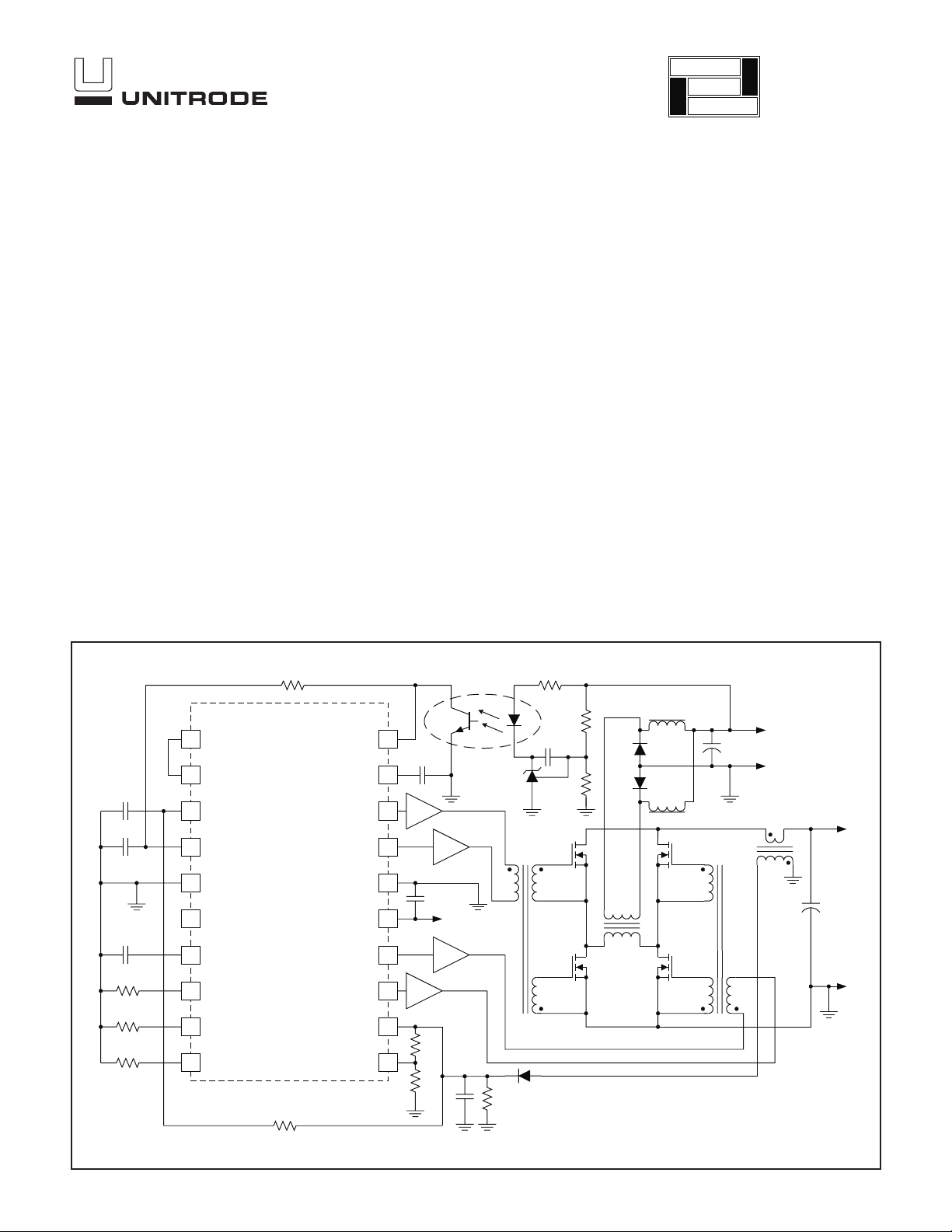
SIMPLIFIED APPLICATION DIAGRAM
DESCRIPTION
The UCC3895 is a phase shift PWM controller that implements control of a
full-bridge power stage by phase shifting the switching of one half-bridge
with respect to the other. It allows constant frequency pulse-width modula
tion in conjunction with resonant zero-voltage switching to provide high effi
ciency at high frequencies. The part can be used either as a voltage mode
or current mode controller.
While the UCC3895 maintains the functionality of the UC3875/6/7/8 family
and UC3879, it improves on that controller family with additional features
such as enhanced control logic, adaptive delay set, and shutdown capabil
ity. Since it is built in BCDMOS, it operates with dramatically less supply
current than it’s bipolar counterparts. The UCC3895 can operate with a
maximum clock frequency of 1MHz.
The UCC3895 and UCC2895 are offered in the 20 pin SOIC (DW) pack
age, 20 pin PDIP (N) package, 20 pin TSSOP (PW) package, and 20 pin
PLCC (Q). The UCC1895 is offered in the 20 pin CDIP (J) package, and 20
pin CLCC package (L).
-
-
-
-
UCC3895
EAN EAP
1
EAOUT
2
3
RAMP
4
REF
5
GND
6
SYNC
7
CT
8
RT
9
DELAB
10 11
DELCD ADS
SS/DISB
OUTA
OUTB
PGND
VCC
OUTC
OUTD
CS
Q1
77777777720
19
18
17
16
15
14
13
12
V
BIAS
AC
DB
V
OUT
V
IN
UDG-98139
SLUS157A - DECEMBER 1999
ABSOLUTE MAXIMUM RATINGS
Supply Voltage (IDD < 10mA) . . . . . . . . . . . . . . . . . . . . . . . 17V
Supply Current . . . . . . . . . . . . . . . . . . . . . . . . . . . . . . . . . 30mA
REF current . . . . . . . . . . . . . . . . . . . . . . . . . . . . . . . . . . . 15mA
OUT Current . . . . . . . . . . . . . . . . . . . . . . . . . . . . . . . . . . 100mA
Analog inputs
(EAP, EAN, EAOUT, RAMP,
SYNC, ADS, CS, SS/DISB) . . . . . . . . . . . –0.3V to REF+0.3V
Power Dissipation at T
Power Dissipation at T
Storage Temperature . . . . . . . . . . . . . . . . . . . –65°C to +150°C
Junction Temperature. . . . . . . . . . . . . . . . . . . –55°C to +125°C
Lead Temperature (soldering, 10 sec). . . . . . . . . . . . . . +300°C
Currents are positive into, negative out of the specified termi
nal. Consult Packaging Section of Databook for thermal limita
tions and considerations of package.
=+25°C (N Package). . . . . . . . . . . . 1W
A
=+25°C (D Package) . . . . . . . . 650mW
A
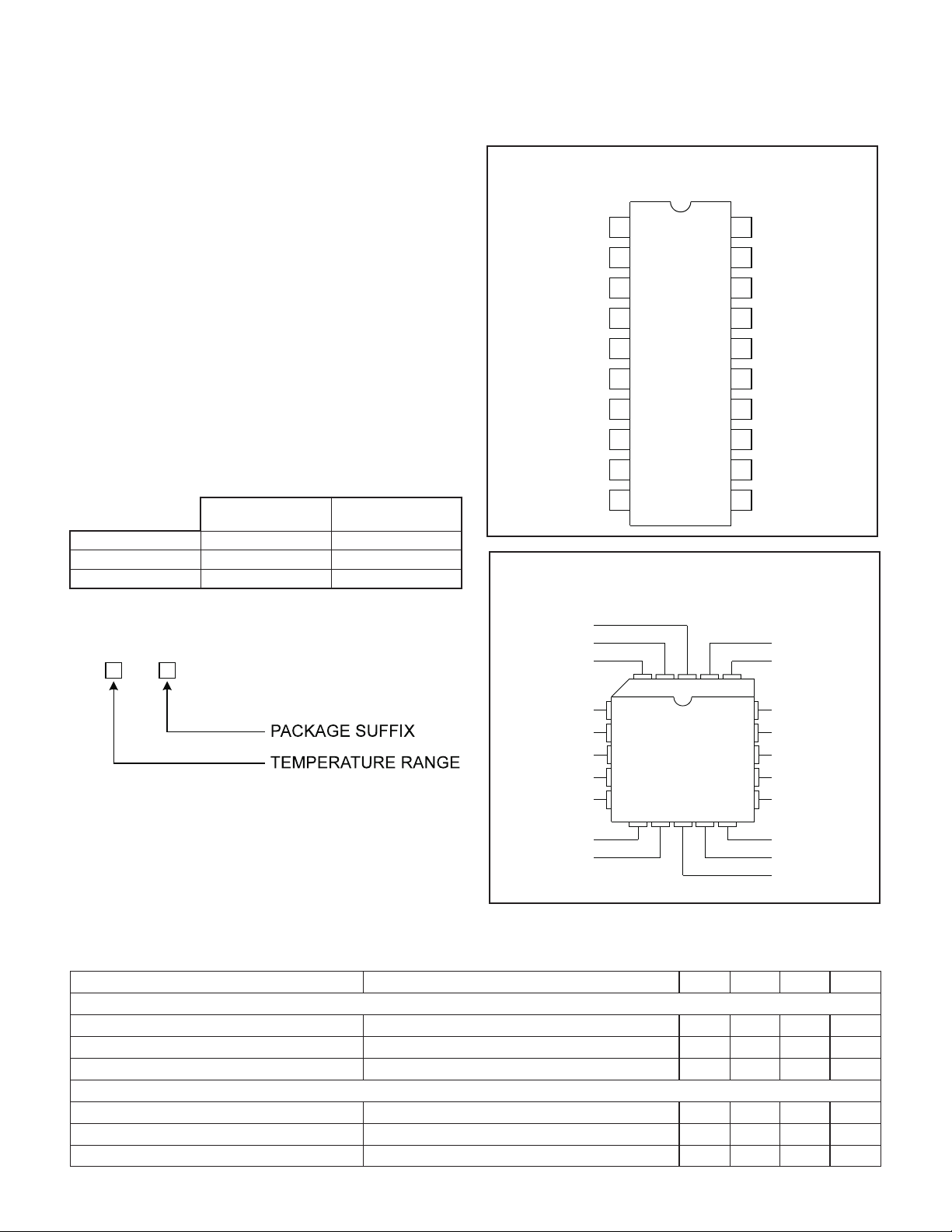
CONNECTION DIAGRAMS
DIL-20,c SOIC-20, TSSOP-20 (TOP VIEW)
J or N Package, DW Package, PW Package
EAN
1
EAOUT
RAMP
-
-
SYNC
REF
GND
CT
2
3
4
5
6
7
20
19
18
17
16
15
14
UCC1895
UCC2895
UCC3895
EAP
SS/DISB
OUTA
OUTB
PGND
VDD
OUTC
TEMPERATURE & PACKAGE SELECTION
TABLE
TEMPERATURE
RANGE
UCC1895 –55°C to +125°C J, L
UCC2895 –40°C to +85°C DW, N, PW, Q
UCC3895 0°C to +70°C DW, N, PW, Q
PACKAGE
SUFFIX
ORDERING INFORMATION
UCC 895
8
RT
DELAB CS
DELCD
9
10 ADS
PLCC-20, CLCC-20 (TOP VIEW)
Q Package, L Package
EAN
EAOUT
RAMP
3
122019
CT
RT
4
5
6
7
8
91110 12 13
REF
GND
SYNC
DELAB
DELCD
13
OUTD
12
11
EAP
SS/DISB
18
OUTA
17
OUTB
16
PGND
15
VDD
14
OUTC
OUTD
CS
ADS
ELECTRICAL CHARACTERISTICS:
RDELCD=10kΩ,C
=0.1µF, C
REF
=1.0µF, no load at outputs. TA=TJ. TA= 0°C to 70°C for UCC3895x, –40°C to +85°C for
VDD
Unless otherwise specified, VDD=12V, RT=82kΩ, CT=220pF, RDELAB=10kΩ,
UCC2895x, and –55°C to +125°C for UCC1895x.
PARAMETER TEST CONDITIONS MIN TYP MAX UNITS
UVLO Section
Start Threshold 10.2 11 11.8 V
Stop Threshold 8.2 9 9.8 V
Hysteresis 1.0 2.0 3.0 V
Supply Current
Start-up Current VDD = 8V 150 250
Active 56mA
I
DD
VDD Clamp Voltage IDD = 10mA 16.5 17.5 18.5 V
2
µA
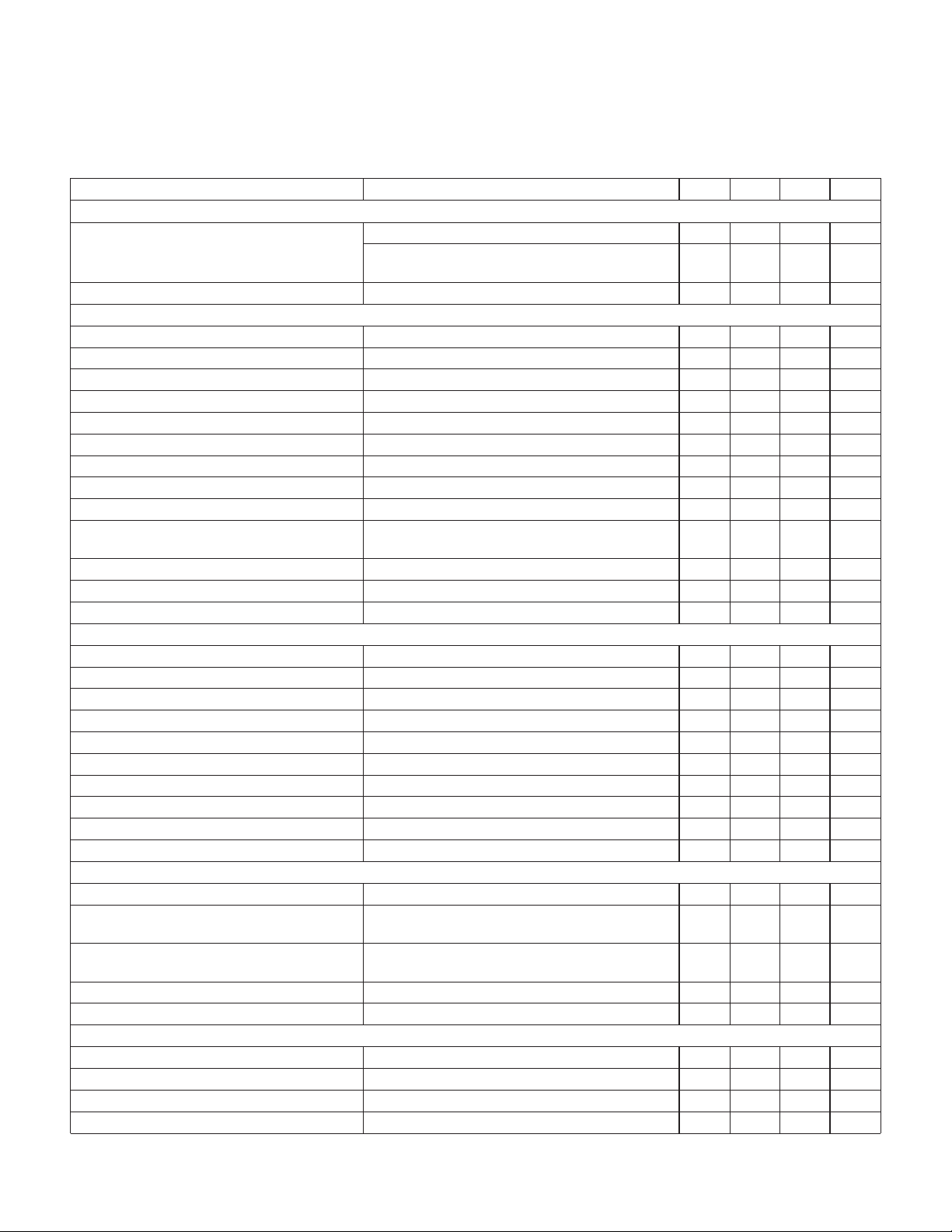
UCC1895
UCC2895
UCC3895
ELECTRICAL CHARACTERISTICS:
RDELCD=10kΩ,C
=0.1µF, C
REF
=1.0µF, no load at outputs. TA=TJ. TA= 0°C to 70°C for UCC3895x, –40°C to +85°C for
VDD
Unless otherwise specified, VDD=12V, RT=82kΩ, CT=220pF, RDELAB=10kΩ,
UCC2895x, and –55°C to +125°C for UCC1895x.
PARAMETER TEST CONDITIONS MIN TYP MAX UNITS
Voltage Reference Section
Output Voltage T
= 25°C 4.94 5.00 5.06 V
J
10V < VDD < 17.5V, 0mA < IREF < 5mA,
4.85 5 5.15 V
Temperature
Short Circuit Current REF = 0V, T
= 25°C 10 20 mA
J
Error Amplifier Section
Common Mode Input Voltage Range –0.1 3.6 V
Offset Voltage –7 7 mV
Input Bias Current (EAP, EAN) –1 1
EAOUT VOH EAP–EAN = 500mV, I
EAOUT VOL EAP–EAN = –500mV, I
= –0.5mA 4.0 4.5 5.0 V
EAOUT
= 0.5mA 0 0.2 0.4 V
EAOUT
EAOUT Source Current EAP–EAN = 500mV, EAOUT= 2.5V 1.0 1.5 mA
EAOUT Sink Current EAP–EAN = –500mV, EAOUT= 2.5V 2.5 4.5 mA
Open Loop DC Gain 75 85 dB
Unity Gain Bandwidth (Note 3) 5.0 7.0 MHz
Slew Rate EAN from 1V to 0V, EAP = 500mV,
1.5 2.2 V/
EAOUT from 0.5V to 3.0V
No Load Comparator Turn-Off Threshold 0.45 0.50 0.55 V
No Load Comparator Turn-On Threshold 0.55 0.60 0.69 V
No Load Comparator Hysteresis 0.035 0.100 0.165 V
Oscillator Section
Frequency T
= 25°C 473 500 527 kHz
J
Total Variation Line, Temperature (Note 3) 2.5 5 %
SYNC VIH 2.05 2.10 2.25 V
SYNC VIL 1.85 1.90 1.95 V
SYNC VOH I
SYNC VOL I
= –400µA, CT = 2.6V 4.1 4.5 5.0 V
SYNC
= 100µA, CT = 2.6V 0.0 0.5 1.0 V
SYNC
SYNC Output Pulse Width SYNC Load = 3.9kΩ and 30pF in parallel 85 135 ns
RT Voltage 2.9 3 3.1 V
CT Peak Voltage 2.25 2.35 2.50 V
CT Valley Voltage 0.0 0.2 0.4 V
PWM Comparator Section
EAOUT to RAMP Input Offset Voltage RAMP = 0V, DELAB = DELCD = REF 0.72 0.85 1.05 V
Minimum Phase Shift
RAMP = 0V, EAOUT = 650mV (Note 1) 0.00 0.85 1.40 %
(OUTA to OUTC, OUTB to OUTD)
RAMP to OUTC/OUTD Delay RAMP from 0V to 2.5V, EAOUT = 1.2V,
70 120 ns
DELAB = DELCD = REF (Note 2)
RAMP Bias Current RAMP < 5V, CT < 2.2V –5 5
RAMP Sink Current RAMP = 5V, CT < 2.6V 12 19 mA
Current Sense Section
CS Bias Current 0 < CS , 2.5V, 0 < ADS < 2.5V –4.5 20
Peak Current Threshold 1.90 2.00 2.10 V
Overcurrent Threshold 2.4 2.5 2.6 V
CS to Output Delay CS from 0 to 2.3V, DELAB = DELCD = REF 75 110 ns
µA
µs
µA
µA
3

UCC1895
UCC2895
UCC3895
ELECTRICAL CHARACTERISTICS:
RDELCD=10kΩ,C
=0.1µF, C
REF
=1.0µF, no load at outputs. TA=TJ. TA= 0°C to 70°C for UCC3895x, –40°C to +85°C for
VDD
Unless otherwise specified, VDD=12V, RT=82kΩ, CT=220pF, RDELAB=10kΩ,
UCC2895x, and –55°C to +125°C for UCC1895x.
PARAMETER TEST CONDITIONS MIN TYP MAX UNITS
Soft Start/Shutdown Section
Soft Start Source Current SS/DISB = 3.0V, CS < 1.9V –40 –35 –30
Soft Start Sink Current SS/DISB = 3.0V, CS > 2.6V 325 350 375
Soft Start/Disable Comparator Threshold 0.44 0.50 0.56 V
Delay Set Section
DELAB/DELCD Output Voltage ADS = CS = 0V 0.45 0.50 0.55 V
ADS = 0V, CS = 2.0V 1.9 2.0 2.1 V
Output Delay ADS = CS = 0V (Note 2) 450 525 600 ns
ADS Bias Current 0V < ADS < 2.5V, 0V < CS < 2.5V –20 20
Output Section
VOH (all outputs) IOUT = –10mA, VDD to Output 250 400 mV
VOL (all outputs) IOUT = 10mA 150 250 mV
Rise TIme C
Fall Time C
Note 1: Minimum phase shift is defined as followed:
Φ= •
200
tt
−
fOUTA fOUTC
()( )
t
PERIOD
Or
= 100pF 20 35 ns
LOAD
= 100pF 20 35 ns
LOAD
t
PERIOD
µA
µA
µA
Φ= •
200
t
t
t
t
t
= falling edge of OUTA signal
f(OUTA)
= falling edge of OUTB signal
f(OUTB)
= falling edge of OUTC signal
f(OUTC)
= falling edge of OUTD signal
f(OUTD)
(PERIOD)
tt
= period of OUTA or OUTB signal
−
fOUTB fOUTD
()()
t
PERIOD
where
Note 2. Output delay is measured between OUTA/OUTB or
OUTC/OUTD. Output delay is defined as shown below,
where:
t
t
= falling edge of OUTA signal
f(OUTA)
= rising edge of OUTB signal
r(OUTB)
Note 3: Guaranteed by design. Not 100% tested in production.
t
DELAY=tf(OUTA)–tf(OUTC)
Same applies to OUTB and OUTD
Same applies to OUTC and OUTD
OUTA
t
DELAY=tf(OUTA)–tr(OUTB)
OUTB
OUTA
OUTC
4

PIN DESCRIPTIONS
ADS: Adaptive Delay Set. This function sets the ratio be
tween the maximum and minimum programmed output
delay dead time. When the ADS pin is directly connected
to the CS pin, no delay modulation occurs. The maxi
mum delay modulation occurs when ADS is grounded. In
this case, delay time is four times longer when CS = 0
than when CS = 2.0V (the Peak Current threshold), ADS
changes the output voltage on the delay pins DELAB
and DELCD by the following formula:
VVVV
=•− +075 05..
[]
DEL CS ADS
where V
CS
and V
between 0V and 2.5V and must be less than or equal to
CS. DELAB and DELCD also will be clamped to a mini
mum of 0.5V.
EAOUT: Error Amplifier Output. It is also connected in
ternally to the non-inverting input of the PWM compara
tor and the no-load comparator. EAOUT is internally
clamped to the soft start voltage. The no-load comparator shuts down the output stages when EAOUT falls below 500mV, and allows the outputs to turn-on again
when EAOUT rises above 600mV.
CT: Oscillator Timing Capacitor. (Refer to Fig. 1, Oscillator Block Diagram) The UCC3895’s oscillator charges CT
via a programmed current. The waveform on C
sawtooth, with a peak voltage of 2.35V. The approximate
oscillator period is calculated by the following formula:
t
where C
seconds. C
5
=
OSC
is in Farads, and RTis in Ohms and t
T
T
note that a large C
sult in extended fall times on the C
creased fall time will increase the SYNC pulse width,
hence limiting the maximum phase shift between OUTA,
OUTB and OUTC, OUTD outputs, which limits the maxi
mum duty cycle of the converter.
CS: Current Sense. This is the inverting input of the Cur
rent Sense comparator and the non-inverting input of the
Over-current comparator, and the ADS amplifier. The
current sense signal is used for cycle-by-cycle current
limiting in peak current mode control, and for overcurrent
protection in all cases with a secondary threshold for out
put shutdown. An output disable initiated by an
overcurrent fault also results in a restart cycle, called
“soft stop”, with full soft start.
()
are in Volts. ADS must be limited to
ADS
T
RC
••
TT
48
can range from 100pF to 880pF. Please
and a small RTcombination will re
T
+
120
ns
OSC
waveform. The in
T
is a
is in
UCC1895
UCC2895
UCC3895
DELAB, DELCD: Delay Programming Between
Complementary Outputs. DELAB programs the dead
time between switching of OUTA and OUTB, and
DELCD programs the dead time between OUTC and
OUTD. This delay is introduced between complementary
outputs in the same leg of the external bridge. The
UCC3895 allows the user to select the delay, in which
the resonant switching of the external power stages
takes place. Separate delays are provided for the two
half-bridges to accommodate differences in resonant
capacitor charging currents. The delay in each stage is
set according to the following formula:
−
25 10
-
-
-
t
DELAY
where V
is in seconds. DELAB and DELCD can source about
()
=
is in Volts, and R
DEL
1mA maximum. Choose the delay resistors so that this
maximum is not exceeded. Programmable output delay
can be defeated by tying DELAB and/or DELCD to REF.
For an optimum performance keep stray capacitance on
these pins at <10pF.
EAP: The non-inverting input to the error amplifier.
EAN: The inverting input to the error amplifier.
GND: Chip ground for all circuits except the output
stages.
OUTA, OUTB, OUTC, OUTD: The 4 outputs are 100mA
complementary MOS drivers, and are optimized to drive
FET driver circuits. OUTA and OUTB are fully
complementary, (assuming no programmed delay). They
operate near 50% duty cycle and one-half the oscillating
frequency. OUTA and OUTB are intended to drive one
half-bridge circuit in an external power stage. OUTC and
OUTD will drive the other half-bridge and will have the
same characteristics as OUTA and OUTB. OUTC is
phase shifted with respect to OUTA, and OUTD is phase
shifted with respect to OUTB. Note that changing the
phase relationship of OUTC and OUTD with respect to
OUTA and OUTB requires other than the nominal 50%
duty ratio on OUTC and OUTD during those transients.
PGND: Output Stage Ground. To keep output switching
noise from critical analog circuits, the UCC3895 has 2
different ground connections. PGND is the ground
connection for the high-current output stages. Both GND
and PGND must be electrically tied together closely near
the IC. Also, since PGND carries high current, board
traces must be low impedance.
12
DEL
R
DEL
DEL
••
V
25
ns
+
is in Ohms and t
DELAY
5

PIN DESCRIPTIONS (cont.)
RAMP: The Inverting Input of the PWM Comparator.
This pin receives either the CT waveform in voltage and
average current mode controls, or the current signal
(plus slope compensation) in peak current mode control.
An internal discharge transistor is provided on RAMP,
which is triggered during the oscillator dead time.
RT: Oscillator Timing Resistor. (Refer to Fig. 1, Oscillator
Block Diagram) The oscillator in the UCC3895 operates
by charging an external timing capacitor, CT, with a fixed
current programmed by R
follows:
V
30.
I
=
RT
R
T
where R
is in Ohms and IRTis in Amperes. RTcan
T
range from 40kΩ to 120kΩ Soft start charging and dis
charging current are also programmed by I
SS/DISB: Soft Start/Disable. This pin combines the two
independent functions.
Disable Mode
: A rapid shutdown of the chip is
accomplished by any one of the following: externally
forcing SS/DISB below 0.5V, externally forcing REF
below 4V, V
dropping below the UNLO threshold, or
DD
an overcurrent fault is sensed (CS = 2.5V).
In the case of REF being pulled below 4V or an UVLO
condition, SS/DISB is actively pulled to ground via an
internal MOSFET switch. If an overcurrent is sensed,
SS/DISB will sink a current of (10 • I
falls below 0.5V.
Note that if SS/DISB is externally forced below 0.5V the
pin will start to source current equal to I
the only time the part switches into the low IDD current
mode is when the part is in undervoltage lockout.
current is calculated as
T.RT
RT
) until SS/DISB
RT
. Also note that
RT
.
UCC1895
UCC2895
UCC3895
Soft Start Mode:
passed, VDD is above the start threshold, and/or
SS/DISB falls below 0.5V during a soft stop, SS/DISB
will switch to a soft start mode. The pin will now source
current, equal to I
SS/DISB determines the soft start (and soft-start) time. In
addition, a resistor in parallel with the capacitor may be
used, limiting the maximum voltage on SS/DISB. Note
that SS/DISB will actively clamp the EAOUT pin voltage
to approximately the SS/DISB pin voltage during both
soft start, soft stop, and disable conditions.
SYNC: Oscillator Synchronization. (Refer to Fig. 1, Oscil
lator Block Diagram) This pin is bidirectional. When used
as an output, SYNC can be used as a clock, which is the
same as the chip’s internal clock. When used as an in
put, SYNC will override the chip’s internal oscillator and
act as it’s clock signal. This bidirectional feature allows
synchronization of multiple power supplies. The SYNC
signal will also internally discharge the CT capacitor and
any filter capacitors that are present on the RAMP pin.
The internal SYNC circuitry is level sensitive, with an input low threshold of 1.9V, and an input high threshold of
2.1V. A resistor as small as 3.9kΩ may be tied between
SYNC and GND to reduce the sync pulse width.
VDD: Power Supply. VDD must be bypassed with a minimum of a 1.0µF low ESR, low ESL capacitor to ground.
REF: 5V, ±1.2% voltage reference. The reference
supplies power to internal circuitry, and can also supply
up to 5mA to external loads. The reference is shut down
during undervoltage lock-out but is operational during all
other disable modes. For best performance, bypass with
a 0.1µF low ESR, low ESL capacitor to ground
After a fault or disable condition has
. A user-selected capacitor on
RT
-
-
6

BLOCK DIAGRAM
I
RT
CT
SYNC
RAMP
RT
8
8(IRT)
7
6
3
OSC
COMPARATOR
+
0.8V
Q
Q
PWM
UCC1895
UCC2895
UCC3895
VDD
S
D
Q
S
D
Q
R
Q
Q
R
DELAY A
DELAY B
15
OUTA
18
DELAB
9
17
OUTB
EAOUT
EAP
EAN
SS
CS
2
20
1
12
19
10(IRT)
2V
2.5V
I
RT
REF
ERROR
AMP
CURRENT SENSE
COMPARATOR
OVER CURRENT
COMPARATOR
HI=ON
HI=ON
NO LOAD
COMPARATOR
0.5V/
0.6V
Q
S
Q
R
COMPARATOR
0.5V
DISABLE
D
Q
S
Q
R
UVLO COMPARATOR
REFERENCE OK
DELAY C
DELAY D
ADAPTIVE DELAY
SET AMPLIFIER
COMPARATOR
11V/9V
4V
REF
0.5V
OUTC
14
10
DELCD
OUTD
13
16
PGND
11
ADS
REF
4
GND
5
UDG-98140
7

CIRCUIT DESCRIPTION
RT
R
I
RT
T
REF
UCC1895
UCC2895
UCC3895
V
REF
8I
RT
CT
C
T
SYNC
Figure 1. Oscillator block diagram.
0.5V
100K
CS
100K
ADS
75K
+
–
75K
2.5V
0.2V
–
+
–
+
S
Q
R
CLOCK
CLOCK
UDG-98141
REF
TO DELAY A
+
–
AND DELAY B
BLOCKS
DELAB
REF
Figure 2. Adaptive delay set block diagram.
TO DELAY C
+
–
AND DELAY D
BLOCKS
DELCD
UDG-98142
8

CIRCUIT DESCRIPTION (cont.)
V
BUSSED CURRENT
FROM ADS CIRCUIT
3.5V
DELAB/CD
FROM PAD
2.5V
CLOCK
Figure 3. Delay block diagram (one delay block per output).
REF
UCC1895
UCC2895
UCC3895
DELAYED
CLOCK
SIGNAL
UDG-98143
APPLICATION INFORMATION
CLOCK
RAMP
&
COMP
PWM
SIGNAL
OUTPUT A
OUTPUT B
OUTPUT C
OUTPUT D
Figure 4. UCC3895 timing diagram (no output delay shown).
9
UDG-98138

TYPICAL CHARACTERISTIC
UCC1895
UCC2895
UCC3895
2000
1800
1600
1400
1200
1000
800
600
OUTPUT DELAY (ns)
400
200
0
010203040
Vcs=0V Vcs=2V
RDEL (kΩ)
Figure 5. Delay programming: characterizes the
output delay between A/B, C/D.
1
0.95
0.9
RT=47K RT=62k RT=82k RT=100k
1600
1400
1200
1000
800
600
400
FREQUENCY (kHz)
200
0
100 1000
CT (pF)
Figure 8. Frequency vs. RT/CT (oscillator frequency).
Vdd=10V Vdd=12V Vdd=15V Vdd=17V
9
8
7
6
Idd (mA)
0.85
EAOUT TO RAMP OFFSET (V)
0.8
-60 -40 -20 0 20 40 60 80 100 120
TEMPERATURE (°C)
Figure 6. EAOUT to RAMP offset over temperature.
GAIN (dB) PHASE MARGIN (°C)
100
80
60
GAIN (dB)
40
20
0
1 100 10000 1000000
FREQUENCY (Hz)
200
160
120
80
40
0
Figure 7. Error amplifier gain/phase margin.
(DEGREES)
PHASE MARGIN
5
4
0 400 800 1200 1600
OSCILLATOR FREQUENCY (kHz)
Figure 9. Idd vs. Vdd / oscillator frequency (no
output loading).
Vdd=10V Vdd=12V Vdd=15V Vdd=17V
13
12
11
10
9
8
Idd (mA)
7
6
5
4
0 400 800 1200 1600
OSCILLATOR FREQUENCY (kHz)
Figure 10. Idd vs. Vdd / oscillator frequency (with
0.1nf output loads).
UNITRODE CORPORATION
7 CONTINENTAL BLVD. • MERRIMACK, NH 03054
TEL. (603) 424-2410 • FAX (603) 424-3460
10
 Loading...