

Datasheet UCC2813-0, UCC2813-1, UCC2813-2, UCC2813-3, UCC2813-4 Datasheet (TEXAS INSTRUMENTS)
...Page 1
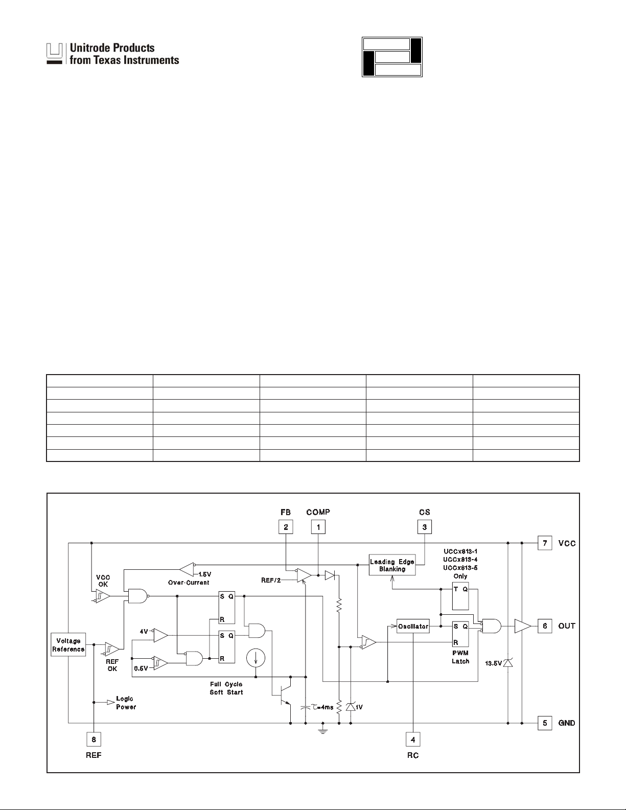
application
INFO
available
UCC2813-0/-1/-2/-3/-4/-5
UCC3813-0/-1/-2/-3/-4/-5
Low Power Economy BiCMOS Current Mode PWM
FEATURES
100mA Typical Starting Supply Current
•
500mA Typical Operating Supply Current
•
Operation to 1MHz
•
Internal Soft Start
•
Internal Fault Soft Start
•
Internal Leading-Edge Blanking of the
•
Current Sense Signal
1 Amp Totem-Pole Output
•
70ns Typical Response from
•
Current-Sense to Gate Drive Output
1.5% Tolerance Voltage Reference
•
Same Pinout as UCC3802, UC3842, and
•
UC3842A
DESCRIPTION
The UCC3813-0/-1/-2/-3/-4/-5 family of high-speed, low-power inte
grated circuits contain all of the control and drive components required
for off-line and DC-to-DC fixed frequency current-mode switching power
supplies with minimal parts count.
These devices have the same pin configuration as the UC3842/3/4/5
family, and also offer the added features of internal full-cycle soft start
and internal leading-edge blanking of the current-sense input.
The UCC3813-0/-1/-2/-3/-4/-5 family offers a variety of package options,
temperature range options, choice of maximum duty cycle, and choice
of critical voltage levels. Lower reference parts such as the UCC3813-3
and UCC3813-5 fit best into battery operated systems, while the higher
reference and the higher UVLO hysteresis of the UCC3813-2 and
UCC3813-4 make these ideal choices for use in off-line power supplies.
The UCC2813-x series is specified for operation from –40°C to +85°C
and the UCC3813-x series is specified for operation from 0°C to +70°C.
ORDERING INFORMATION
Part Number Maximum Duty Cycle Reference Voltage Turn-On Threshold Turn-Off Threshold
UCCx813-0 100% 5V 7.2V 6.9V
UCCx813-1 50% 5V 9.4V 7.4V
UCCx813-2 100% 5V 12.5V 8.3V
UCCx813-3 100% 4V 4.1V 3.6V
UCCx813-4 50% 5V 12.5V 8.3V
UCCx813-5 50% 4V 4.1V 3.6V
-
BLOCK DIAGRAM
SLUS161A - APRIL 1999 - REVISED JANUARY 2005
UDG-96134
Page 2
UCC2813-0/-1/-2/-3/-4/-5
UCC3813-0/-1/-2/-3/-4/-5
ABSOLUTE MAXIMUM RATINGS (Note 1)
VCC Voltage (Note 2) ........................... 12.0V
VCC Current................................. 30.0mA
OUT Current .................................. ±1.0A
OUT Energy (Capacitive Load) ................... 20.0mJ
Analog Inputs (FB, CS) ....................–0.3V to 6.3V
Power Dissipation at T
Power Dissipation at T
Storage Temperature ...................–65°C to +150°C
Junction Temperature...................–55°C to +150°C
Lead Temperature (Soldering, 10 Seconds)......... +300°C
Note 1: All voltages are with respect to GND. All currents are
positive into the specified terminal. Consult Unitrode Integrated
Circuits databook for information regarding thermal specifica
tions and limitations of packages.
Note 2: In normal operation VCC is powered through a current
limiting resistor. Absolute maximum of 12V applies when VCC
is driven from a low impedance source such that ICC does not
exceed 30mA. The resistor should be sized so that the VCC
voltage under operating conditions is below 12V but above the
turn off threshold.
UCC2813 –40°C TO +85°C N, D, PW
UCC3813 0°C TO +70°C N, D, PW
< +25°C (N Package)......... 1.0W
A
< +25°C (D Package)........ 0.65W
A
TEMPERATURE RANGE PACKAGES
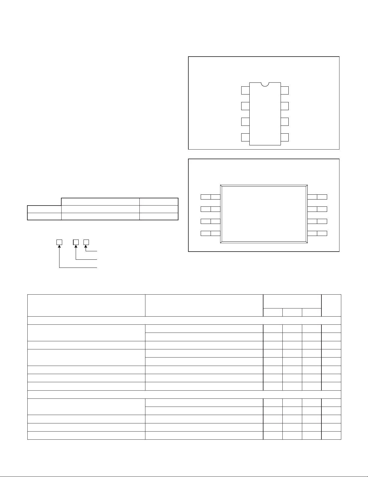
CONNECTION DIAGRAMS
DIL-8 or SOIC-8 (TOP VIEW)
N or D PACKAGE
COMP
FB
CS
-
TSSOP-8 (TOP VIEW)
PW PACKAGE
1
2
3
RC
COMP
FB
CS
1
2
3
4
REF
8
VCC
7
OUT
6
GND
5
REF
VCC
OUT
8
7
6
ORDERING INFORMATION
UCC
813
–
4
RC
GND
5
PRODUCT OPTION
PACKAGE
TEMPERATURE RANGE
ELECTRICAL CHARACTERISTICSUnless otherwise stated, these specifications apply for –40°C £ T
UCC2813-x; 0°C £ T
0.1mF capacitor from VCC to GND; 0.1mF capacitor from VREF to GND. T
£ +70°C for UCC3813-x; VCC = 10V (Note 3); RT = 100k from REF to RC; CT=330pF from RC to GND;
A
A=TJ
.
£ +85°C for
A
UCC2813-x
PARAMETER TEST CONDITIONS
UCC3813-x
MIN TYP MAX
Reference Section
Output Voltage T
= +25°C, I = 0.2mA, UCCx813-0/-1/-2/-4 4.925 5.00 5.075 V
J
T
= +25°C, I = 0.2mA, UCCx813-3/-5 3.94 4.00 4.06 V
J
Load Regulation 0.2mA <I<5mA 10 30 mV
Total Variation UCCx813 -0-1/-2/-4 (Note 7) 4.84 5.00 5.10 V
UCCx813-5 (Note 7) 3.84 4.00 4.08 V
Output Noise Voltage 10Hz £ f £ 10kHz, T
Long Term Stability T
= +125°C, 1000 Hours (Note 9) 5 mV
A
= +25°C (Note 9) 70 mV
J
Output Short Circuit –5 –35 mA
Oscillator Section
Oscillator Frequency UCCx813-0/-1/-2/-4 (Note 4) 40 46 52 kHz
UCCx813-3/-5 (Note 4) 26 31 36 kHz
Temperature Stability (Note 9) 2.5 %
Amplitude Peak-to-Peak 2.25 2.40 2.55 V
Oscillator Peak Voltage 2.45 V
UNITS
2
Page 3
UCC2813-0/-1/-2/-3/-4/-5
UCC3813-0/-1/-2/-3/-4/-5
ELECTRICAL CHARACTERISTICS
UCC2813-x; 0°C £ T
0.1mF capacitor from VCC to GND; 0.1mF capacitor from VREF to GND. T
Error Amplifier Section
Input Voltage COMP = 2.5V; UCCx813-0/-1/-2/-4 2.42 2.50 2.56 V
Input Bias Current
Open Loop Voltage Gain 60 80 dB
COMP Sink Current FB = 2.7V, COMP = 1.1V 0.4 2.5 mA
COMP Source Current FB = 1.8V, COMP = REF – 1.2V –0.2 –0.5 –0.8 mA
Gain Bandwidth Product (Note 9) 2 MHz
PWM Section
Maximum Duty Cycle UCCx813-0/-2/-3 97 99 100 %
Minimum Duty Cycle COMP = 0V 0 %
Current Sense Section
Gain (Note 5) 1.10 1.65 1.80 V/V
Maximum Input Signal COMP = 5V (Note 6) 0.9 1.0 1.1 V
Input Bias Current
CS Blank Time 50 100 150 ns
Over-Current Threshold 1.32 1.55 1.70 V
COMP to CS Offset CS = 0V 0.45 0.90 1.35 V
Output Section
OUT Low Level I = 20mA, all parts 0.1 0.4 V
OUT High V
(VCC-OUT)
Rise Time C
Fall Time C
Undervoltage Lockout Section
Start Threshold (Note 8) UCCx813-0 6.6 7.2 7.8 V
Stop Threshold (Note 8) UCC1813-0 6.3 6.9 7.5 V
Start to Stop Hysteresis UCCx813-0 0.12 0.3 0.48 V
SAT
£ +70°C for UCC3813-x; VCC = 10V (Note 3); RT = 100k from REF to RC; CT=330pF from RC to GND;
A
PARAMETER TEST CONDITIONS
Unless otherwise stated, these specifications apply for –40°C £ TA£ +85°C for
.
A=TJ
UCC2813-x
UCC3813-x
MIN TYP MAX
COMP = 2.0V; UCCx813-3/-5 1.92 2.0 2.05 V
–22mA
UCCx813-1/-4/-5 48 49 50 %
–200 200 nA
I = 200mA, all parts 0.35 0.90 V
I = 50mA, VCC = 5V, UCCx813-3/-5 0.15 0.40 V
I = 20mA, VCC = 0V, all parts 0.7 1.2 V
I = –20mA, all parts 0.15 0.40 V
I = –200mA, all parts 1.0 1.9 V
I = –50mA,VCC = 5V, UCCx813-3/-5 0.4 0.9 V
= 1nF 41 70 ns
L
= 1nF 44 75 ns
L
UCCx813-1 8.6 9.4 10.2 V
UCCx813-2/-4 11.5 12.5 13.5 V
UCCx813-3/-5 3.7 4.1 4.5 V
UCC1813-1 6.8 7.4 8.0 V
UCCx813-2/-4 7.6 8.3 9.0 V
UCCx813-3/-5 3.2 3.6 4.0 V
UCCx813-1 1.6 2 2.4 V
UCCx813-2/-4 3.5 4.2 5.1 V
UCCx813-3/-5 0.2 0.5 0.8 V
UNITS
3
Page 4
UCC2813-0/-1/-2/-3/-4/-5
UCC3813-0/-1/-2/-3/-4/-5
ELECTRICAL CHARACTERISTICS
UCC2813-x; 0°C £ T
0.1mF capacitor from VCC to GND; 0.1mF capacitor from VREF to GND. T
Soft Start Section
COMP Rise Time FB = 1.8V, Rise from 0.5V to REF–1V 4 ms
Overall Section
Start-up Current VCC < Start Threshold 0.1 0.23 mA
Operating Supply Current FB = 0V, CS = 0V, RC = 0V 0.5 1.2 mA
VCC Internal Zener Voltage ICC = 10mA (Note 8) 12 13.5 15 V
VCC Internal Zener Voltage Minus Start
Threshold Voltage
Note 3: Adjust VCC above the start threshold before setting at 10V.
Note 4: Oscillator frequency for the UCCx813-0, UCCx813-2 and UCCx813-3 is the output frequency.
Oscillator frequency for the UCCx813-1, UCCx813-4 and UCCx813-5 is twice the output frequency.
Note 5: Gain is defined by:
Note 6: Parameter measured at trip point of latch with Pin 2 at 0V.
Note 7: Total Variation includes temperature stability and load regulation.
Note 8: Start Threshold, Stop Threshold and Zener Shunt Thresholds track one another.
Note 9: Ensured by design. Not 100% tested in production.
£ +70°C for UCC3813-x; VCC = 10V (Note 3); RT = 100k from REF to RC; CT=330pF from RC to GND;
A
PARAMETER TEST CONDITIONS
V
D
COMP
A
=££
D
Unless otherwise stated, these specifications apply for –40°C £ TA£ +85°C for
.
A=TJ
UCC2813-x
UCC3813-x
MIN TYP MAX
UCCx813-2/-4 0.5 1.0 V
VV
008.
V
CS
CS
.
UNITS
PIN DESCRIPTIONS
COMP: COMP is the output of the error amplifier and the
input of the PWM comparator.
Unlike other devices, the error amplifier in the UCC3813
family is a true, low output-impedance, 2MHz operational
amplifier. As such, the COMP terminal can both source
and sink current. However, the error amplifier is internally
current limited, so that you can command zero duty cycle
by externally forcing COMP to GND.
The UCC3813 family features built-in full cycle Soft Start.
Soft Start is implemented as a clamp on the maximum
COMP voltage.
FB: FB is the inverting input of the error amplifier. For
best stability, keep FB lead length as short as possible
and FB stray capacitance as small as possible.
CS: CS is the input to the current sense comparators.
The UCC3813 family has two different current sense
comparators: the PWM comparator and an over-current
comparator.
The UCC3813 family contains digital current sense filter
ing, which disconnects the CS terminal from the current
sense comparator during the 100ns interval immediately
following the rising edge of the OUT pin. This digital filter
ing, also called leading-edge blanking, means that in
most applications, no analog filtering (RC filter) is re
quired on CS. Compared to an external RC filter tech
nique, the leading-edge blanking provides a smaller
effective CS to OUT propagation delay. Note, however,
that the minimum non-zero On-Time of the OUT signal is
directly affected by the leading-edge-blanking and the
CS to OUT propagation delay.
The over-current comparator is only intended for fault
sensing, and exceeding the over-current threshold will
cause a soft start cycle.
RC: RC is the oscillator timing pin. For fixed frequency
operation, set timing capacitor charging current by con
necting a resistor from REF to RC. Set frequency by con
necting a timing capacitor from RC to GND. For best
performance, keep the timing capacitor lead to GND as
short and direct as possible. If possible, use separate
ground traces for the timing capacitor and all other func
tions.
-
-
-
-
-
-
4
Page 5
PIN DESCRIPTIONS (cont.)
The frequency of oscillation can be estimated with the
following equations:
UCCx813-0/-1/-2/-4:
UCCx813-3, UCCx813-5:
where frequency is in Hz, resistance is in W, and capaci
tance is in farads. The recommended range of timing re
sistors is between 10k and 200k and timing capacitor is
100pF to 1000pF. Never use a timing resistor less than
10k.
GND: GND is reference ground and power ground for all
functions on this part.
OUT:OUT is the output of a high-current power driver ca
pable of driving the gate of a power MOSFET with peak
currents exceeding ±750mA. OUT is actively held low
when VCC is below the UVLO threshold.
The high-current power driver consists of FET output devices, which can switch all of the way to GND and all of
the way to VCC. The output stage also provides a very
low impedance to overshoot and undershoot. This
means that in many cases, external schottky clamp diodes are not required.
VCC: VCC is the power input connection for this device.
In normal operation VCC is powered through a current
limiting resistor. Although quiescent VCC current is very
F
=
15.
RC
·
F
=
10.
RC
·
UCC2813-0/-1/-2/-3/-4/-5
UCC3813-0/-1/-2/-3/-4/-5
low, total supply current will be higher, depending on
OUT current. Total VCC current is the sum of quiescent
VCC current and the average OUT current. Knowing the
operating frequency and the MOSFET gate charge (Qg),
average OUT current can be calculated from:
=·
IQF
OUT g
To prevent noise problems, bypass VCC to GND with a
-
0.1 mF ceramic capacitor in parallel as close to the VCC
-
pin as possible. An electrolytic capacitor may also be
used in addition to the ceramic capacitor.
REF: REF is the voltage reference for the error amplifier
and also for many other functions on the IC. REF is also
used as the logic power supply for high speed switching
logic on the IC.
-
When VCC is greater than 1V and less than the UVLO
threshold, REF is pulled to ground through a 5kW resis
tor. This means that REF can be used as a logic output
indicating power system status. It is important for reference stability that REF is bypassed to GND with a ceramic capacitor as close to the pin as possible. An
electrolytic capacitor may also be used in addition to the
ceramic capacitor. A minimum of 0.1mF ceramic is required. Additional REF bypassing is required for external
loads greater than 2.5mA on the reference.
To prevent noise problems with high speed switching
transients, bypass REF to ground with a ceramic capacitor very close to the IC package.
.
-
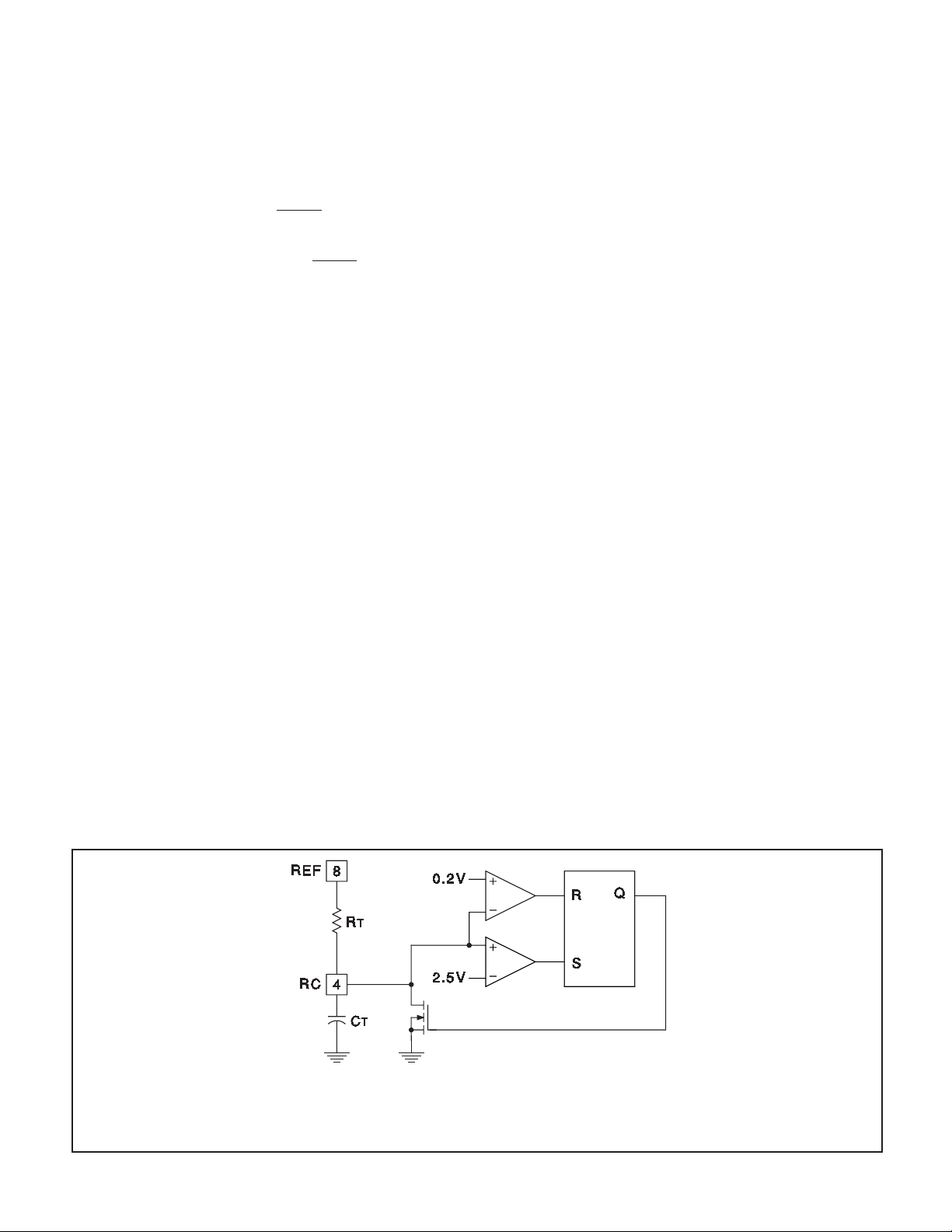
APPLICATION INFORMATION
UDG-96139
The UCC3813-0/-1/-2/-3/-4/-5 oscillator generates a sawtooth waveform on RC. The rise time is set by the time constant of R
and CT. The fall time is set by CT and an internal transistor on-resistance of approximately 125W. During the fall time, the out
put is off and the maximum duty cycle is reduced below 50% or 100% depending on the part number. Larger timing capacitors
increase the discharge time and reduce the maximum duty cycle and frequency.
Figure 1. Oscillator.
5
T
-
Page 6
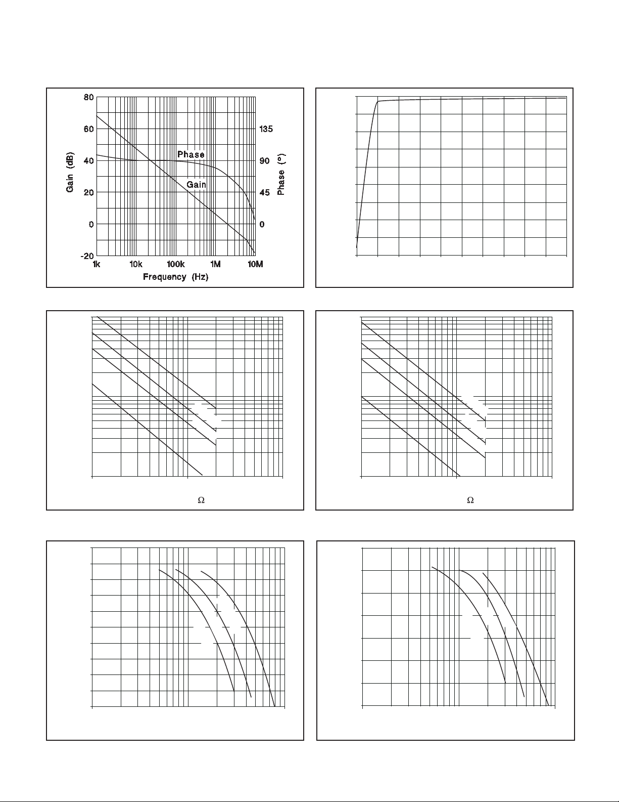
APPLICATION INFORMATION (cont.)
REF
V (V)
UCC2813-0/-1/-2/-3/-4/-5
UCC3813-0/-1/-2/-3/-4/-5
4.00
3.98
3.96
3.94
3.92
3.90
3.88
3.86
3.84
1000
100pF
100
200pF
Oscillator Freq. (kHz)
330pF
1nF
10
10 100 1000
R(k)
T
Figure 3. UCC3813-0/-1/-2/-4 oscillator frequency vs. R
and C
.
T
100
99.5
99
98.5
98
97.5
97
96.5
Maximum Duty Cycle (%)
96
95.5
95
10 100 1000
Oscillator Frequency (kHz)
C = 200pF
T
C = 330pF
T
C = 100pF
T
Figure 4. UCC3813-0/-2/-3 max. duty cycle vs. oscillator
frequency.
3.82
V (V)
vs. VCC;I
REF
5
5.2 5.4 5.6 5.8 6
CC
LOAD
4 4.2 4.4 4.6 4.8
Figure 5. UCC3813-3/-5 V
1000
100
Oscillator Freq. (kHz)
100pF
200pF
330pF
1nF
10
10 100 1000
R(k)
T
Figure 6. UCC3813-3/-5 oscillator frequency vs. RTand
T
.
C
T
50
49.5
49
48.5
48
47.5
Maximum Duty Cycle (%)
47
46.5
10 100 1000
Oscillator Frequency (kHz)
C = 200pF
T
C = 330pF
T
C = 100pF
T
Figure 7. UCC3813-1/-4/-5 max. duty cycle vs. oscillator
frequency.
6
= 0.5mA.Figure 2. Error amplifier gain/phase response.
Page 7

APPLICATION INFORMATION (cont.)
UCC2813-0/-1/-2/-3/-4/-5
UCC3813-0/-1/-2/-3/-4/-5
16
14
12
CC
I (mA)
10
8
6
4
2
CC
V = 10V, 1nF
CC
V = 8V, 1nF
CC
V = 10V, No Load
CC
V = 8V, No Load
0
0 100 200 300 400 500 600 700 800 900 1000
Oscillator Frequency (kHz)
Figure 8. UCC3813-0 ICCvs. oscillator frequency.
500
450
400
350
300
250
200
Dead Time (ns)
150
100
50
0
100 200 300 400 500 600 700 800 900 1000
C (pF)
T
UCC1803/5
UCC1800/1/2/4
8
7
6
CC
V = 10V, 1nF
CC
V = 8V, 1nF
CC
V = 10V, No Load
CC
V = 8V, No Load
CC
I (mA)
5
4
3
2
1
0
0 100 200 300 400 500 600 700 800 900 1000
Oscillator Frequency (kHz)
Figure 10. UCC3813-5 ICCvs. oscillator frequency.
1.1
1.0
0.9
0.8
0.7
COMP to CS Offset (Volts)
0.6
0
-55-50 -25 0 25 50 75 100 125
Temperature (°C)
Slope = 1.8mV/ C
°
Figure 9. Dead time vs. CT,RT= 100k.
Figure 11. COMP to CS offset vs. temperature,
CS=0V.
7
Page 8

PACKAGE OPTION ADDENDUM
www.ti.com
PACKAGING INFORMATION
Orderable Device Status
UCC2813D-0 ACTIVE SOIC D 8 75 Green (RoHS &
UCC2813D-0G4 ACTIVE SOIC D 8 75 Green (RoHS &
UCC2813D-1 ACTIVE SOIC D 8 75 Green (RoHS &
UCC2813D-1G4 ACTIVE SOIC D 8 75 Green (RoHS &
UCC2813D-2 ACTIVE SOIC D 8 75 Green (RoHS &
UCC2813D-2G4 ACTIVE SOIC D 8 75 Green (RoHS &
UCC2813D-3 ACTIVE SOIC D 8 75 Green (RoHS &
UCC2813D-3G4 ACTIVE SOIC D 8 75 Green (RoHS &
UCC2813D-4 ACTIVE SOIC D 8 75 Green (RoHS &
UCC2813D-4G4 ACTIVE SOIC D 8 75 Green (RoHS &
UCC2813D-5 ACTIVE SOIC D 8 75 Green (RoHS &
UCC2813D-5G4 ACTIVE SOIC D 8 75 Green (RoHS &
UCC2813DTR-0 ACTIVE SOIC D 8 2500 Green (RoHS &
UCC2813DTR-0G4 ACTIVE SOIC D 8 2500 Green (RoHS &
UCC2813DTR-1 ACTIVE SOIC D 8 2500 Green (RoHS &
UCC2813DTR-1G4 ACTIVE SOIC D 8 2500 Green (RoHS &
UCC2813DTR-2 ACTIVE SOIC D 8 2500 Green (RoHS &
UCC2813DTR-2G4 ACTIVE SOIC D 8 2500 Green (RoHS &
UCC2813DTR-3 ACTIVE SOIC D 8 2500 Green (RoHS &
UCC2813DTR-3G4 ACTIVE SOIC D 8 2500 Green (RoHS &
UCC2813DTR-4 ACTIVE SOIC D 8 2500 Green (RoHS &
UCC2813DTR-4G4 ACTIVE SOIC D 8 2500 Green (RoHS &
UCC2813DTR-5 ACTIVE SOIC D 8 2500 Green (RoHS &
UCC2813DTR-5G4 ACTIVE SOIC D 8 2500 Green (RoHS &
UCC2813N-0 ACTIVE PDIP P 8 50 Green (RoHS &
(1)
Package
Type
Package
Drawing
Pins Package
Qty
Eco Plan
no Sb/Br)
no Sb/Br)
no Sb/Br)
no Sb/Br)
no Sb/Br)
no Sb/Br)
no Sb/Br)
no Sb/Br)
no Sb/Br)
no Sb/Br)
no Sb/Br)
no Sb/Br)
no Sb/Br)
no Sb/Br)
no Sb/Br)
no Sb/Br)
no Sb/Br)
no Sb/Br)
no Sb/Br)
no Sb/Br)
no Sb/Br)
no Sb/Br)
no Sb/Br)
no Sb/Br)
no Sb/Br)
(2)
Lead/Ball Finish MSL Peak Temp
CU NIPDAU Level-1-260C-UNLIM
CU NIPDAU Level-1-260C-UNLIM
CU NIPDAU Level-1-260C-UNLIM
CU NIPDAU Level-1-260C-UNLIM
CU NIPDAU Level-1-260C-UNLIM
CU NIPDAU Level-1-260C-UNLIM
CU NIPDAU Level-1-260C-UNLIM
CU NIPDAU Level-1-260C-UNLIM
CU NIPDAU Level-1-260C-UNLIM
CU NIPDAU Level-1-260C-UNLIM
CU NIPDAU Level-1-260C-UNLIM
CU NIPDAU Level-1-260C-UNLIM
CU NIPDAU Level-1-260C-UNLIM
CU NIPDAU Level-1-260C-UNLIM
CU NIPDAU Level-1-260C-UNLIM
CU NIPDAU Level-1-260C-UNLIM
CU NIPDAU Level-1-260C-UNLIM
CU NIPDAU Level-1-260C-UNLIM
CU NIPDAU Level-1-260C-UNLIM
CU NIPDAU Level-1-260C-UNLIM
CU NIPDAU Level-1-260C-UNLIM
CU NIPDAU Level-1-260C-UNLIM
CU NIPDAU Level-1-260C-UNLIM
CU NIPDAU Level-1-260C-UNLIM
CU NIPDAU N / A for Pkg Type
3-Mar-2008
(3)
Addendum-Page 1
Page 9
PACKAGE OPTION ADDENDUM
www.ti.com
Orderable Device Status
(1)
Package
Type
Package
Drawing
Pins Package
Qty
Eco Plan
UCC2813N-0G4 ACTIVE PDIP P 8 50 Green (RoHS &
(2)
Lead/Ball Finish MSL Peak Temp
CU NIPDAU N / A for Pkg Type
no Sb/Br)
UCC2813N-1 ACTIVE PDIP P 8 50 Green (RoHS &
CU NIPDAU N / A for Pkg Type
no Sb/Br)
UCC2813N-1G4 ACTIVE PDIP P 8 50 Green (RoHS &
CU NIPDAU N / A for Pkg Type
no Sb/Br)
UCC2813N-2 ACTIVE PDIP P 8 50 Green (RoHS &
CU NIPDAU N / A for Pkg Type
no Sb/Br)
UCC2813N-2G4 ACTIVE PDIP P 8 50 Green (RoHS &
CU NIPDAU N / A for Pkg Type
no Sb/Br)
UCC2813N-3 ACTIVE UTR TBD Call TI Call TI
UCC2813N-4 ACTIVE PDIP P 8 50 Green (RoHS &
CU NIPDAU N / A for Pkg Type
no Sb/Br)
UCC2813N-4G4 ACTIVE PDIP P 8 50 Green (RoHS &
CU NIPDAU N / A for Pkg Type
no Sb/Br)
UCC2813N-5 ACTIVE PDIP P 8 50 Green (RoHS &
CU NIPDAU N / A for Pkg Type
no Sb/Br)
UCC2813N-5G4 ACTIVE PDIP P 8 50 Green (RoHS &
CU NIPDAU N / A for Pkg Type
no Sb/Br)
UCC2813PW-0 ACTIVE TSSOP PW 8 150 Green (RoHS &
Call TI Level-2-260C-1 YEAR
no Sb/Br)
UCC2813PW-0G4 ACTIVE TSSOP PW 8 150 Green (RoHS &
Call TI Level-2-260C-1 YEAR
no Sb/Br)
UCC2813PW-1 ACTIVE TSSOP PW 8 150 Green (RoHS &
CU NIPDAU Level-2-260C-1 YEAR
no Sb/Br)
UCC2813PW-1G4 ACTIVE TSSOP PW 8 150 Green (RoHS &
CU NIPDAU Level-2-260C-1 YEAR
no Sb/Br)
UCC2813PW-2 ACTIVE TSSOP PW 8 150 Green (RoHS &
CU NIPDAU Level-2-260C-1 YEAR
no Sb/Br)
UCC2813PW-2G4 ACTIVE TSSOP PW 8 150 Green (RoHS &
CU NIPDAU Level-2-260C-1 YEAR
no Sb/Br)
UCC2813PW-3 ACTIVE TSSOP PW 8 150 Green (RoHS &
CU NIPDAU Level-2-260C-1 YEAR
no Sb/Br)
UCC2813PW-3G4 ACTIVE TSSOP PW 8 150 Green (RoHS &
CU NIPDAU Level-2-260C-1 YEAR
no Sb/Br)
UCC2813PW-4 ACTIVE TSSOP PW 8 150 Green (RoHS &
CU NIPDAU Level-2-260C-1 YEAR
no Sb/Br)
UCC2813PW-4G4 ACTIVE TSSOP PW 8 150 Green (RoHS &
CU NIPDAU Level-2-260C-1 YEAR
no Sb/Br)
UCC2813PW-5 ACTIVE TSSOP PW 8 150 Green (RoHS &
CU NIPDAU Level-2-260C-1 YEAR
no Sb/Br)
UCC2813PW-5G4 ACTIVE TSSOP PW 8 150 Green (RoHS &
CU NIPDAU Level-2-260C-1 YEAR
no Sb/Br)
UCC2813PWTR-0 ACTIVE TSSOP PW 8 2000 Green (RoHS &
CU NIPDAU Level-2-260C-1 YEAR
no Sb/Br)
UCC2813PWTR-0G4 ACTIVE TSSOP PW 8 2000 Green (RoHS &
CU NIPDAU Level-2-260C-1 YEAR
no Sb/Br)
UCC2813PWTR-1 ACTIVE TSSOP PW 8 2000 Green (RoHS &
CU NIPDAU Level-2-260C-1 YEAR
no Sb/Br)
UCC2813PWTR-1G4 ACTIVE TSSOP PW 8 2000 Green (RoHS &
CU NIPDAU Level-2-260C-1 YEAR
no Sb/Br)
3-Mar-2008
(3)
Addendum-Page 2
Page 10

PACKAGE OPTION ADDENDUM
www.ti.com
Orderable Device Status
(1)
Package
Type
Package
Drawing
Pins Package
Qty
Eco Plan
(2)
UCC2813PWTR-2 ACTIVE TSSOP PW 8 2000 Green (RoHS &
no Sb/Br)
UCC2813PWTR-2G4 ACTIVE TSSOP PW 8 2000 Green (RoHS &
no Sb/Br)
UCC2813PWTR-3 ACTIVE TSSOP PW 8 2000 Green (RoHS &
no Sb/Br)
UCC2813PWTR-3G4 ACTIVE TSSOP PW 8 2000 Green (RoHS &
no Sb/Br)
UCC2813PWTR-4 ACTIVE TSSOP PW 8 2000 Green (RoHS &
no Sb/Br)
UCC2813PWTR-4G4 ACTIVE TSSOP PW 8 2000 Green (RoHS &
no Sb/Br)
UCC2813PWTR-5 ACTIVE TSSOP PW 8 2000 Green (RoHS &
no Sb/Br)
UCC2813PWTR-5G4 ACTIVE TSSOP PW 8 2000 Green (RoHS &
no Sb/Br)
UCC3813D-0 ACTIVE SOIC D 8 75 Green (RoHS &
no Sb/Br)
UCC3813D-0G4 ACTIVE SOIC D 8 75 Green (RoHS &
no Sb/Br)
UCC3813D-1 ACTIVE SOIC D 8 75 Green (RoHS &
no Sb/Br)
UCC3813D-1G4 ACTIVE SOIC D 8 75 Green (RoHS &
no Sb/Br)
UCC3813D-2 ACTIVE SOIC D 8 75 Green (RoHS &
no Sb/Br)
UCC3813D-2G4 ACTIVE SOIC D 8 75 Green (RoHS &
no Sb/Br)
UCC3813D-3 ACTIVE SOIC D 8 75 Green (RoHS &
no Sb/Br)
UCC3813D-3G4 ACTIVE SOIC D 8 75 Green (RoHS &
no Sb/Br)
UCC3813D-4 ACTIVE SOIC D 8 75 Green (RoHS &
no Sb/Br)
UCC3813D-4G4 ACTIVE SOIC D 8 75 Green (RoHS &
no Sb/Br)
UCC3813D-5 ACTIVE SOIC D 8 75 Green (RoHS &
no Sb/Br)
UCC3813D-5G4 ACTIVE SOIC D 8 75 Green (RoHS &
no Sb/Br)
UCC3813DTR-0 ACTIVE SOIC D 8 2500 Green (RoHS &
no Sb/Br)
UCC3813DTR-0G4 ACTIVE SOIC D 8 2500 Green (RoHS &
no Sb/Br)
UCC3813DTR-1 ACTIVE SOIC D 8 2500 Green (RoHS &
no Sb/Br)
UCC3813DTR-1G4 ACTIVE SOIC D 8 2500 Green (RoHS &
no Sb/Br)
UCC3813DTR-2 ACTIVE SOIC D 8 2500 Green (RoHS &
no Sb/Br)
UCC3813DTR-2G4 ACTIVE SOIC D 8 2500 Green (RoHS &
no Sb/Br)
3-Mar-2008
Lead/Ball Finish MSL Peak Temp
CU NIPDAU Level-2-260C-1 YEAR
CU NIPDAU Level-2-260C-1 YEAR
CU NIPDAU Level-2-260C-1 YEAR
CU NIPDAU Level-2-260C-1 YEAR
CU NIPDAU Level-2-260C-1 YEAR
CU NIPDAU Level-2-260C-1 YEAR
CU NIPDAU Level-2-260C-1 YEAR
CU NIPDAU Level-2-260C-1 YEAR
CU NIPDAU Level-1-260C-UNLIM
CU NIPDAU Level-1-260C-UNLIM
CU NIPDAU Level-1-260C-UNLIM
CU NIPDAU Level-1-260C-UNLIM
CU NIPDAU Level-1-260C-UNLIM
CU NIPDAU Level-1-260C-UNLIM
CU NIPDAU Level-1-260C-UNLIM
CU NIPDAU Level-1-260C-UNLIM
CU NIPDAU Level-1-260C-UNLIM
CU NIPDAU Level-1-260C-UNLIM
CU NIPDAU Level-1-260C-UNLIM
CU NIPDAU Level-1-260C-UNLIM
CU NIPDAU Level-1-260C-UNLIM
CU NIPDAU Level-1-260C-UNLIM
CU NIPDAU Level-1-260C-UNLIM
CU NIPDAU Level-1-260C-UNLIM
CU NIPDAU Level-1-260C-UNLIM
CU NIPDAU Level-1-260C-UNLIM
(3)
Addendum-Page 3
Page 11

PACKAGE OPTION ADDENDUM
www.ti.com
Orderable Device Status
(1)
Package
Type
Package
Drawing
Pins Package
Qty
Eco Plan
(2)
UCC3813DTR-3 ACTIVE SOIC D 8 2500 Green (RoHS &
no Sb/Br)
UCC3813DTR-3G4 ACTIVE SOIC D 8 2500 Green (RoHS &
no Sb/Br)
UCC3813DTR-4 ACTIVE SOIC D 8 2500 Green (RoHS &
no Sb/Br)
UCC3813DTR-4G4 ACTIVE SOIC D 8 2500 Green (RoHS &
no Sb/Br)
UCC3813DTR-5 ACTIVE SOIC D 8 2500 Green (RoHS &
no Sb/Br)
UCC3813DTR-5G4 ACTIVE SOIC D 8 2500 Green (RoHS &
no Sb/Br)
UCC3813N-0 ACTIVE PDIP P 8 50 Green (RoHS &
no Sb/Br)
UCC3813N-0G4 ACTIVE PDIP P 8 50 Green (RoHS &
no Sb/Br)
UCC3813N-1 ACTIVE PDIP P 8 50 Green (RoHS &
no Sb/Br)
UCC3813N-1G4 ACTIVE PDIP P 8 50 Green (RoHS &
no Sb/Br)
UCC3813N-2 ACTIVE PDIP P 8 50 Green (RoHS &
no Sb/Br)
UCC3813N-2G4 ACTIVE PDIP P 8 50 Green (RoHS &
no Sb/Br)
UCC3813N-3 ACTIVE PDIP P 8 50 Green (RoHS &
no Sb/Br)
UCC3813N-3G4 ACTIVE PDIP P 8 50 Green (RoHS &
no Sb/Br)
UCC3813N-4 ACTIVE PDIP P 8 50 Green (RoHS &
no Sb/Br)
UCC3813N-4G4 ACTIVE PDIP P 8 50 Green (RoHS &
no Sb/Br)
UCC3813N-5 ACTIVE PDIP P 8 50 Green (RoHS &
no Sb/Br)
UCC3813N-5G4 ACTIVE PDIP P 8 50 Green (RoHS &
no Sb/Br)
UCC3813PW-0 ACTIVE TSSOP PW 8 150 Green (RoHS &
no Sb/Br)
UCC3813PW-0G4 ACTIVE TSSOP PW 8 150 Green (RoHS &
no Sb/Br)
UCC3813PW-1 ACTIVE TSSOP PW 8 150 Green (RoHS &
no Sb/Br)
UCC3813PW-1G4 ACTIVE TSSOP PW 8 150 Green (RoHS &
no Sb/Br)
UCC3813PW-2 ACTIVE TSSOP PW 8 150 Green (RoHS &
no Sb/Br)
UCC3813PW-2G4 ACTIVE TSSOP PW 8 150 Green (RoHS &
no Sb/Br)
UCC3813PW-3 ACTIVE TSSOP PW 8 150 Green (RoHS &
no Sb/Br)
UCC3813PW-3G4 ACTIVE TSSOP PW 8 150 Green (RoHS &
no Sb/Br)
3-Mar-2008
Lead/Ball Finish MSL Peak Temp
CU NIPDAU Level-1-260C-UNLIM
CU NIPDAU Level-1-260C-UNLIM
CU NIPDAU Level-1-260C-UNLIM
CU NIPDAU Level-1-260C-UNLIM
CU NIPDAU Level-1-260C-UNLIM
CU NIPDAU Level-1-260C-UNLIM
CU NIPDAU N / A for Pkg Type
CU NIPDAU N / A for Pkg Type
CU NIPDAU N / A for Pkg Type
CU NIPDAU N / A for Pkg Type
CU NIPDAU N / A for Pkg Type
CU NIPDAU N / A for Pkg Type
CU NIPDAU N / A for Pkg Type
CU NIPDAU N / A for Pkg Type
CU NIPDAU N / A for Pkg Type
CU NIPDAU N / A for Pkg Type
CU NIPDAU N / A for Pkg Type
CU NIPDAU N / A for Pkg Type
CU NIPDAU Level-2-260C-1 YEAR
CU NIPDAU Level-2-260C-1 YEAR
CU NIPDAU Level-2-260C-1 YEAR
CU NIPDAU Level-2-260C-1 YEAR
CU NIPDAU Level-2-260C-1 YEAR
CU NIPDAU Level-2-260C-1 YEAR
CU NIPDAU Level-2-260C-1 YEAR
CU NIPDAU Level-2-260C-1 YEAR
(3)
Addendum-Page 4
Page 12

PACKAGE OPTION ADDENDUM
www.ti.com
Orderable Device Status
(1)
Package
Type
Package
Drawing
Pins Package
Qty
Eco Plan
UCC3813PW-4 ACTIVE TSSOP PW 8 150 Green (RoHS &
(2)
Lead/Ball Finish MSL Peak Temp
CU NIPDAU Level-2-260C-1 YEAR
3-Mar-2008
(3)
no Sb/Br)
UCC3813PW-4G4 ACTIVE TSSOP PW 8 150 Green (RoHS &
CU NIPDAU Level-2-260C-1 YEAR
no Sb/Br)
UCC3813PW-5 ACTIVE TSSOP PW 8 150 Green (RoHS &
CU NIPDAU Level-2-260C-1 YEAR
no Sb/Br)
UCC3813PW-5G4 ACTIVE TSSOP PW 8 150 Green (RoHS &
CU NIPDAU Level-2-260C-1 YEAR
no Sb/Br)
UCC3813PWTR-0 ACTIVE TSSOP PW 8 2000 Green (RoHS &
CU NIPDAU Level-2-260C-1 YEAR
no Sb/Br)
UCC3813PWTR-0G4 ACTIVE TSSOP PW 8 2000 Green (RoHS &
CU NIPDAU Level-2-260C-1 YEAR
no Sb/Br)
UCC3813PWTR-1 ACTIVE TSSOP PW 8 2000 Green (RoHS &
CU NIPDAU Level-2-260C-1 YEAR
no Sb/Br)
UCC3813PWTR-1G4 ACTIVE TSSOP PW 8 2000 Green (RoHS &
CU NIPDAU Level-2-260C-1 YEAR
no Sb/Br)
UCC3813PWTR-2G4 ACTIVE TSSOP PW 8 TBD Call TI Call TI
UCC3813PWTR-3 ACTIVE TSSOP PW 8 2000 Green (RoHS &
CU NIPDAU Level-2-260C-1 YEAR
no Sb/Br)
UCC3813PWTR-3G4 ACTIVE TSSOP PW 8 2000 Green (RoHS &
CU NIPDAU Level-2-260C-1 YEAR
no Sb/Br)
UCC3813PWTR-4G4 ACTIVE TSSOP PW 8 TBD Call TI Call TI
UCC3813PWTR-5 ACTIVE TSSOP PW 8 2000 Green (RoHS &
CU NIPDAU Level-2-260C-1 YEAR
no Sb/Br)
UCC3813PWTR-5G4 ACTIVE TSSOP PW 8 2000 Green (RoHS &
CU NIPDAU Level-2-260C-1 YEAR
no Sb/Br)
(1)
The marketing status values are defined as follows:
ACTIVE: Product device recommended for new designs.
LIFEBUY: TI has announced that the device will be discontinued, and a lifetime-buy period is in effect.
NRND: Not recommended for new designs. Device is in production to support existing customers, but TI does not recommend using this part in
a new design.
PREVIEW: Device has been announced but is not in production. Samples may or may not be available.
OBSOLETE: TI has discontinued the production of the device.
(2)
Eco Plan - The planned eco-friendly classification: Pb-Free (RoHS), Pb-Free (RoHS Exempt), or Green (RoHS & no Sb/Br) - please check
http://www.ti.com/productcontent for the latest availability information and additional product content details.
TBD: The Pb-Free/Green conversion plan has not been defined.
Pb-Free (RoHS): TI's terms "Lead-Free" or "Pb-Free" mean semiconductor products that are compatible with the current RoHS requirements
for all 6 substances, including the requirement that lead not exceed 0.1% by weight in homogeneous materials. Where designed to be soldered
at high temperatures, TI Pb-Free products are suitable for use in specified lead-free processes.
Pb-Free (RoHS Exempt): This component has a RoHS exemption for either 1) lead-based flip-chip solder bumps used between the die and
package, or 2) lead-based die adhesive used between the die and leadframe. The component is otherwise considered Pb-Free (RoHS
compatible) as defined above.
Green (RoHS & no Sb/Br): TI defines "Green" to mean Pb-Free (RoHS compatible), and free of Bromine (Br) and Antimony (Sb) based flame
retardants (Br or Sb do not exceed 0.1% by weight in homogeneous material)
(3)
MSL, Peak Temp. -- The Moisture Sensitivity Level rating according to the JEDEC industry standard classifications, and peak solder
temperature.
Important Information and Disclaimer:The information provided on this page represents TI's knowledge and belief as of the date that it is
provided. TI bases its knowledge and belief on information provided by third parties, and makes no representation or warranty as to the
accuracy of such information. Efforts are underway to better integrate information from third parties. TI has taken and continues to take
reasonable steps to provide representative and accurate information but may not have conducted destructive testing or chemical analysis on
incoming materials and chemicals. TI and TI suppliers consider certain information to be proprietary, and thus CAS numbers and other limited
Addendum-Page 5
Page 13

PACKAGE OPTION ADDENDUM
www.ti.com
information may not be available for release.
In no event shall TI's liability arising out of such information exceed the total purchase price of the TI part(s) at issue in this document sold by TI
to Customer on an annual basis.
3-Mar-2008
Addendum-Page 6
Page 14

PACKAGE MATERIALS INFORMATION
www.ti.com
TAPE AND REEL INFORMATION
19-Mar-2008
*All dimensions are nominal
Device Package
Type
UCC2813DTR-0 SOIC D 8 2500 330.0 12.4 6.4 5.2 2.1 8.0 12.0 Q1
UCC2813DTR-1 SOIC D 8 2500 330.0 12.4 6.4 5.2 2.1 8.0 12.0 Q1
UCC2813DTR-2 SOIC D 8 2500 330.0 12.4 6.4 5.2 2.1 8.0 12.0 Q1
UCC2813DTR-3 SOIC D 8 2500 330.0 12.4 6.4 5.2 2.1 8.0 12.0 Q1
UCC2813DTR-4 SOIC D 8 2500 330.0 12.4 6.4 5.2 2.1 8.0 12.0 Q1
UCC2813DTR-5 SOIC D 8 2500 330.0 12.4 6.4 5.2 2.1 8.0 12.0 Q1
UCC2813PWTR-0 TSSOP PW 8 2000 330.0 12.4 7.0 3.6 1.6 8.0 12.0 Q1
UCC2813PWTR-1 TSSOP PW 8 2000 330.0 12.4 7.0 3.6 1.6 8.0 12.0 Q1
UCC2813PWTR-2 TSSOP PW 8 2000 330.0 12.4 7.0 3.6 1.6 8.0 12.0 Q1
UCC2813PWTR-3 TSSOP PW 8 2000 330.0 12.4 7.0 3.6 1.6 8.0 12.0 Q1
UCC2813PWTR-4 TSSOP PW 8 2000 330.0 12.4 7.0 3.6 1.6 8.0 12.0 Q1
UCC2813PWTR-5 TSSOP PW 8 2000 330.0 12.4 7.0 3.6 1.6 8.0 12.0 Q1
UCC3813DTR-0 SOIC D 8 2500 330.0 12.4 6.4 5.2 2.1 8.0 12.0 Q1
UCC3813DTR-1 SOIC D 8 2500 330.0 12.4 6.4 5.2 2.1 8.0 12.0 Q1
UCC3813DTR-2 SOIC D 8 2500 330.0 12.4 6.4 5.2 2.1 8.0 12.0 Q1
UCC3813DTR-3 SOIC D 8 2500 330.0 12.4 6.4 5.2 2.1 8.0 12.0 Q1
UCC3813DTR-4 SOIC D 8 2500 330.0 12.4 6.4 5.2 2.1 8.0 12.0 Q1
UCC3813DTR-5 SOIC D 8 2500 330.0 12.4 6.4 5.2 2.1 8.0 12.0 Q1
Package
Drawing
Pins SPQ Reel
Diameter
(mm)
Reel
Width
W1 (mm)
A0 (mm) B0 (mm) K0 (mm) P1
(mm)W(mm)
Pin1
Quadrant
Pack Materials-Page 1
Page 15

PACKAGE MATERIALS INFORMATION
www.ti.com
Device Package
Type
UCC3813PWTR-0 TSSOP PW 8 2000 330.0 12.4 7.0 3.6 1.6 8.0 12.0 Q1
UCC3813PWTR-1 TSSOP PW 8 2000 330.0 12.4 7.0 3.6 1.6 8.0 12.0 Q1
UCC3813PWTR-3 TSSOP PW 8 2000 330.0 12.4 7.0 3.6 1.6 8.0 12.0 Q1
UCC3813PWTR-5 TSSOP PW 8 2000 330.0 12.4 7.0 3.6 1.6 8.0 12.0 Q1
Package
Drawing
Pins SPQ Reel
Diameter
(mm)
Reel
Width
W1 (mm)
A0 (mm) B0 (mm) K0 (mm) P1
19-Mar-2008
(mm)W(mm)
Pin1
Quadrant
*All dimensions are nominal
Device Package Type Package Drawing Pins SPQ Length (mm) Width (mm) Height (mm)
UCC2813DTR-0 SOIC D 8 2500 340.5 338.1 20.6
UCC2813DTR-1 SOIC D 8 2500 340.5 338.1 20.6
UCC2813DTR-2 SOIC D 8 2500 340.5 338.1 20.6
UCC2813DTR-3 SOIC D 8 2500 340.5 338.1 20.6
UCC2813DTR-4 SOIC D 8 2500 340.5 338.1 20.6
UCC2813DTR-5 SOIC D 8 2500 340.5 338.1 20.6
UCC2813PWTR-0 TSSOP PW 8 2000 346.0 346.0 29.0
UCC2813PWTR-1 TSSOP PW 8 2000 346.0 346.0 29.0
UCC2813PWTR-2 TSSOP PW 8 2000 346.0 346.0 29.0
UCC2813PWTR-3 TSSOP PW 8 2000 346.0 346.0 29.0
UCC2813PWTR-4 TSSOP PW 8 2000 346.0 346.0 29.0
UCC2813PWTR-5 TSSOP PW 8 2000 346.0 346.0 29.0
UCC3813DTR-0 SOIC D 8 2500 340.5 338.1 20.6
Pack Materials-Page 2
Page 16

PACKAGE MATERIALS INFORMATION
www.ti.com
Device Package Type Package Drawing Pins SPQ Length (mm) Width (mm) Height (mm)
UCC3813DTR-1 SOIC D 8 2500 340.5 338.1 20.6
UCC3813DTR-2 SOIC D 8 2500 340.5 338.1 20.6
UCC3813DTR-3 SOIC D 8 2500 340.5 338.1 20.6
UCC3813DTR-4 SOIC D 8 2500 340.5 338.1 20.6
UCC3813DTR-5 SOIC D 8 2500 340.5 338.1 20.6
UCC3813PWTR-0 TSSOP PW 8 2000 346.0 346.0 29.0
UCC3813PWTR-1 TSSOP PW 8 2000 346.0 346.0 29.0
UCC3813PWTR-3 TSSOP PW 8 2000 346.0 346.0 29.0
UCC3813PWTR-5 TSSOP PW 8 2000 346.0 346.0 29.0
19-Mar-2008
Pack Materials-Page 3
Page 17

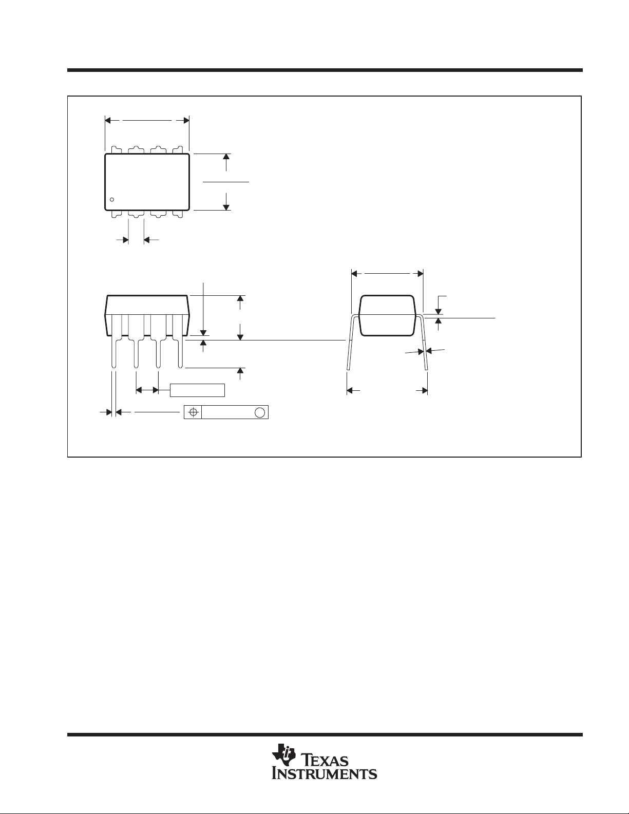
MECHANICAL DATA
MTSS001C – JANUARY 1995 – REVISED FEBRUARY 1999
PW (R-PDSO-G**) PLASTIC SMALL-OUTLINE PACKAGE
14 PINS SHOWN
0,65
1,20 MAX
14
0,30
0,19
8
4,50
4,30
PINS **
7
Seating Plane
0,15
0,05
8
1
A
DIM
14
0,10
6,60
6,20
M
0,10
0,15 NOM
0°–8°
2016
Gage Plane
24
0,25
0,75
0,50
28
A MAX
A MIN
NOTES: A. All linear dimensions are in millimeters.
B. This drawing is subject to change without notice.
C. Body dimensions do not include mold flash or protrusion not to exceed 0,15.
D. Falls within JEDEC MO-153
3,10
2,90
5,10
4,90
5,10
4,90
6,60
6,40
7,90
7,70
9,80
9,60
4040064/F 01/97
POST OFFICE BOX 655303 • DALLAS, TEXAS 75265
Page 18

Page 19
MECHANICAL DATA
MPDI001A – JANUARY 1995 – REVISED JUNE 1999
P (R-PDIP-T8) PLASTIC DUAL-IN-LINE
0.400 (10,60)
0.355 (9,02)
8
5
0.260 (6,60)
0.240 (6,10)
1
0.021 (0,53)
0.015 (0,38)
NOTES: A. All linear dimensions are in inches (millimeters).
B. This drawing is subject to change without notice.
C. Falls within JEDEC MS-001
4
0.070 (1,78) MAX
0.020 (0,51) MIN
0.200 (5,08) MAX
0.125 (3,18) MIN
0.100 (2,54)
0.010 (0,25)
Seating Plane
M
0.325 (8,26)
0.300 (7,62)
0.015 (0,38)
Gage Plane
0.010 (0,25) NOM
0.430 (10,92)
MAX
4040082/D 05/98
For the latest package information, go to http://www.ti.com/sc/docs/package/pkg_info.htm
POST OFFICE BOX 655303 • DALLAS, TEXAS 75265
Page 20

IMPORTANT NOTICE
Texas Instruments Incorporated and its subsidiaries (TI) reserve the right to make corrections, modifications, enhancements, improvements,
and other changes to its products and services at any time and to discontinue any product or service without notice. Customers should
obtain the latest relevant information before placing orders and should verify that such information is current and complete. All products are
sold subject to TI’s terms and conditions of sale supplied at the time of order acknowledgment.
TI warrants performance of its hardware products to the specifications applicable at the time of sale in accordance with TI’s standard
warranty. Testing and other quality control techniques are used to the extent TI deems necessary to support this warranty. Except where
mandated by government requirements, testing of all parameters of each product is not necessarily performed.
TI assumes no liability for applications assistance or customer product design. Customers are responsible for their products and
applications using TI components. To minimize the risks associated with customer products and applications, customers should provide
adequate design and operating safeguards.
TI does not warrant or represent that any license, either express or implied, is granted under any TI patent right, copyright, mask work right,
or other TI intellectual property right relating to any combination, machine, or process in which TI products or services are used. Information
published by TI regarding third-party products or services does not constitute a license from TI to use such products or services or a
warranty or endorsement thereof. Use of such information may require a license from a third party under the patents or other intellectual
property of the third party, or a license from TI under the patents or other intellectual property of TI.
Reproduction of TI information in TI data books or data sheets is permissible only if reproduction is without alteration and is accompanied
by all associated warranties, conditions, limitations, and notices. Reproduction of this information with alteration is an unfair and deceptive
business practice. TI is not responsible or liable for such altered documentation. Information of third parties may be subject to additional
restrictions.
Resale of TI products or services with statements different from or beyond the parameters stated by TI for that product or service voids all
express and any implied warranties for the associated TI product or service and is an unfair and deceptive business practice. TI is not
responsible or liable for any such statements.
TI products are not authorized for use in safety-critical applications (such as life support) where a failure of the TI product would reasonably
be expected to cause severe personal injury or death, unless officers of the parties have executed an agreement specifically governing
such use. Buyers represent that they have all necessary expertise in the safety and regulatory ramifications of their applications, and
acknowledge and agree that they are solely responsible for all legal, regulatory and safety-related requirements concerning their products
and any use of TI products in such safety-critical applications, notwithstanding any applications-related information or support that may be
provided by TI. Further, Buyers must fully indemnify TI and its representatives against any damages arising out of the use of TI products in
such safety-critical applications.
TI products are neither designed nor intended for use in military/aerospace applications or environments unless the TI products are
specifically designated by TI as military-grade or "enhanced plastic." Only products designated by TI as military-grade meet military
specifications. Buyers acknowledge and agree that any such use of TI products which TI has not designated as military-grade is solely at
the Buyer's risk, and that they are solely responsible for compliance with all legal and regulatory requirements in connection with such use.
TI products are neither designed nor intended for use in automotive applications or environments unless the specific TI products are
designated by TI as compliant with ISO/TS 16949 requirements. Buyers acknowledge and agree that, if they use any non-designated
products in automotive applications, TI will not be responsible for any failure to meet such requirements.
Following are URLs where you can obtain information on other Texas Instruments products and application solutions:
Products Applications
Amplifiers amplifier.ti.com Audio www.ti.com/audio
Data Converters dataconverter.ti.com Automotive www.ti.com/automotive
DSP dsp.ti.com Broadband www.ti.com/broadband
Clocks and Timers www.ti.com/clocks Digital Control www.ti.com/digitalcontrol
Interface interface.ti.com Medical www.ti.com/medical
Logic logic.ti.com Military www.ti.com/military
Power Mgmt power.ti.com Optical Networking www.ti.com/opticalnetwork
Microcontrollers microcontroller.ti.com Security www.ti.com/security
RFID www.ti-rfid.com Telephony www.ti.com/telephony
RF/IF and ZigBee® Solutions www.ti.com/lprf Video & Imaging www.ti.com/video
Mailing Address: Texas Instruments, Post Office Box 655303, Dallas, Texas 75265
Copyright © 2008, Texas Instruments Incorporated
Wireless www.ti.com/wireless
 Loading...