

PRODUCTPREVIEW
+–
V
IN
V
OUT
12V to 21V
M2
R
B
R
A
R
B
M1
L2
D2
D1
C
OUT
R
A
CPCC
PC
CZCC
ZC
RZCR
ZC
C
SS
R
RDM
R
RT
T1
T2
C
CDR
R
DMX
R
SYN
C
REF
R
PK1
R
PK2
C
ZV
R
ZV
C
PV
R
S
R
S
1
2
3
4
5
6
7
8
9
10
20
19
18
17
16
15
14
13
12
11
CAOA
CAOBPKLMT
GND
VAO
VINAC
VSENSE
CSA
CSB
RT
CDR
SS
GDB
GDA
IMO VCC
RSYNTH
VREF
DMAX
RDM
R
IMO
To CSB
To CSA
From Ixfrms
L1
UCC28070
www.ti.com
Two-Phase Interleaved CCM PFC Controller
1
FEATURES APPLICATIONS
• Interleaved Average Current-Mode PWM
Control with Inherent Current Matching
• Advanced Current Synthesizer Current
Sensing for Superior Efficiency and PF
• Highly-Linear Multiplier Output with Internal
Quantized Voltage Feed-Forward Correction
for Near-Unity PF
• Programmable Frequency (up to 300 kHz)
• Programmable Maximum Duty-Cycle Clamp
• Programmable Frequency Dithering Rate and
Magnitude for Enhanced EMI Reduction
– Magnitude: Up to 30 kHz
– Rate: Up to 30 kHz
• External Clock Synchronization Capability
• Enhanced Load and Line Transient Response
through Voltage Amplifier Output Slew-Rate
Correction
• Programmable Peak Current Limiting
• Bias-Supply UVLO, Over-Voltage Protection,
Open-Loop Detection, and PFC-Enable
Monitoring
• External PFC-Disable Interface
• Open-Circuit Protection on VSENSE and
VINAC pins
• Programmable Soft Start
• 20-Lead TSSOP Package
SLUS794 – NOVEMBER 2007
• High-Efficiency Server and Desktop Power
Supplies
• Telecom Rectifiers
DESCRIPTION
The UCC28070 is an advanced power factor
correction device that integrates two pulse-width
modulators (PWMs) operating 180 ° out of phase.
This Natural Interleaved PWM operation generates
substantial reduction in the input and output ripple
currents, and the conducted-EMI filtering becomes
easier and less expensive. A significantly improved
multiplier design provides a shared current reference
to two independent current amplifiers that ensures
matched average current mode control in both PWM
outputs while maintaining a stable, low-distortion
sinusoidal input line current.
The UCC28070 contains multiple innovations
including current synthesis and quantized voltage
feed-forward to promote performance enhancements
in PF, efficiency, THD, and transient response.
Features including frequency dithering, clock
synchronization, and slew rate enhancement further
expand the potential performance enhancements.
The UCC28070 also contains a variety of protection
features including output over-voltage detection,
programmable peak-current limit, in-rush current
detection, under-voltage lockout, and open-loop
protection.
1
Please be aware that an important notice concerning availability, standard warranty, and use in critical applications of Texas Instruments semiconductor products and disclaimers thereto appears at the end of this data sheet.
PRODUCT PREVIEW information concerns products in the
formative or design phase of development. Characteristic data and
other specifications are design goals. Texas Instruments reserves
the right to change or discontinue these products without notice.
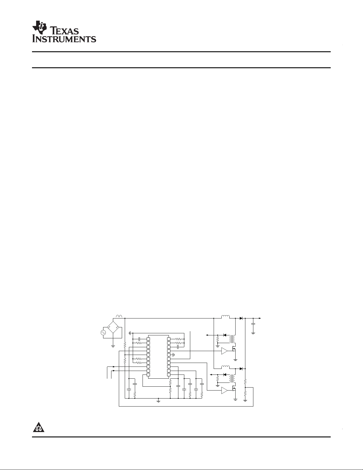
Typical Application Diagram
Copyright © 2007, Texas Instruments Incorporated
www.ti.com
PRODUCTPREVIEW
UCC28070
SLUS794 – NOVEMBER 2007
ORDERING INFORMATION
PART NUMBER PACKAGE PACKING
UCC28070PW Plastic, 20-Pin TSSOP (PW) 70-Pc. Tube
UCC28070PWR Plastic, 20-Pin TSSOP (PW) 2000-Pc. Tape and Reel
ABSOLUTE MAXIMUM RATINGS
over operating free-air temperature range (unless otherwise noted)
Supply voltage: VCC 22 V
Supply current: I
Voltage: GDA, GDB − 0.5 to VCC+0.3 V
Gate drive current – continuous: GDA, GDB +/ − 0.25
Gate drive current – pulsed: GDA, GDB +/ − 0.75
Voltage: DMAX, RDM, RT, CDR, VINAC, VSENSE, SS, VAO, IMO, CSA, CSB,
CAOA, CAOB, PKLMT, VREF
Current: RT, DMAX, RDM, RSYNTH − 0.5
Current: VREF, VAO, CAOA, CAOB, IMO 10
Operating junction temperature, T
Storage temperature, T
Lead temperature (10 seconds) 260
(1) These are stress limits. Stress beyond these limits may cause permanent damage to the device. Functional operation of the device at
these or any conditions beyond those indicated under RECOMMENDED OPERATING CONDITIONS is not implied. Exposure to
absolute maximum rated conditions for extended periods of time may affect device reliability.
(2) All voltages are with respect to GND.
(3) All currents are positive into the terminal, negative out of the terminal.
(4) In normal use, terminals GDA and GDB are connected to an external gate driver and are internally limited in output current.
VCC
STG
ELECTROSTATIC DISCHARGE (ESD) PROTECTION
Human Body Model (HBM) 2,000
Charged Device Model (CDM) 500
(1) (2) (3) (4)
PARAMETER LIMIT UNIT
20 mA
− 0.5 to +7 V
J
RATING UNIT
− 40 to +125
− 65 to +150 ° C
A
mA
V
DISSIPATION RATINGS
PACKAGE TA= 85 ° C POWER RATING
20-Pin TSSOP 125 ° C/Watt
(1) Thermal resistance is a strong function of board construction and layout. Air flow reduces thermal resistance. This number is only a
general guide.
(2) Thermal resistance calculated with a low-K methodology.
THERMAL IMPEDANCE TA= 25 ° C POWER
JUNCTION-TO-AMBIENT RATING
(1)
(2)
and
800 mW
(1)
320 mW
(1)
RECOMMENDED OPERATING CONDITIONS
over operating free-air temperature range (unless otherwise noted)
PARAMETER MIN MAX UNIT
VCC Input Voltage (from a low-impedance source) V
VREF Load Current 2 mA
VINAC Input Voltage Range 0 3
IMO Voltage Range 0 3.3 V
PKLMT, CSA, & CSB Voltage Range 0 3.7
RSYNTH Resistance (R
RDM Resistance (R
2 Submit Documentation Feedback Copyright © 2007, Texas Instruments Incorporated
) 15 750
SYN
) 30 330
RDM
Product Folder Link(s): UCC28070
+ 1 V 21 V
UVLO
k Ω

www.ti.com
PRODUCTPREVIEW
ELECTRICAL CHARACTERISTICS
over operating free-air temperature range − 40 ° C < TA< 125 ° C, TJ= TA, VCC = 12 V, GND = 0 V, R
k Ω , R
Bias Supply
VCC
V
UVLO
Linear Regulator
PFC Enable
V
EN
External PFC Disable
Oscillator
V
DMAX
and V
f
PWM
D
MAX
f
DM
f
DR
I
CDR
(1) Excessive VCC input voltage and/or current damages the device. This clamp will not protect the device from an unregulated supply. If
= R
RDM
SYN
= 100 k Ω , R
IMO
SYMBOL PARAMETER TEST CONDITIONS MIN TYP MAX UNITS
SHUNT
VCC shunt voltage
VCC current, disabled VSENSE = 0 V 7
VCC current, enabled VSENSE = 3 V (no switching) 8 TBD
VCC current, UVLO
UVLO turn-on threshold Measured at VCC (rising) 9.8 10.2 10.6
UVLO hysteresis Measured at VCC (falling) 1 V
VREF enable threshold Measured at VCC (rising) TBD 8 TBD
VREF voltage, no load I
VREF voltage, full load I
VREF voltage, over line 11 V < VCC < 20 V, I
Enable threshold Measured at VSENSE (rising) 0.65 0.75 0.85
Enable hysteresis 0.15
Disable threshold Measured at SS (falling) TBD 0.6
Hysteresis VSENSE > 0.85 V 0.15
Output phase shift Measured between GDA and GDB TBD 180 TBD Degree
,V
,
RT
RDM
Timing regulation voltages Measured at DMAX, RT, & RDM 3 V
PWM switching frequency kHz
Duty-cycle clamp TBD% 95% TBD%
Minimum programmable off-time TBD 133 TBD ns
Frequency dithering magnitude R
Change in f
PWM
Frequency dithering rate C
Rate of change in f
Dither rate current Measure at CDR (sink and source) 10 µ A
Dither disable threshold Measured at C
an unregulated supply is used, a series-connected fixed positive voltage regulator such as a UA78L15A is recommended. See the
Absolute Maximum Ratings section for the limits on VCC voltage and current.
= 16 k Ω , C
(1)
PWM
SLUS794 – NOVEMBER 2007
= 75 k Ω , R
RT
CDR
= 625 pF, C
I
VCC
= C
SS
VREF
= 0.1 µ F, C
= 1 µ F, (unless otherwise noted)
VCC
= 10 mA 21 23 25 V
VCC = 7 V 100 µ A
VCC = 9 V 4 TBD mA
= 0 mA 5.9 6 6.1
VREF
= − 2 mA 5.8 6 6.1 V
VREF
= 0 mA 5.9 6 6.1
REF
R
RT
V
RDM
R
RT
V
RDM
R
RT
V
RDM
R
RT
V
RDM
RDM
R
RDM
CDR
C
CDR
= 250 k Ω , R
= 0 V, V
= 25 k Ω , R
= 0 V, V
= 75 k Ω , R
= 0 V, V
= 25 k Ω , R
= 0 V, V
= 313 k Ω , R
= 31 k Ω , R
= 2.2 nF, R
= 0.22 nF, R
= 225 k Ω ,
DMX
= 6 V
CDR
= 22.5 k Ω ,
DMX
= 6 V
CDR
= 67.5 k Ω ,
DMX
= 6 V
CDR
= 22.5 k Ω ,
DMX
= 6 V
CDR
= 75 k Ω 2.5 3 3.5
RT
= 25 k Ω 27 30 33
RT
= 100 k Ω 3
RDM
= 100 k Ω 30
RDM
(rising) 5 TBD V
CDR
27 30 33
270 300 330
UCC28070
= 67.5
DMX
mA
V
V
kHz
Copyright © 2007, Texas Instruments Incorporated Submit Documentation Feedback 3
Product Folder Link(s): UCC28070

www.ti.com
PRODUCTPREVIEW
UCC28070
SLUS794 – NOVEMBER 2007
ELECTRICAL CHARACTERISTICS (continued)
over operating free-air temperature range − 40 ° C < TA< 125 ° C, TJ= TA, VCC = 12 V, GND = 0 V, R
k Ω , R
Clock Synchronization
V
CDR
Voltage Amplifier
g
MV
I
SRC
Soft Start
I
SS
(2) Due to the programmability of the maximum PWM switching duty cycle (D
= R
RDM
SYN
= 100 k Ω , R
SYMBOL PARAMETER TEST CONDITIONS MIN TYP MAX UNITS
SYNC enable threshold Measured at CDR (rising) 5 TBD V
SYNC propagation delay 50 TBD ns
SYNC threshold (Rising) V
SYNC threshold (Falling) V
SYNC pulses
VSENSE voltage In regulation, TA= 25 ° C 2.97 3 3.03
VSENSE voltage In regulation 2.94 3 3.06
VSENSE input bias current In regulation 250 TBD nA
VAO high voltage VSENSE = 2.9 V 4.8 5 5.2
VAO low voltage VSENSE = 3.1 V 0.05 TBD
VAO transconductance 2.8 V < VSENSE < 3.2 V, VAO = 3 V 70 µ S
VAO sink current, overdriven limit VSENSE = 3.5 V, VAO = 3 V 30
VAO source current, overdriven VSENSE = 2.5 V, VAO = 3 V, SS = 3 V − 30
VAO source current,
overdriven limit + I
Slew-rate correction threshold 92 93 95 %
Slew-rate correction hysteresis Measured at VSENSE (rising) 6 TBD mV
Slew-rate correction current − 100 µ A
Slew-rate correction enable threshold Measured at SS (rising) 4 V
VAO discharge current VSENSE = 0.5 V, VAO = 1 V 10 µ A
SS source current VSENSE = 0.9 V, SS = 1 V − 10 µ A
Adaptive source current VSENSE = 1.1 V, SS = 1 V − 1 mA
Adaptive SS disable Measured as VSENSE – SS 0 mV
SS sink current VSENSE = 0.5 V, SS = 0.2 V 0.5 0.9 mA
be reasonably (~5-10%) less than 2 x D
IMO
SRC
= 16 k Ω , C
CDR
= 625 pF, C
V
CDR
GDx (rising)
CDR
CDR
= 75 k Ω , R
= C
SS
VREF
= 0.1 µ F, C
= 1 µ F, (unless otherwise noted)
VCC
RT
= 6 V, Measured from RDM (rising) to
= 6 V, Measured at RDM (rising) 1.2 1.5
= 6 V, Measured at RDM (falling) 0.4 0.7
= 67.5
DMX
V
Positive pulse width 0.2 µ s
Maximum duty cycle
(2)
75 %
V
V
µ A
VSENSE = 2.5 V, VAO = 3 V − 130
Measured as VSENSE (falling) / VSENSE
(regulation)
Measured at VAO, in addition to VAO
source current.
), the maximum duty cycle of a synchronization pulse must
-1.
MAX
MAX
4 Submit Documentation Feedback Copyright © 2007, Texas Instruments Incorporated
Product Folder Link(s): UCC28070
www.ti.com
PRODUCTPREVIEW
ELECTRICAL CHARACTERISTICS (continued)
over operating free-air temperature range − 40 ° C < TA< 125 ° C, TJ= TA, VCC = 12 V, GND = 0 V, R
k Ω , R
Over Voltage
V
OVP
Zero-Power
V
ZPWR
Multiplier
k
MULT
I
IMO
Quantized Voltage Feed Forward
V
LVL1
V
LVL2
V
LVL3
V
LVL4
V
LVL5
V
LVL6
V
LVL7
V
LVL8
Current Amplifiers
g
MC
(3) The Level 1 threshold represents the “ zero-crossing detection ” threshold above which VINAC must rise to initiate a new input half-cycle,
= R
RDM
SYN
= 100 k Ω , R
IMO
SYMBOL PARAMETER TEST CONDITIONS MIN TYP MAX UNITS
OVP threshold 104 106 108 %
OVP hysteresis Measured at VSENSE (falling) 100 mV
OVP propagation delay TBD 0.5 µ s
Zero-power detect threshold Measured at VAO (falling) TBD 0.75
Zero-power hysteresis 0.15
Gain constant µ A
Output current: zero µ A
Level 1 threshold
(3)
Level 2 threshold 1
Level 3 threshold 1.2
Level 4 threshold 1.4
Level 5 threshold 1.65
Level 6 threshold 1.95
Level 7 threshold 2.25
Level 8 threshold 2.6
CAOx high voltage TBD 6
CAOx low voltage TBD 0.1
CAOx transconductance 100 µ S
CAOx sink current, overdriven 50
CAOx source current, overdriven − 50
Input common mode range 0 3.6 V
Input offset voltage IMO = 0 V − 1 − 3 − 5
Phase mismatch TBD 0 TBD
CAOx pull-down current VSENSE = 0.5 V, CAOx = 0.2 V 0.5 0.9 mA
and below which VINAC must fall to terminate that half-cycle.
= 16 k Ω , C
SLUS794 – NOVEMBER 2007
= 75 k Ω , R
RT
CDR
= 625 pF, C
= C
SS
VREF
= 0.1 µ F, C
= 1 µ F, (unless otherwise noted)
VCC
Measured as VSENSE (rising) / VSENSE
(regulation)
Measured between VSENSE (rising) and
GDx (falling)
VAO > 1.5 V 16 17 18
VAO = 1.2 V 15 17 19
VINAC = 0.9 VPK, VAO = 0.8 V -0.2 0 0.2
VINAC = 0 V, VAO = 5 V -0.2 0 0.2
0.6 0.7 0.8
Measured at VINAC (rising) V
Measured as Phase A ’ s input offset minus
Phase B ’ s input offset
UCC28070
= 67.5
DMX
V
V
µ A
mV
Copyright © 2007, Texas Instruments Incorporated Submit Documentation Feedback 5
Product Folder Link(s): UCC28070
www.ti.com
PRODUCTPREVIEW
GDB
SS
RT
CAOB
GND
VCC
GDA
DMAX
1
2
3
4
5
6
7
8
9
20
19
18
17
16
15
14
13
12
VAO
RDM
PKLMT
RSYNTH
CSA
VSENSE
VINAC
IMO
CDR
10
CSB VREF
CAOA
11
UCC28070
SLUS794 – NOVEMBER 2007
ELECTRICAL CHARACTERISTICS (continued)
over operating free-air temperature range − 40 ° C < TA< 125 ° C, TJ= TA, VCC = 12 V, GND = 0 V, R
k Ω , R
Current Synthesizer
V
RSYNTH
Peak Current Limit
PWM Ramp
V
RMP
In-Rush Current Detection
Gate Drive
Thermal Shutdown
= R
RDM
SYN
= 100 k Ω , R
SYMBOL PARAMETER TEST CONDITIONS MIN TYP MAX UNITS
Regulation voltage
Synthesizer disable threshold Measured at RSYNTH (rising) 5 TBD
VINAC input bias current 250 TBD nA
Peak current limit threshold PKLMT = 3.30 V, measured at CSx (rising) 3.27 3.3 3.33 V
Peak current limit propagation delay TBD 100 ns
PWM ramp amplitude 4
PWM ramp offset voltage TA= 25 ° C, R
PWM ramp offset temperature
coefficient
In-rush detection threshold Measured as VSENSE - VINAC 0
In-rush detection hyst. 20
GDA, GDB output voltage, high,
clamped
GDA, GDB output voltage, High C
GDA, GDB output voltage, Low C
Rise time GDx 1 V to 9 V, C
Fall time GDx 9 V to 1 V, C
GDA, GDB output voltage, UVLO VCC = 0 V, I
Thermal shutdown threshold 160
Thermal shutdown recovery 140
IMO
= 16 k Ω , C
= 75 k Ω , R
RT
CDR
= 625 pF, C
= C
SS
VREF
= 0.1 µ F, C
= 1 µ F, (unless otherwise noted)
VCC
VSENSE = 3 V, VINAC = 0 V 3
VSENSE = 3 V, VINAC = 2.85 V 0.15 V
Measured between CSx (rising) and GDx
(falling) edges
= 75 k Ω TBD 0.7 TBD
RT
VCC = 20 V, C
= 1 nF 10 10.5 11.5
LOAD
= 1 nF 0.2 0.3
LOAD
= 1 nF 11.5 13 15
LOAD
= 1 nF 18 30
LOAD
= 1 nF 12 25
LOAD
, I
GDA
= 2.5 mA 1.6 2 V
GDB
= 67.5
DMX
− 2 mV/ ° C
V
mV
V
ns
° C
6 Submit Documentation Feedback Copyright © 2007, Texas Instruments Incorporated
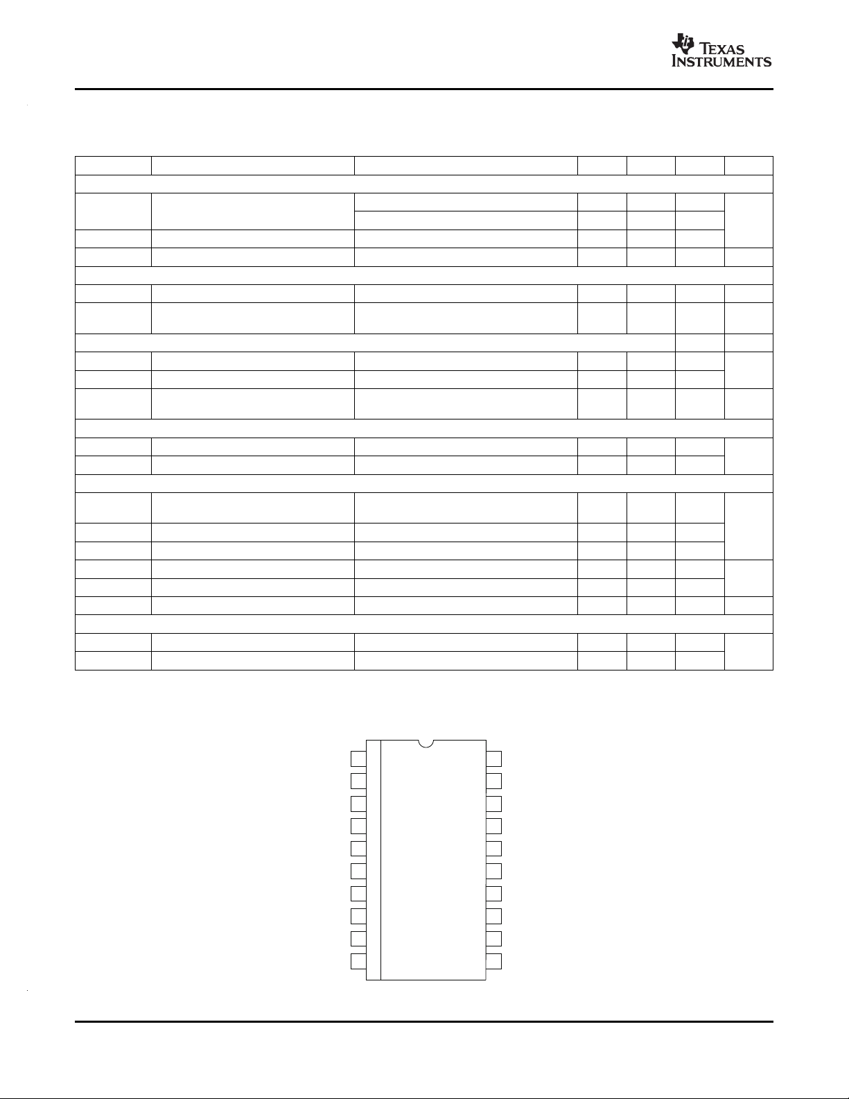
DEVICE INFORMATION
TSSOP-20 Top View, PW Package
Product Folder Link(s): UCC28070

www.ti.com
PRODUCTPREVIEW
NAME PIN # I/O DESCRIPTION
CDR 1 I
RDM
(SYNC)
VAO 3 O connected to Multiplier input and Zero-Power comparator. Connect the voltage regulation loop
VSENSE 4 I
VINAC 5 I Current Synthesis difference amplifier. Connect a resistor-divider network between VIN, VINAC,
IMO 6 O
RSYNTH 7 I
CSB 8 I
CSA 9 I
PKLMT 10 I pin to set the voltage threshold of the cycle-by-cycle peak current limiting comparators. Allows
CAOB 11 O
CAOA 12 O
VREF 13 O
GDA 14 O device suitable for driving the Phase A switching component(s). The output voltage is typically
VCC 15 I
2 I dithering is disabled (CDR > 5 V), the internal master clock will synchronize to positive edges
GND 16 I/O networks to this pin. Connect this pin to the system through a separate trace for high-current
GDB 17 O gate-drivedevice suitable for driving the Phase B switching component(s). The output voltage is
SS 18 I
RT 19 I
DMAX 20 I
UCC28070
SLUS794 – NOVEMBER 2007
TERMINAL FUNCTIONS
Dither Rate Capacitor. Frequency-dithering timing pin. An external capacitor to GND programs
the rate of oscillator dither. Connect the CDR pin to the VREF pin to disable dithering.
Dither Magnitude Resistor. Frequency-dithering magnitude and external synchronization pin. An
external resistor to GND programs the magnitude of oscillator frequency dither. When frequency
presented on the RDM pin. Connect RDM to GND when dithering is disabled and synchronization
is not desired.
Voltage Amplifier Output. Output of transconductance voltage error amplifier. Internally
compensation components between this pin and GND.
Output Voltage Sense. Internally connected to the inverting input of the transconductance
voltage error amplifier in addition to the positive terminal of the Current Synthesis difference
amplifier. Also connected to the OVP, PFC Enable, and slew-rate comparators. Connect to PFC
output with a resistor-divider network.
Scaled AC Line Input Voltage. Internally connected to the Multiplier and negative terminal of the
and GND identical to the PFC output divider network connected at VSENSE.
Multiplier Current Output. Connect a resistor between this pin and GND to set the multiplier
gain.
Current Synthesis Down-Slope Programming. Connect a resistor between this pin and GND to
set the magnitude of the current synthesizer down-slope.
Phase B Current Sense Input. During the on-time of GDB, CSB is internally connected to the
inverting input of Phase B ’ s current amplifier.
Phase A Current Sense Input. During the on-time of GDA, CSA is internally connected to the
inverting input of Phase A ’ s current amplifier.
Peak Current Limit Programming. Connect a resistor-divider network between VREF and this
adjustment for desired Δ ILB.
Phase B Current Amplifier Output. Output of phase B ’ s transconductance current amplifier.
Internally connected to the inverting input of phase B ’ s PWM comparator for trailing-edge
modulation. Connect the current regulation loop compensation components between this pin and
GND.
Phase A Current Amplifier Output. Output of phase A ’ s transconductance current amplifier.
Internally connected to the inverting input of phase A ’ s PWM comparator for trailing-edge
modulation. Connect the current regulation loop compensation components between this pin and
GND.
6-V Reference Voltage and Internal Bias Voltage. Connect a 0.1- µ F ceramic bypass capacitor
as close as possible to this pin and GND.
Phase A ’ s Gate Drive. This limited-current output is intended to connect to a separate gate-drive
clamped to 13.5 V.
Bias Voltage Input. Connect a 0.1- µ F ceramic bypass capacitor as close as possible to this pin
and GND.
Device Ground Reference. Connect all compensation and programming resistor and capacitor
noise isolation.
Phase B ’ s Gate Drive. This limited-current output is intended to connect to a separate
typically clamped to 13.5 V.
Soft-Start and External Fault Interface. Connect a capacitor to GND on this pin to set the
soft-start slew rate based on an internally-fixed 10- µ A current source. The regulation reference
voltage for VSENSE is clamped to V
conditions a 1-mA current source is present at the SS pin until the SS voltage equals the
VSENSE voltage. Pulling the SS pin below 0.6 V immediately disables both GDA and GDB
outputs.
Timing Resistor. Oscillator frequency programming pin. A resistor to GND sets the running
frequency of the internal oscillator.
Maximum Duty-Cycle Resistor. Maximum PWM duty-cycle programming pin. A resistor to GND
sets the PWM maximum duty-cycle based on the ratio of R
until V
SS
exceeds 3 V. Upon recovery from certain fault
SS
/R
.
DMX
RT
Copyright © 2007, Texas Instruments Incorporated Submit Documentation Feedback 7
Product Folder Link(s): UCC28070
www.ti.com
PRODUCTPREVIEW
14
GDA
VCC
17
GDB
+
S Q
QR
PWM1
+
S Q
QR
PWM2
CLKB
OffB
IpeakB
+
+
12
CAOA
11
CAOB
Driver
Driver
8CSB
9
CSA
10
7
CA2
CA1
CLKA
OffA
IpeakA
Gm Amp
Gm Amp
+
+
IpeakA
IpeakB
GND
PKLMT
RSYNTH
Current
Synthesizer
VINAC
VSENSE
OutA
OutB
GND
Fault
(Clamped at 13.5V)
VCC
(Clamped at 13.5V)
Fault
VSENSE
3 VAO
18 SS
4
3V
250nA
ISS
Mult.
x
x
/
VA
Gm Amp
+
+
+
2.8V
VINAC5
6 IMO
Slew Rate
Correction
10uA
100uA
5V
250nA
ReStart
+
SS
4V
I
IMO
=
V
VINAC
* (V
VAO
– 1)
K
VFF
* 17uA
Voltage
Feed-
Forward
K
VFF
ReStart
10uA
+
5V
Disable
ReStart
Ext. Disable
1mA
+
Adaptive SS
Control
Logic
20
DMAX
2
RDM/
SYNC
CLKA
CLKB
OffA
OffB
SYNC
Logic
1
CDR
19
RT
Oscillator w/
Freq. Dither
+
5V
SYNC
Enable
Dither
Disable
15VCC
+
10.2V
16GND
13VREF
6V
Linear
Regulator
+
8V
EN
23V
9.2V
S Q
QR
+
0.75V
ReStart
C
o
ThermSD
160 On
140 Off
0.60V
VSENSE
+
3.18V
+
ZeroPwr 0.75V
VSENSE
SS
0.75V
+
VAO
OVP
Ext. Disable
0.60V
3.08V
0.90V
VINAC
In-Rush
20mV Hys.
20mV
+
Fault
UVLO
UCC28070
SLUS794 – NOVEMBER 2007
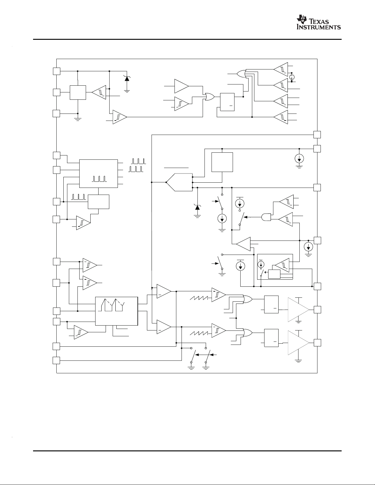
Functional Block Diagram
8 Submit Documentation Feedback Copyright © 2007, Texas Instruments Incorporated
Product Folder Link(s): UCC28070

www.ti.com
PRODUCTPREVIEW
( )
( )
7500
RT
PWM
R k
f kHz
W =
( )
2 1
DMX RT MAX
R R D= ´ ´ -
UCC28070
SLUS794 – NOVEMBER 2007
APPLICATION INFORMATION
THEORY OF OPERATION
Natural Interleaving
One of the main benefits from the natural interleaving of phases is significant reductions in the high-frequency
ripple components of both the input current and the current into the output capacitor of the PFC pre-regulator.
Compared to that of a single-phase PFC stage of equal power, the reduced ripple on the input current eases the
burden of filtering conducted-EMI noise and helps reduce the EMI filter and C
high-frequency ripple current into the PFC output capacitor, C
, helps to reduce its size and cost. Furthermore,
OUT
with reduced ripple and average current in each phase, the boost inductor size can be smaller than in a
single-phase design [1].
Ripple current reduction due to interleaving is often referred to as “ ripple cancellation ” , but strictly speaking, the
peak-to-peak ripple is completely cancelled only at 50% duty-cycle in a 2-phase system. At duty-cycles other
than 50%, ripple reduction occurs in the form of partial cancellation due to the superposition of the individual
phase currents. Nevertheless, compared to the ripple currents of an equivalent single-phase PFC pre-regulator,
those of a 2-phase naturally-interleaved design are extraordinarily smaller [1]. Independent of ripple cancellation,
the frequency of the naturally-interleaved ripple, at both the input and output, is 2 x f
On the input, natural interleaving reduces the peak-to-peak ripple amplitude to 1/2 or less of the ripple amplitude
of the equivalent single-phase current.
On the output, Natural Interleaving reduces the rms value of the PFC-generated ripple current in the output
capacitor by a factor of slightly more than √ 2, for PWM duty-cycles > 50% as derived from following Erickson ’ s
method [2].
sizes. Additionally, reduced
IN
.
PWM
Programming the PWM Frequency and Maximum Duty-Cycle Clamp
The PWM frequency and maximum duty-cycle clamps for both GDx outputs of the UCC28070 are set through
the selection of the resistors connected to the RT and DMAX pins, respectively. The selection of the RT resistor
(R
) directly sets the PWM frequency (f
RT
Once R
where D
has been determined, the D
RT
is the desired maximum PWM duty-cycle.
MAX
MAX
PWM
).
resistor (R
) may be derived.
DMX
Copyright © 2007, Texas Instruments Incorporated Submit Documentation Feedback 9
Product Folder Link(s): UCC28070

www.ti.com
PRODUCTPREVIEW
( )
( )
937 5
RDM
DM
.
R k
f kHz
W =
( ) ( )
66 7
RDM
CDR
DR
R
C pF . k / kHz
f
æ ö
= ´ W
ç ÷
è ø
UCC28070
SLUS794 – NOVEMBER 2007
Frequency Dithering (Magnitude and Rate)
Frequency dithering refers to modulating the switching frequency to achieve a reduction in conducted-EMI noise
beyond the capability of the line filter alone. The UCC28070 implements a triangular modulation method which
results in equal time spent at every point along the switching frequency range. This total range from minimum to
maximum frequency is defined as the dither magnitude, and is centered around the nominal switching frequency
f
set with R
PWM
frequency range of 100 kHz ± 10 kHz. Furthermore, the programmed duty-cycle clamp set by R
constant at the programmed value across the entire range of the frequency dithering.
The rate at which f
example, a dither rate of 1 kHz would linearly modulate the nominal frequency from 110 kHz to 90 kHz to 110
kHz once every millisecond. A good initial design target for dither magnitude is ± 10% of f
components can tolerate such a spread in f
compromise between EMI reduction, component tolerances, and loop stability.
The desired dither magnitude is set by a resistor from the RDM pin to GND, of value calculated by the following
equation:
. For example, a dither magnitude of 20 kHz on a nominal f
RT
traverses from one extreme to the other and back again is defined as the dither rate. For
PWM
. The designer can then iterate around there to find the best
PWM
of 100 kHz results in a
PWM
PWM
. Most boost
remains
DMX
Once the value of R
GND, of value calculated by the following equation:
Frequency dithering may be fully disabled by forcing the CDR pin > 5 V or by connecting it to VREF (6 V) and
connecting the RDM pin directly to GND. (If populated, the relatively high impedance of the RDM resistor may
allow system switching noise to couple in and interfere with the controller timing functions if not bypassed with a
low impedance path when dithering is disabled.)
If an external frequency source is used to synchronize f
frequency source must provide the dither magnitude and rate functions as the internal dither circuitry is disabled
to prevent undesired performance during synchronization. (See SubSec2 0.1 section for more details.)
is determined, the desired dither rate may be set by a capacitor from the CDR pin to
RDM
and frequency dithering is desired, the external
PWM
10 Submit Documentation Feedback Copyright © 2007, Texas Instruments Incorporated
Product Folder Link(s): UCC28070

www.ti.com
PRODUCTPREVIEW
2
SYNC
PWM
f
f =
( )
( )
15000
'
RT
SYNC
R k
f kHz
W =
( ) ( )
2 1
'
DM X RT MAX
R k R DW = ´ ´ -
( )
( )
15000
1 1
RT
SYNC
R k .
f kHz
W = ´
( )
0 9 2 1
SYN(max D ) MAX
f . D£ ´ ´ -
UCC28070
SLUS794 – NOVEMBER 2007
External Clock Synchronization
The UCC28070 has also been designed to be easily synchronized to almost any external frequency source. By
disabling frequency dithering (pulling CDR > 5 V), the UCC28070 ’ s SYNC circuitry is enabled permitting the
internal oscillator to be synchronized with pulses presented on the RDM pin. In order to ensure a precise 180
degree phase shift is maintained between the GDA and GDB outputs, the frequency (f
presented at the RDM pin needs to be at twice the desired f
is desired, the f
SYNC
should be 200 kHz.
In order to ensure the internal oscillator does not interfere with the SYNC function, R
internal oscillator frequency at least 10% below the f
reduced by a factor equivalent to the scaled R
R
. Adjustments to the current loops should be made accordingly.
RT
due to a direct correlation between the PWM ramp current and
RT
. It must be noted that the PWM modulator gain will be
SYNC
The maximum duty-cycle clamp programmability is still maintained via the selection of R
. For example, if a 100-kHz switching frequency
PWM
should be sized to set the
RT
DMX
and third equations below.
SYNC
based on the second
) of the pulses
When external synchronization is used, a propagation delay of approximately 50 ns to
100 ns exists between internal timing circuits and the SYNC signal ’ s rising edge,
which may result in reduced off-time at the highest of switching frequencies.
Therefore, R
DMX
compensate. At lower SYNC frequencies, this delay becomes an insignificant fraction
of the PWM period, and can be neglected.
NOTE:
should be adjusted downward slightly by (T
-0.1 µ s)/T
SYNC
to
SYNC
Copyright © 2007, Texas Instruments Incorporated Submit Documentation Feedback 11
Product Folder Link(s): UCC28070

www.ti.com
PRODUCTPREVIEW
( )
B
R
A B
R
k
R R=+
UCC28070
SLUS794 – NOVEMBER 2007
Multi-phase Operation
External synchronization also facilitates using more than 2 phases for interleaving. Multiple UCC28070s can
easily be paralleled to add an even number of additional phases for higher-power applications. With appropriate
phase-shifting of the synchronization signals, even more input and output ripple current cancellation can be
obtained. (An odd number of phases can be accommodated if desired, but the ripple cancellation would not be
optimal.) For 4-, 6-, or any 2 x n-phases (where n = the number of UCC28070 controllers), each controller should
receive a SYNC signal which is 360/n degrees out of phase with each other. For a 4-phase application
interleaving with two controllers, SYNC1 should be 180 ° out of phase with SYNC2 for optimal ripple cancellation.
Similarly for a 6-phase system, SYNC1, SYNC2, and SYNC3 should be 120 ° out of phase with each other for
optimal ripple cancellation.
In a multi-phase interleaved system, each current loop is independent and treated separately, however there is
only one common voltage loop. To maintain a single control loop, all VSENSE, VINAC, SS, IMO and VAO
signals are paralleled, respectively between the n controllers. Where current-source outputs are combined (SS,
IMO, VAO), the calculated load impedances must be adjusted by 1/n to maintain the same performance as with
a single controller.
Figure 20 illustrates the paralleling of two controllers for a 4-phase 90 ° -interleaved PFC system.
VSENSE and VINAC Resistor Configuration
The primary purpose of the VSENSE input is to provide the voltage feedback from the output to the voltage
control loop. Thus, a traditional resistor-divider network needs to be sized and connected between the output
capacitor and the VSENSE pin to set the desired output voltage based on the 3-V regulation voltage on
VSENSE.
A unique aspect of the UCC28070 is the need to place the same resistor-divider network on the V
inductor to the VINAC pin. This provides the scaled input voltage monitoring needed for the linear multiplier and
current synthesizer circuitry. It is not required that the actual resistance of the VINAC network be identical to the
VSENSE network, but it is necessary that the attenuation (k
proper PFC operation.
side of the
IN
) of the two divider networks be equivalent for
R
In noisy environments, it may be beneficial for small filter capacitors to be applied to the VSENSE and VINAC
inputs to avoid the destabilizing effects of excessive noise on these inputs. If applied, the RC time-constant
should not exceed 100 µ s on the VSENSE input to avoid significant delay in the output transient response. The
RC time-constant should also not exceed 100 µ s on the VINAC input to avoid degrading of the wave-shape
zero-crossings. Usually, a time constant of 3/f
is adequate to filter out typical noise on VSENSE and VINAC.
PWM
Some design and test iteration may be required to find the optimal amount of filtering required in a particular
application.
VSENSE and VINAC Open Circuit Protection
Both the VSENSE and VINAC pins have been designed with an internal 250-nA current sink to ensure that in the
event of an open circuit at either pin, the voltage is not left undefined, and the UCC28070 remains in a “ safe ”
operating mode.
12 Submit Documentation Feedback Copyright © 2007, Texas Instruments Incorporated
Product Folder Link(s): UCC28070

www.ti.com
PRODUCTPREVIEW
+–
VIN
12V to 21V
M4
R
B
M3
L4
L3
D4
D3
C
OUT
R
A
C
SS
RRT2
T3
T4
R
DMX
2
C
REF
RS3
RS4
1
2
3
4
5
6
7
8
9
10
20
19
18
17
16
15
14
13
12
11
CAOA
CAOBPKLMT
GND
VAO
VINAC
VSEN SE
CSA
CSB
RT
CDR
SS
GDB
GDA
IMO V CC
RSYN TH
VREF
DMAX
RDM
R
IMO
To CSA2
To CSB2
12V to 21V
M2
M1
L2
L1
C
PC
C
ZC
R
ZC
R
ZC
RRT1
T1
T2
R
DMX
1
R
PK1
R
PK2
RS1
RS2
1
2
3
4
5
6
7
8
9
10
20
19
18
17
16
15
14
13
12
11
CAOA
CAOBPKLMT
GND
VAO
VINAC
VSEN SE
CSA
CSB
RT
CDR
SS
GDB
GDA
IMO V CC
RSYN TH
VREF
DMAX
RDM
To CSB1
To CSA1
R
B
R
A
D2
D1
VREF1
From Ixfrms
R
SYN
1
VREF1
Vin
From Ixfrms
VREF2
Synchronized
Clock s
w/ 180
o
Phase Shift
CSB1
CSA1
CSB2
CSA2
R
SYN
2
R
ZC
R
ZC
C
ZC
C
ZC
C
ZC
C
PC
C
PC
C
PC
C
REF
C
ZV
R
ZV
C
PV
V
OUT
UCC28070
SLUS794 – NOVEMBER 2007
Figure 20. Functional Four-Phase Application Schematic Using Two UCC28070
Copyright © 2007, Texas Instruments Incorporated Submit Documentation Feedback 13
Product Folder Link(s): UCC28070

www.ti.com
PRODUCTPREVIEW
Waveform at
CSx input
Synthesized
down- slope
Current Synthesizer
output to CA
( )
( )
( )
( )
10
CT B R
SYN
S
N L H k
R k
R
m´ ´ ´
W =
W
UCC28070
SLUS794 – NOVEMBER 2007
Current Synthesizer
One of the most prominent innovations in the UCC28070 design is the current synthesizer circuitry that
synchronously monitors the instantaneous inductor current through a combination of on-time sampling and
off-time down-slope emulation.
During the on-time of the GDA and GDB outputs, the inductor current is recorded at the CSA and CSB pins
respectively via the current transformer network in each output phase. Meanwhile, the continuous monitoring of
the input and output voltage via the VINAC and VSENSE pins permits the UCC28070 to internally recreate the
inductor current ’ s down-slope during each output ’ s respective off-time. Through the selection of the RSYNTH
resistor (R
range of inductances expected across the wide array of applications.
), based on the equation below, the internal circuitry may be adjusted to accommodate the wide
SYN
Variables
• LB= Nominal Boost Inductance ( µ H),
• R
= Sense Resistor ( Ω ),
S
• N
• kR= RB/(R
= Current-sense Transformer turns ratio,
CT
+R
) = the resistor-divider attenuation at the VSENSE and VINAC pins.
A
B
Figure 21. Inductor Current ’ s Down Slope
14 Submit Documentation Feedback Copyright © 2007, Texas Instruments Incorporated
Product Folder Link(s): UCC28070

www.ti.com
PRODUCTPREVIEW
CSx
+
IPEAKx
10
PKLMT
Current
Synthesizer
Externally Programmable Peak
Current Limit level (PKLMT)
3V Average Current-sense
Signal Range, plus Ripple
To Current
Amplifier
To Gate-Drive
Shut-down
DI
UCC28070
SLUS794 – NOVEMBER 2007
Programmable Peak Current Limit
The UCC28070 has been designed with a programmable cycle-by-cycle peak current limit dedicated to disabling
either GDA or GDB output whenever the corresponding current-sense input (CSA or CSB respectively) rises
above the voltage established on the PKLMT pin. Once an output has been disabled via the detection of peak
current limit, the output remains disabled until the next clock cycle initiates a new PWM period. The programming
range of the PKLMT voltage extends to upwards of 4 V to permit the full utilization of the 3-V average current
sense signal range.
A resistor-divider network from VREF to GND can easily program the peak current limit voltage on PKLMT,
provided the total current out of VREF is less than 2 mA to avoid drooping of the 6-V VREF voltage. A load of
less than 0.5 mA is suggested, but if the resistance on PKLMT is very high, a small filter capacitor on PKLMT is
recommended to avoid operational problems in high-noise environments.
Copyright © 2007, Texas Instruments Incorporated Submit Documentation Feedback 15
Figure 22. Externally Programmable Peak Current Limit
Product Folder Link(s): UCC28070

www.ti.com
PRODUCTPREVIEW
UCC28070
SLUS794 – NOVEMBER 2007
Linear Multiplier
The multiplier of the UCC28070 generates a reference current which represents the desired wave shape and
proportional amplitude of the ac input current. This current is converted to a reference voltage signal by the R
resistor, which is scaled in value to match the voltage of the current-sense signals. The instantaneous multiplier
current is dependent upon the rectified, scaled input voltage V
The V
1. The overall wave-shape of the input voltage (typically sinusoidal),
2. the instantaneous input voltage magnitude at any point in the line cycle,
3. and the rms level of the input voltage.
The V
A major innovation in the UCC28070 multiplier architecture is the internal quantized V
circuitry, which eliminates the requirement for external filtering of the VINAC signal and the subsequent slow
response to transient line variations. A unique circuit algorithm detects the transition of the peak of V
through seven thresholds and generates an equivalent VFF level centered within the eight Q
boundaries of the ranges expand with increasing V
between levels. These eight Q
V
RMS
A great benefit of the Q
multiplier output, unlike an externally-filtered VINAC signal which unavoidably contains 2nd-harmonic distortion
components. Furthermore, the Q
changes in input rms voltage so that disturbances transmitted to the PFC output are minimized. 5% hysteresis in
the level thresholds help avoid “ chattering ” between Q
threshold or containing mild ringing or distortion. The Q
sinusoidal, and relies on detecting zero-crossings to adjust Q
Zero-crossings are defined as V
Table 1 reflects the relationship between the various VINAC peak voltages and the corresponding k
the multiplier equation.
signal conveys three pieces of information to the multiplier:
VINAC
signal represents the total output power of the PFC pre-regulator.
VAO
.
VFF
levels are spaced to accommodate the full “ universal ” line range of 85 V-265
VFF
architecture is that the fixed k
algorithm allows for rapid response to both increasing and decreasing
VFF
falling below 0.7 V for at least 50 µ s typically.
VINAC
and the voltage-error amplifier output V
VINAC
feed-forward (Q
RMS
to maintain an approximately equal-percentage delta
IN
factors eliminate any contribution to distortion of the
VFF
levels for V
VFF
architecture requires that the input voltage be largely
VFF
downward on decreasing input voltage.
VFF
voltage peaks near a particular
VINAC
IMO
.
VAO
)
VFF
ranges. The
VFF
VFF
VINAC
terms for
Table 1. VINAC Peak Voltages
LEVEL V
8 2.60 V ≤ V
7 2.25 V ≤ V
6 1.95 V ≤ V
5 1.65 V ≤ V
4 1.40 V ≤ V
3 1.20 V ≤ V
2 1.00 V ≤ V
1 V
(1) The VINpeak voltage boundary values listed above are calculated based on a 400-V PFC output voltage and the use of a matched
resistor-divider network (k
to be higher or lower than 400 V, kR= 3 V/V
= 3 V/400 V = 0.0075) on VINAC and VSENSE (as required for current synthesis). When V
R
PEAK VOLTAGE k
VINAC
VINAC(pk)
VINAC(pk)
VINAC(pk)
VINAC(pk)
VINAC(pk)
VINAC(pk)
VINAC(pk)
VINAC(pk)
OUT
< 2.60 V 2.922 300 V to 345 V
< 2.25 V 2.199 260 V to 300 V
< 1.95 V 1.604 220 V to 260 V
< 1.65 V 1.156 187 V to 220 V
< 1.40 V 0.839 160 V to 187 V
< 1.20 V 0.600 133 V to 160 V
≤ 1.00 V 0.398 < 133 V
, and the VINpeak voltage boundary values for each Q
(V2) VINPEAK VOLTAGE
VFF
3.857 > 345 V
level adjust to V
VFF
(1)
is designed
OUT
/kR.
VINAC(pk)
16 Submit Documentation Feedback Copyright © 2007, Texas Instruments Incorporated
Product Folder Link(s): UCC28070

www.ti.com
PRODUCTPREVIEW
( ) ( )
17 1
VINAC VAO
IMO
VFF
A V V
I
k
m ´ ´ -
=
1 10
OUT (max)
IN (max)
. P
P
h
´
=
1 414
73
IN (max)
IN ( rms ) IN ( pk ) IN ( rms )
RMS
P
I , I . I
V
= = ´Thus and
UCC28070
SLUS794 – NOVEMBER 2007
The multiplier output current I
Because the k
downwards when VINAC
value represents the scaled V
VFF
pk
the difference. This is automatically accomplished by the voltage loop control when V
for any line and load condition can thus be determined by the equation
IMO
2
at the center of a level, V
RMS
is either lower or higher than the center of the Q
will adjust slightly upwards or
VAO
voltage range to compensate for
VFF
varies, both within a level
IN
and after a transition between levels.
The output of the voltage-error amplifier VAO is clamped at 5.0 V, which represents the maximum PFC output
power. This value is used to calculate the maximum reference current at the IMO pin, and sets a limit for the
maximum input power allowed (and, as a consequence, limits maximum output power).
Unlike a continuous V
Q
levels permit a variation in maximum input power within limited boundaries as the input V
VFF
situation, where maximum input power is a fixed power at any V
FF
input, the discrete
RMS
varies within
RMS
each level.
The lowest maximum power limit occurs at the VINAC voltage of 0.76 V, while the highest maximum power limit
occurs at the increasing threshold from level-1 to level-2. This pattern repeats at every level transition threshold,
keeping in mind that decreasing thresholds are 95% of the increasing threshold values. Below VINAC = 0.76 V,
P
is always less than P
IN
, falling linearly to zero with decreasing input voltage.
IN(max)
For example, to design for the lowest maximum power allowable, determine the maximum steady-state (average)
output power required of the PFC pre-regulator and add some additional percentage to account for line drop-out
recovery power (to recharge C
while full load power is drawn) such as 10% or 20% of P
OUT
OUT(max)
. Then apply
the expected efficiency factor to find the lowest maximum input power allowable:
At the P
design threshold, V
IN(max)
2-V bridge-rectifier drop) for a nominal 400-V output system.
= 0.76 V, hence Q
VINAC
= 0.398 and input V
VFF
= 73 V
AC
RMS
(accounting for
Copyright © 2007, Texas Instruments Incorporated Submit Documentation Feedback 17
Product Folder Link(s): UCC28070

www.ti.com
PRODUCTPREVIEW
( )( )
0 76 5 1
17 130
0 398
IMO(max)
. V V V
I A A
.
m m
-
= ´ =
1
2
S
IMO IMO(max) IN ( pk )
CT
R
R I I
N
æ ö
´ = ´ ´
ç ÷
è ø
( )
1
2
IN ( pk ) S
IMO
CT IMO(max)
I R
R
N I
æ ö
æ ö
´ ´
ç ÷
ç ÷
è ø
è ø
=
´
( )( )
1 2
1 0 5 1
17 171
0 398
IMO( L L )
. V V V
I A A
.
m m
-
-
= ´ =
UCC28070
SLUS794 – NOVEMBER 2007
This I
voltage. Each inductor current is detected and scaled by a current-sense transformer (CT). Assuming equal
currents through each interleaved phase, the signal voltage at each current sense input pin (CSA and CSB) is
developed across a sense resistor selected to generate ~3 V based on (1/2) x I
burden current sense resistor and N
I
is then calculated at that same lowest maximum-power point, as
IMO
R
IMO
Therefore:
At the increasing side of the level-1 to level-2 threshold, it should be noted that the IMO current would allow
much higher input currents at low-line:
value represents the combined average current through the boost inductors at the peak of the line
IN(pk)
x RS/N
IN(pk)
is selected such that:
is the CT turns-ratio.
CT
, where R
CT
is the
S
However, this current may easily be limited by the programmable peak current limiting (PKLMT) feature of the
UCC28070 if required by the power stage design.
The same procedure can be used to find the lowest and highest input power limits at each of the Q
transition thresholds. At higher line voltages, where the average current with inductor ripple is traditionally below
the PKLMT threshold, the full variation of maximum input power will be seen, but the input currents will inherently
be below the maximum acceptable current levels of the power stage.
The performance of the multiplier in the UCC28070 has been significantly enhanced when compared to previous
generation PFC controllers, with high linearity and accuracy over most of the input ranges. The accuracy is at its
worst as V
IMO reference current to a greater degree.
Enhanced Transient Response (VA Slew-Rate Correction)
Due to the low voltage loop bandwidth required to maintain proper PFC and ignore the slight 120-Hz ripple on
the output, the response of ordinary controllers to input voltage and load transients will also be slow. However,
the Q
VFF
needed within a Q
the UCC28070 has been designed to improve its transient response by pulling up on the output of the voltage
amplifier (VAO) with an additional 100 µ A of current in the event the VSENSE voltage drops below 93% of
regulation (2.79 V). During a soft-start cycle, when VSENSE is ramping up from the 0.75-V PFC Enable
threshold, the 100- µ A correction current source is disabled to ensure the gradual and controlled ramping of
output voltage and current during a soft start.
approaches 1 V because the error of the (V
VAO
function effectively handles the line transient response with the exception of any minor adjustments
level. Load transients on the other hand can only be handled by the voltage loop, therefore,
VFF
-1) subtraction increases and begins to distort the
VAO
level
VFF
18 Submit Documentation Feedback Copyright © 2007, Texas Instruments Incorporated
Product Folder Link(s): UCC28070

www.ti.com
PRODUCTPREVIEW
UCC28070
SLUS794 – NOVEMBER 2007
Voltage Biasing (VCC and VREF)
The UCC28070 operates within a VCC bias supply range of 10 V to 21 V. An Under-Voltage Lock-Out (UVLO)
threshold prevents the PFC from activating until VCC > 10.2 V, and 1 V of hysteresis assures reliable start-up
from a possibly low-compliance bias source. An internal 23-V zener-like clamp on VCC is intended only to protect
the device from brief energy-limited surges from the bias supply, and should NOT be used as a regulator with a
current-limited source.
At minimum, a 0.1- µ F ceramic bypass capacitor must be applied from VCC to GND close to the device pins to
provide local filtering of the bias supply. Larger values may be required depending on I
magnitudes and durations to minimize ripple voltage on VCC.
In order to provide a smooth transition out of UVLO and to make the 6-V voltage reference available as early as
possible, the VREF output is enabled when VCC exceeds 8 V typically.
The VREF circuitry is designed to provide the biasing of all internal control circuits and for limited use externally.
At minimum, a 22-nF ceramic bypass capacitor must be applied from VREF to GND close to the device pins to
ensure stability of the circuit. External load current on VREF should be limited to less than 2 mA, or degraded
regulation may result.
PFC Enable and Disable
The UCC28070 contains two independent circuits dedicated to disabling the GDx outputs based on the biasing
conditions of the VSENSE or SS pins. The first circuit which monitors the V
, is the traditional PFC Enable
VSENSE
that holds off soft-start and the overall PFC function until the output has pre-charged to ~25%. Prior to V
reaching 0.75 V, almost all of the internal circuitry is disabled. Once V
VSENSE
reaches 0.75 V and VAO < 0.75 V,
the oscillator, multiplier, and current synthesizer are enabled and the SS circuitry begins to ramp up the voltage
on the SS pin. The second circuit provides an external interface to emulate an internal fault condition to disable
the GDx output without fully disabling the voltage loop and multiplier. By externally pulling the SS pin below 0.6
V, the GDx outputs are immediately disabled and held low. Assuming no other fault conditions are present,
normal PWM operation resumes when the external SS pull-down is released. It must be noted that the external
pull-down needs to be sized large enough to override the internal 1-mA adaptive SS pull-up once the SS voltage
falls below the disable threshold. It is recommended that a MOSFET with less than 100- Ω R
used to ensure the SS pin is held adequately below the disable threshold.
DS(on)
peak current
CC
resistance be
VSENSE
Copyright © 2007, Texas Instruments Incorporated Submit Documentation Feedback 19
Product Folder Link(s): UCC28070

www.ti.com
PRODUCTPREVIEW
2 25
10
SS SS
. V
t C
Am
æ ö
= ´
ç ÷
è ø
0
3
10
VSENSE
SS SS
V V
t C
Am
æ ö
-
= ´
ç ÷
è ø
V
SS
V
VSENSE
VSSif no adaptive current
Time (s)
(V)
PFC externally
disabled due to
AC-line drop-out
AC-Line recovers
and SS pin released
Reduced delay to regulation
UCC28070
SLUS794 – NOVEMBER 2007
Adaptive Soft Start
In order to maintain a controlled power up, the UCC28070 has been designed with an adaptive soft-start function
that overrides the internal reference voltage with a controlled voltage ramp during power up. On initial power up,
once V
VSENSE
the 1-mA adaptive soft-start current source is activated. This 1-mA pull-up almost immediately pulls the SS pin to
0.75 V (V
SS pin has reached the voltage on VSENSE, the 10- µ A soft-start current (I
selection of the soft-start capacitor (C
the equation below.
Often, a system restart is desired following a brief shut-down. In such a case, VSENSE may still have substantial
voltage if V
charging C
voltage sag, the adaptive soft start uses a 1-mA current source to rapidly charge C
the 10- µ A source controls the V
follows:
exceeds the 0.75-V enable threshold (V
) to bypass the initial 25% of dead time during a traditional 0 V to Vregulation SS ramp. Once the
VSENSE
), the effective soft-start time (t
SS
has not fully discharged or if high line has peak charged C
OUT
from 0 V up to the pre-charged V
SS
accent to the desired soft-start ramp rate. In such a case, tSSis estimated as
SS
VSENSE
), the internal pull down on the SS pin is released, and
EN
) takes over. Thus, through the
SS
) may be easily programmed based on
SS
. To eliminate the delay caused by
OUT
with only the 10- µ A current source and any further output
to V
SS
VSENSE
, after which time
where V
VSENSE0
is the voltage at VSENSE at the moment a soft start or restart is initiated.
Figure 23. Soft-Start Ramp Rate
20 Submit Documentation Feedback Copyright © 2007, Texas Instruments Incorporated
Product Folder Link(s): UCC28070

www.ti.com
PRODUCTPREVIEW
UCC28070
SLUS794 – NOVEMBER 2007
PFC Start-Up Hold Off
An additional feature designed into the UCC28070 is the “ Start-Up Hold Off ” logic that prevents the device from
initiating a soft-start cycle until the VAO is below the zero-power threshold (0.75 V). This feature ensures that the
SS cycle will initiate from zero-power and zero duty-cycle while preventing the potential for any significant inrush
currents due to stored charge in the VAO compensation network.
Output Over-Voltage Protection (OVP)
Because of the high voltage output and a limited design margin on the output capacitor, output over-voltage
protection is essential for PFC circuits. The UCC28070 implements OVP through the continuous monitoring of
the VSENSE voltage. In the event V
VSENSE
immediately disabled to prevent the output voltage from reaching excessive levels. Meanwhile the CAOx outputs
are pulled low in order to ensure a controlled recovery starting from 0% duty-cycle after an OVP fault is released.
Once the V
VSENSE
voltage has dropped below 3.08 V, the PWM operation resumes normal operation.
Zero-Power Detection
In order to prevent undesired performance under no-load and near no-load conditions, the UCC28070
zero-power detection comparator is designed to disable both GDA and GDB output in the event the VAO voltage
falls below 0.75 V. The 150 mV of hysteresis ensures that the output remains disabled until the VAO has nearly
risen back into the linear range of the multiplier (VAO ≥ 0.9 V).
Thermal Shutdown
In order to protect the power supplies from silicon failures at excessive temperatures, the UCC28070 has an
internal temperature-sensing comparator that shuts down nearly all of the internal circuitry, and disables the GDA
and GDB outputs, if the die temperature rises above 160 ° C. Once the die temperature falls below 140 ° C, the
device brings the outputs up through a typical soft start.
rises above 106% of regulation (3.18 V), the GDx outputs are
Copyright © 2007, Texas Instruments Incorporated Submit Documentation Feedback 21
Product Folder Link(s): UCC28070

www.ti.com
PRODUCTPREVIEW
UCC28070
SLUS794 – NOVEMBER 2007
Advanced Design Techniques
Current Loop Feedback Configuration
(Sizing of the Current Transformer Turns Ratio and Sense Resistor (R
A current-sense transformer (C
avoiding significant losses in the sensing resistor. For average current-mode control, the entire inductor current
waveform is required; however low-frequency CTs are obviously impracticable. Normally, two high-frequency
CTs are used, one in the switching leg to obtain the up-slope current and one in the diode leg to obtain the
down-slope current. These two current signals are summed together to form the entire inductor current, but this
is not the case for the UCC28070.
A major advantage of the UCC28070 design is the current synthesis function, which internally recreates the
inductor current down-slope during the switching period off-time. This eliminates the need for the diode-leg CT in
each phase, significantly reducing space, cost and complexity. A single resistor programs the synthesizer down
slope, as previously discussed in SubSec2 0.2 .
A number of trade-offs must be made in the selection of the CT. Various internal and external factors influence
the size, cost, performance, and distortion contribution of the CT.
These factors include, but are not limited to:
• Turns-ratio (N
• Magnetizing inductance (L
• Leakage inductance (L
• Volt-microsecond product (V µ s)
• Distributed capacitance (C
• Series resistance (R
• External diode drop (V
• External current sense resistor (R
• External reset network
Traditionally, the turns-ratio and the current sense resistor are selected first. Some iterations may be needed to
refine the selection once the other considerations are included.
)
CT
SER
)
S
) is typically used in high-power applications to sense inductor current while
T
)
M
)
LK
)
d
)
)
D
)
S
22 Submit Documentation Feedback Copyright © 2007, Texas Instruments Incorporated
Product Folder Link(s): UCC28070

www.ti.com
PRODUCTPREVIEW
C
d
R
SER
L
LK
L
M
N
CT
1
I
DS
i
M
R
S
D
Reset
Network
CSx
UCC28070
SLUS794 – NOVEMBER 2007
In general, 50 ≤ N
power loss in R
≤ 200 is a reasonable range from which to choose. If N
CT
and insufficient LM. If too high, there could be excessive L
S
winding is assumed.)
Figure 28. Current Sense Transformer Equivalent Circuit
A major contributor to distortion of the input current is the effect of magnetizing current on the CT output signal
(i
). A higher turns-ratio results in a higher L
RS
magnetizing current (iM) generated is a very small percentage of the total transformed current. This is an
impossible criterion to maintain over the entire current range, because iMunavoidably becomes a larger fraction
of iRSas the input current decreases toward zero. The effect of iMis to “ steal ” some of the signal current away
from RS, reducing the CSx voltage and effectively understating the actual current being sensed. At low currents,
this understatement can be significant and CAOx increases the current-loop duty-cycle in an attempt to correct
the CSx input(s) to match the IMO reference voltage. This unwanted correction results in overstated current on
the input wave shape in the regions where the CT understatement is significant, such as near the ac line zero
crossings. It can affect the entire waveform to some degree under the high line, light-load conditions.
The sense resistor R
is chosen, in conjunction with N
S
at the center of the reflected inductor ripple current under maximum load. The goal is to maximize the average
signal within the common-mode input range V
the peaks of the ripple current within V
limit as determined in the Multiplier Section. If the inductor ripple current is so high as to cause V
V
, then R
CMCAO
or N
S
or both must be adjusted to reduce peak V
CT
voltage center below 3 V. There is nothing wrong with this situation; but be aware that the signal is more
compressed between full- and no-load, with potentially more distortion at light loads.
The matter of volt-second balancing is important, especially with the widely varying duty-cycles in the PFC stage.
Ideally, the CT is reset once each switching period; that is, the off-time V µ s product equals the on-time V µ s
product. (Because a switching period is usually measured in microseconds, it is convenient to convert the
volt-second product to volt-microseconds to avoid sub-decimal numbers.) On-time V µ s is the time-integral of the
voltage across LMgenerated by the series elements R
voltage across the reset network during the off-time. With passive reset, V µ s-off is unlikely to exceed V µ s-on.
Sustained unbalance in the on or off V µ s products will lead to core saturation and a total loss of the
current-sense signal. Loss of V
duty-cycle at any line condition. This, in turn causes the boost inductor current to increase without control, until
the system fuse or some component failure interrupts the input current.
CSx
CMCAO
causes V
is too low, there may be high
CT
and Cd. (A one-turn primary
LK
for a given core size. L
M
, to establish the sense voltage at CSx to be about 3 V
CT
of the CAOx current-error amplifiers, while leaving room for
CMCAO
should be high enough that the
M
. The design condition should be at the lowest maximum input power
, which could reduce the average sense
CSx
, L
SER
to quickly rise to its maximum, programming a maximum
CAOx
, D, and RS. Off-time V µ s is the time-integral of the
LK
to exceed
CSx
Copyright © 2007, Texas Instruments Incorporated Submit Documentation Feedback 23
Product Folder Link(s): UCC28070

www.ti.com
PRODUCTPREVIEW
( ) ( )
( )
RS D RSER LK
on max ON max
V t V V V V
m
= ´ + + +
Z
RST
R
RST
D D
R
RST
C
RST
UCC28070
SLUS794 – NOVEMBER 2007
It is vital that the CT has plenty of V µ s design-margin to accommodate various special situations where there to
be several consecutive maximum duty-cycle periods at maximum input current, such as during peak current
limiting.
Maximum V µ s(on) can be estimated by:
where all factors are maximized to account for worst-case transient conditions and t
lowest dither frequency when frequency dithering is enabled. For design margin, a CT rating of ~5*V µ s(on)max
or higher is suggested. The contribution of V
significant voltage even at near-zero current, so substantial V µ s(on) may accrue at the zero-crossings where the
duty-cycle is maximum. V
by the di/dt of the sensed current, and is not observable externally. However, its impact is considerable, given
the sub-microsecond rise-time of the current signal plus the slope of the inductor current. Fortunately, most of the
built-up V µ s across L
during the on-time is removed during the fall-time at the end of the duty-cycle, leaving a
M
lower net V µ s(on) to be reset during the off-time. Nevertheless, the CT must, at the very minimum, be capable of
sustaining the full internal V µ s(on)max built up until the moment of turn-off within a switching period.
V µ s(off) may be generated with a resistor or zener diode, using the iMas bias current.
In order to accommodate various CT circuit designs and prevent the potentially destructive result due to CT
saturation, the UCC28070 ’ s maximum duty-cycle needs to be programmed such that the resulting minimum
off-time accomplishes the required worst-case reset. (See the PWM Frequency and Duty-Cycle Clamp section of
the data sheet for more information on sizing R
effective resetting, because the maximum reset voltage is not reached until after 1/4-period of the CT
self-resonant frequency. A higher turns-ratio results in higher C
be made.
The selected turns-ratio also affects L
good, while higher L
not, but close enough to simplify) then the magnetizing current is an increasing ramp.
This upward ramping current subtracts from iRS, which affects V
light loads, as stated earlier. With a reduced peak at V
lower voltage, further reducing the average signal to CAOx and further increasing the distortion under these
conditions. If low input current distortion at very light loads is required, special mitigation methods may need to
be developed to accomplish that goal.
is not. If the voltage across L
LK
varies directly with the line current. However, V
RS
is the least contributor, and often can be neglected if R
RSER
Figure 29. Possible Reset Networks
) Be aware that excessive C
DMX
[3], so a trade-off between N
d
and LLK, which vary proportionally to the square of the turns. Higher LMis
M
during the on-time is assumed to be constant (which it is
M
especially heavily at the zero-crossings and
CSx
, the current synthesizer starts the down-slope at a
CSx
<<R
S
occurs during the
D
. V
LK
and D
CT
ON(max)
SER
in the CT can interfere with
d
may have a
is developed
MAX
must
24 Submit Documentation Feedback Copyright © 2007, Texas Instruments Incorporated
Product Folder Link(s): UCC28070

www.ti.com
PRODUCTPREVIEW
UCC28070
SLUS794 – NOVEMBER 2007
Current-Sense Transformer (C
To maintain low THD over a wide range of line and load, AND keep a simple circuit, requires that Continuous
Conduction Mode (CCM) be maintained in the boost inductor over that same wide range. This requirement arises
out of the following situation:
The trend in PFC toward high-ripple, low-inductance design to reduce magnetics size and cost results in early
onset of discontinuous conduction mode (DCM) at high-line and/or lighter loads. Ordinarily, DCM can be
averaged as well as CCM, however a side-effect of DCM in conjunction with CT use leads to waveform distortion
in the following manner.
During the dead-time of DCM, when the boost inductor current has discharged to zero, the high voltage stored
on the MOSFET's C
begins to ring back reverse current through the boost inductor and hence necessarily
OSS
backwards through the CT.
This reverse inductor current through the CT drives a reverse magnetizing current through the CT's inductance
which subsequently adds to the V
level overstates the scaled inductor current to the Current Amplifier (CA) with respect to the V
the CA acts to reduce the duty-cycle, thus maintaining and reinforcing the DCM. So it is a positive feedback
situation whereby DCM is artificially maintained along substantial portions of the lower sinewave, until V
becomes high enough to instigate CCM. Once in CCM, the current waveform faithfully follows V
begins again some time after the peak of V
For a given power level and input voltage, an ideal current sinewave can be calculated. The regions of inductor
DCM have less actual current than the ideal sinewave requires, and so VAO voltage increases V
CCM portion to compensate for the difference. Hence a significant amount of distortion can result from a small
amount of DCM.
The simplest way to avoid this is to design the inductance high enough to avoid DCM under all conditions where
low THD is required. Otherwise, additional compensating circuitry will be necessary to mitigate the DCM
situation, with complexity increasing as low-THD conditions are expanded.
To maintain <5% THD over 85 V-265 V
• Design LBto avoid DCM up to 250 V-260 V
• Add a positive bias current injection circuit to V
V
). Bias current is adjusted empirically.
RMS
This is crude, fairly simple, and effective, but works only for full-load. The fixed bias current optimized for full load
is insufficient for lighter loads.
At lighter loads (say to 50%), one can follow the same method as above, with yet larger LB, or employ additional,
more complicated compensation techniques with variable bias levels and polarities under different conditions.
Ultimately, all compensation techniques are attempts to remove the influence of negative or positive magnetizing
current (iM) of the CT from the V
more sophisticated adaptable bias-adjusting circuits are obviously more complicated and expensive.
Adjusting the switching period (T
the objective to maintain CCM over more of the range of possible operating conditions. This can be effective as
long as variable switching frequency is permissible.
Also, low-loss resistive sensing can replace the CT if very wide GBW operational amplifiers are available. But
drawbacks of this approach include cost, complexity, leading-edge spikes (from gate drive), etc.
) Issue(s) When Operating In DCM
T
signal level during the next switching cycle on-time. This additional signal
RS
IMO
.
IN
IMO
at full load only,
RMS
, and
RMS
and V
CSA
signal. A fixed bias current has limited success in canceling a variable iM, and
RS
) by manipulating the values of R
SW
, which activates only at low-line (below ~155
CSB
and R
T
can be another technique, with
DMX
reference and
until DCM
IMO
to inflate the
IN
References
1. O ’ Loughlin, Michael, “ An Interleaving PFC Pre-Regulator for High-Power Converters” , Texas Instruments,
Inc. 2006 Unitrode Power Supply Seminar, Topic 5
2. Erickson, Robert W., “ Fundamentals of Power Electronics” , 1st ed., pp. 604-608 Norwell, MA: Kluwer
Academic Publishers, 1997
3. Creel, Kirby “ Measuring Transformer Distributed Capacitance” , White Paper, Datatronic Distribution, Inc.
website: http://www.datatronics.com/pdf/distributed_capacitance_paper.pdf
Copyright © 2007, Texas Instruments Incorporated Submit Documentation Feedback 25
Product Folder Link(s): UCC28070

MECHANICAL DATA
MTSS001C – JANUARY 1995 – REVISED FEBRUARY 1999
PW (R-PDSO-G**) PLASTIC SMALL-OUTLINE PACKAGE
14 PINS SHOWN
0,65
1,20 MAX
14
0,30
0,19
8
4,50
4,30
PINS **
7
Seating Plane
0,15
0,05
8
1
A
DIM
14
0,10
6,60
6,20
M
0,10
0,15 NOM
0°–8°
2016
Gage Plane
24
0,25
0,75
0,50
28
A MAX
A MIN
NOTES: A. All linear dimensions are in millimeters.
B. This drawing is subject to change without notice.
C. Body dimensions do not include mold flash or protrusion not to exceed 0,15.
D. Falls within JEDEC MO-153
3,10
2,90
5,10
4,90
5,10
4,90
6,60
6,40
7,90
7,70
9,80
9,60
4040064/F 01/97
POST OFFICE BOX 655303 • DALLAS, TEXAS 75265

IMPORTANT NOTICE
Texas Instruments Incorporated and its subsidiaries (TI) reserve the right to make corrections, modifications, enhancements,
improvements, and other changes to its products and services at any time and to discontinue any product or service without notice.
Customers should obtain the latest relevant information before placing orders and should verify that such information is current and
complete. All products are sold subject to TI’s terms and conditions of sale supplied at the time of order acknowledgment.
TI warrants performance of its hardware products to the specifications applicable at the time of sale in accordance with TI’s
standard warranty. Testing and other quality control techniques are used to the extent TI deems necessary to support this
warranty. Except where mandated by government requirements, testing of all parameters of each product is not necessarily
performed.
TI assumes no liability for applications assistance or customer product design. Customers are responsible for their products and
applications using TI components. To minimize the risks associated with customer products and applications, customers should
provide adequate design and operating safeguards.
TI does not warrant or represent that any license, either express or implied, is granted under any TI patent right, copyright, mask
work right, or other TI intellectual property right relating to any combination, machine, or process in which TI products or services
are used. Information published by TI regarding third-party products or services does not constitute a license from TI to use such
products or services or a warranty or endorsement thereof. Use of such information may require a license from a third party under
the patents or other intellectual property of the third party, or a license from TI under the patents or other intellectual property of TI.
Reproduction of TI information in TI data books or data sheets is permissible only if reproduction is without alteration and is
accompanied by all associated warranties, conditions, limitations, and notices. Reproduction of this information with alteration is an
unfair and deceptive business practice. TI is not responsible or liable for such altered documentation. Information of third parties
may be subject to additional restrictions.
Resale of TI products or services with statements different from or beyond the parameters stated by TI for that product or service
voids all express and any implied warranties for the associated TI product or service and is an unfair and deceptive business
practice. TI is not responsible or liable for any such statements.
TI products are not authorized for use in safety-critical applications (such as life support) where a failure of the TI product would
reasonably be expected to cause severe personal injury or death, unless officers of the parties have executed an agreement
specifically governing such use. Buyers represent that they have all necessary expertise in the safety and regulatory ramifications
of their applications, and acknowledge and agree that they are solely responsible for all legal, regulatory and safety-related
requirements concerning their products and any use of TI products in such safety-critical applications, notwithstanding any
applications-related information or support that may be provided by TI. Further, Buyers must fully indemnify TI and its
representatives against any damages arising out of the use of TI products in such safety-critical applications.
TI products are neither designed nor intended for use in military/aerospace applications or environments unless the TI products are
specifically designated by TI as military-grade or "enhanced plastic." Only products designated by TI as military-grade meet military
specifications. Buyers acknowledge and agree that any such use of TI products which TI has not designated as military-grade is
solely at the Buyer's risk, and that they are solely responsible for compliance with all legal and regulatory requirements in
connection with such use.
TI products are neither designed nor intended for use in automotive applications or environments unless the specific TI products
are designated by TI as compliant with ISO/TS 16949 requirements. Buyers acknowledge and agree that, if they use any
non-designated products in automotive applications, TI will not be responsible for any failure to meet such requirements.
Following are URLs where you can obtain information on other Texas Instruments products and application solutions:
Products Applications
Amplifiers amplifier.ti.com Audio www.ti.com/audio
Data Converters dataconverter.ti.com Automotive www.ti.com/automotive
DSP dsp.ti.com Broadband www.ti.com/broadband
Interface interface.ti.com Digital Control www.ti.com/digitalcontrol
Logic logic.ti.com Military www.ti.com/military
Power Mgmt power.ti.com Optical Networking www.ti.com/opticalnetwork
Microcontrollers microcontroller.ti.com Security www.ti.com/security
RFID www.ti-rfid.com Telephony www.ti.com/telephony
Low Power www.ti.com/lpw Video & Imaging www.ti.com/video
Wireless
Wireless www.ti.com/wireless
Mailing Address: Texas Instruments, Post Office Box 655303, Dallas, Texas 75265
Copyright © 2007, Texas Instruments Incorporated
 Loading...