

Page 1
T
T
查询UCC27223供应商
SLUS558 − DECEMBER 2003
FEATURES
Maximizes Efficiency by Minimizing
D
Body-Diode Conduction and Reverse
Recovery Losses
D Transparent Synchronous Buck Gate Drive
Operation From the Single Ended PWM Input
Signal
D 12-V or 5-V Input Operation
D 3.3-V Input Operation With Availability of
12-V Bus Bias
D High-Side and Low-Side ±3-A Dual Drivers
D On-Board 6.5-V Gate Drive Regulator
D ±3-A TrueDrive Gate Drives for High
Current Delivery at MOSFET Miller
Thresholds
D Automatically Adjusts for Changing
Operating Conditions
D Thermally Enhanced 14-Pin PowerPAD
HTSSOP Package Minimizes Board Area and
Junction Temperature Rise
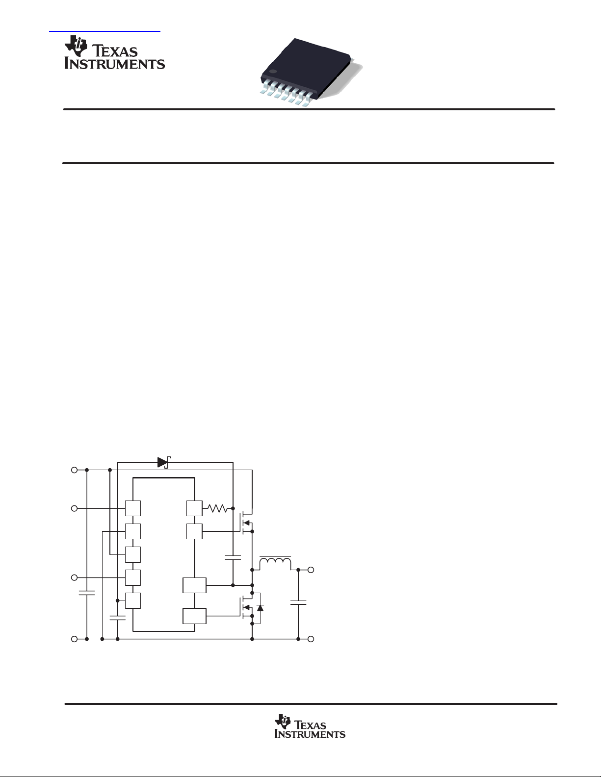
FUNCTIONAL APPLICATION DIAGRAM
V
IN
UCC27223
IN
GND
VDD
VLO
VHI
SW
G2
G1
14
13
11,12
9,10
GND
PWM
IN
GND
IN
Note: 12-V input system shown. For 5-V input only systems, see Figure 6.
7
6,8
3
2 ENBL
4,5
APPLICATIONS
Multiphase Converters in Combination With
D
the TPS40090
D Non-Isolated 3.3-V, 5-V and 12-V Input
dc-to-dc Converters for Processor Power,
General Computer, Telecom and Datacom
Applications
DESCRIPTION
The UCC27223 is a high-speed synchronous
buck drivers for today’s high-efficiency,
lower-output voltage designs. Using Predictive
Gate Drivet (PGD) control technology, these
drivers reduce diode conduction and reverse
recovery losses in the synchronous rectifier
MOSFET(s).
The UCC27223 includes an enable pin that
controls the operation of both outputs. A logic
latch is also included to keep both outputs low until
the first PWM input pulse comes in. The RDS(on)
of the SR pull-down sourcing device is also
minimized for higher frequency operations.
This closed loop feedback system detects
body-diode conduction, and adjusts deadtime
delays to minimize the conduction time interval.
This virtually eliminates body-diode conduction
while adjusting for temperature, load- dependent
delays, and for different MOSFETs. Precise gate
timing at the nanosecond level reduces the
reverse recovery time of the synchronous rectifier
V
OU
OU
MOSFET body-diode, reducing reverse recovery
losses seen in the main (high-side) MOSFET. The
lower junction temperature in the low-side
MOSFET increases product reliability. Since the
power dissipation is minimized, a higher switching
frequency can also be used, allowing for smaller
component sizes.
The UCC27223 is offered in the thermally
enhanced 14-pin PowerPADt package with
2°C/W θ
.
jc
Predictive Gate Drivet and PowerPADt are trademarks of Texas Instruments Incorporated.
!" # $%&" !# '%()$!" *!"&+
*%$"# $ " #'&$$!"# '& ",& "&# &-!# #"%&"#
#"!*!* .!!"/+ *%$" '$&##0 *&# " &$&##!)/ $)%*&
"&#"0 !)) '!!&"&#+
www.ti.com
Copyright 2003, Texas Instruments Incorporated
1
Page 2
PWM INPUT
SLUS558 − DECEMBER 2003
PWP PACKAGE
(TOP VIEW)
N/C
ENBL
VDD
VLO
PVLO
AGND
IN
T
A
−40_C to 105_C NON-INVERTING UCC27223PWP
{The PWP package is available taped and reeled. Add R suffix to device type
(e.g. UCC27223PWPR) to order quantities of 2,000 devices per reel and 90
units per tube.
1
2
3
4
5
6
7
N/C − No internal connection
AVAILABLE OPTIONS
(IN)
absolute maximum ratings over operating free-air temperature (unless otherwise noted)
14
13
12
11
10
9
8
VHI
G1
SW
SWS
G2S
G2
PGND
PACKAGED DEVICES
PowerPADt
HTSSOP−14 (PWP)
†}
Supply voltage range, VDD −0.3 to 20 V. . . . . . . . . . . . . . . . . . . . . . . . . . . . . . . . . . . . . . . . . . . . . . . . . . . . . . . . . . .
Input voltage, VHI 30 V. . . . . . . . . . . . . . . . . . . . . . . . . . . . . . . . . . . . . . . . . . . . . . . . . . . . . . . . . . . . . . . . . . . . . . . . . .
SW, SWS 20 V. . . . . . . . . . . . . . . . . . . . . . . . . . . . . . . . . . . . . . . . . . . . . . . . . . . . . . . . . . . . . . . . . . . . .
Supply current, I
including gate drive current .100 mA. . . . . . . . . . . . . . . . . . . . . . . . . . . . . . . . . . . . . . . . . . . . .
DD,
Sink current (peak) pulsed, G1/G2 4.0 A. . . . . . . . . . . . . . . . . . . . . . . . . . . . . . . . . . . . . . . . . . . . . . . . . . . . . . . . . .
Source current (peak) pulsed, G1/G2 −4.0 A. . . . . . . . . . . . . . . . . . . . . . . . . . . . . . . . . . . . . . . . . . . . . . . . . . . . . . .
Analog inputs, IN, ENBL −3.0 V to V
Power Dissipation at T
Operating junction temperature range, T
Storage temperature range, T
= 25°C (PWP package) 3 W. . . . . . . . . . . . . . . . . . . . . . . . . . . . . . . . . . . . . . . . . . . . . . . .
A
J
stg
DD
+ 0.3 V, not to exceed 15 V. . . . . . . . . . . . . . . . . . . . . . . . . . . . . . . . . . . .
−55°C to 115°C. . . . . . . . . . . . . . . . . . . . . . . . . . . . . . . . . . . . . . . . . . . .
−65°C to 150°C. . . . . . . . . . . . . . . . . . . . . . . . . . . . . . . . . . . . . . . . . . . . . . . . . . . .
Lead temperature soldering 1.6 mm (1/16 inch) from case for 10 seconds 300°C. . . . . . . . . . . . . . . . . . . . . . .
†
Stresses beyond those listed under “absolute maximum ratings” may cause permanent damage to the device. These are stress ratings only , a nd
functional operation of the device at these or any other conditions beyond those indicated under “recommended operating conditions” is not
implied. Exposure to absolute-maximum-rated conditions for extended periods may affect device reliability.
‡
All voltages are with respect to AGND and PGND. Currents are positive into, negative out of the specified terminal.
2
www.ti.com
Page 3

Regulator output voltage
V
V
mA
Low-level input threshold voltage
Low-level input threshold voltage
SLUS558 − DECEMBER 2003
ELECTRICAL CHARACTERISTICS
V
= 12-V, 1-µF capacitor from VDD to GND, 1-µF capacitor from VHI to SW, 0.1-µF and 2.2-µF capacitor from
DD
PVLO to PGND, PVLO tied to VLO, T
VLO regulator
PARAMETER TEST CONDITIONS MIN TYP MAX UNIT
Regulator output voltage
Line Regulation VDD = 12 V to 20 V 2 10
Load Regulation I
Short-circuit current
Dropout voltage, (VDD at 5% VLO drop) VLO = 6.175 V, I
(1)
undervoltage lockout
PARAMETER TEST CONDITIONS MIN TYP MAX UNIT
Start threshold voltage Measured at VLO 3.30 3.82 4.40
Minimum operating voltage after start 3.15 3.70 4.15
Hysteresis 0.07 0.12 0.20
= −40_C to 105_C for the UCC27223, TA = TJ (unless otherwise noted)
A
VDD = 12 V, I
VDD = 20 V, I
VDD = 10 V, I
= 0 mA to 100 mA 15 40
VLO
VDD = 8.5 V 220 mA
= 0 mA 6.2 6.5 6.8
VLO
= 0 mA 6.2 6.5 6.8
VLO
= 100 mA 6.1 6.5 6.9
VLO
= 100 mA 7.1 7.8 8.5 V
VLO
V
mV
V
bias currents
PARAMETER TEST CONDITIONS MIN TYP MAX UNIT
VLO bias current at VLO (ON), 5 V applications only VLO = 4.5 V, VDD = no connect 3.6 4.7 5.8
VDD bias current
VDD = 8.5 V 5.5 7.1 8.5
fIN = 500 kHz, No load on G1/G2 8 16 25
input command (IN)
PARAMETER TEST CONDITIONS MIN TYP MAX UNIT
High-level input voltage 10 V < VDD < 20 V 3.3 3.6 3.9
Low-level input voltage 10 V < VDD < 20 V 2.2 2.5 2.8
Input bias current VDD = 15 V 1 µA
input (SWS)
PARAMETER TEST CONDITIONS MIN TYP MAX UNIT
High-level input threshold voltage
Input bias current SWS = 0.0 V −0.9 −1.2 −1.5 mA
fIN = 500 kHz, t
G2S = 0.0 V
fIN = 500 kHz, t
G2S = 0.0 V
fIN = 500 kHz, t
maximum,
ON, G2
minimum,
ON, G2
minimum −100 −300 −500 mV
ON, G1
1.4 2.0 2.6
0.7 1.0 1.3
input (G2S)
PARAMETER TEST CONDITIONS MIN TYP MAX UNIT
High-level input voltage
Low-level input voltage
Input bias current G2S = 0 V −370 −470 −570 µA
NOTE 1: Ensured by design. Not production tested.
fIN = 500 kHz, t
SWS = 0.0 V
fIN = 500 kHz, t
SWS = 0.0 V
ON, G2
ON, G2
maximum,
minimum,
1.4 2.0 2.6
0.7 1.0 1.3
mA
V
V
V
www.ti.com
3
Page 4
V
ns
SLUS558 − DECEMBER 2003
ELECTRICAL CHARACTERISTICS
V
= 12-V, 1-µF capacitor from VDD to GND, 1-µF capacitor from VHI to SW, 0.1-µF and 2.2-µF capacitor from
DD
PVLO to PGND, PVLO tied to VLO, T
enable (ENBL)
PARAMETER TEST CONDITION MIN TYP MAX UNITS
V
, high-level input voltage LO to HI transition 2.25 2.45 2.85
IN_H
V
, low-level input voltage HI to LO transition 1.55 1.70 1.90
IN_L
Hysteresis 1.1
R
, enable impedance VDD = 14 V, ENBL = GND 75 112 150 kΩ
ENBL
tD3, propagation delay time
tD4, propagation delay time
tr, Rise time VLO = PVLO = 8.5 V 2.5
tf, Fall time VLO = PVLO = 8.5 V 2.5
G1 main output
PARAMETER TEST CONDITIONS MIN TYP MAX UNIT
Sink resistance SW = 0 V, VHI = 6 V , IN = 0 V, G1 = 0.5 V 0.5 0.9 1.5
Source resistance
Source current
Sink current
Rise time C = 2.2 nF from G1 to SW, VDD = 20 V 17 25
Fall time C = 2.2 nF from G1 to SW, VDD = 20 V 17 25
(2)
(1)(2)
(1)(2)
(5)
(5)
= −40_C to 105_C for the UCC27223, TA = TJ (unless otherwise noted)
A
TBD
TBD
SW = 0 V, VHI = 6 V, IN = 6.5 V, G1 = 5.5 V 10 25 45
SW = 0 V, VHI = 6 V, IN = 6.5 V, G1 = 3.0 V −3 −3.3
SW = 0 V, VHI = 6 V, IN = 0 V, G1 = 3.0 V 3 3.3
V
ns
ms
Ω
A
ns
G2 SR output
PARAMETER TEST CONDITIONS MIN TYP MAX UNIT
(2)
(2)
(1)(2)
(1)(2)
(2)
PVLO = 6.5 V, IN = 6.5 V, G1 = 0.25 V 0.5 1.6 4.0
PVLO = 6.5 V, IN = 0 V, G2 = 6.0 V 10 20 35
PVLO = 6.5 V, IN = 0 V G2 = 3.25 V 3 3.3
PVLO = 6.5 V, IN = 6.5 V G2 = 3.25 V −3 3.3
C = 2.2 nF from G2 to PGND VDD = 20 V 17 25
Ω
A
ns
Sink resistance
Source resistance
Source current
Sink current
Rise time
Fall time C = 2.2 nF from G2 to PGND VDD = 20 V 20 35
deadtime delay
PARAMETER TEST CONDITIONS MIN TYP MAX UNIT
t
OFF, G2
t
OFF, G1
Delay Step Resolution 4.0 4.5 5.2
t
ON, G1
t
ON, G1
t
ON, G2
tON, G2 maximum 54
NOTE 1: Ensured by design. Not production tested.
2: The pullup / pulldown circuits of the drivers are bipolar and MOSFET transistors in parallel. The peak output current rating is the
, IN to G2 falling 40 80 125
, IN to G1 falling 55 80 110
minimum −17
maximum 49
minimum −15
combined current from the bipolar and MOSFET transistors. The output resistance is the R
voltage on the driver output is less than the saturation voltage of the bipolar transistor.
DS(ON) of the MOSFET transistor when the
ns
4
www.ti.com
Page 5
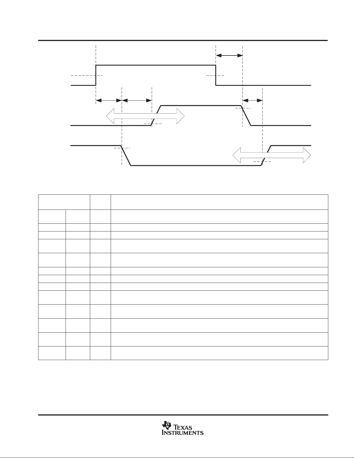
2
t
I/O
DESCRIPTION
SLUS558 − DECEMBER 2003
OFF,G1
3.25 V
G1
G2
IN
t
OFF,G2
t
On,G1
PGD
90%
10%
t
On,G2
90%
PGD
10%
UCC27223
Figure 1. Predictive Gate Drive Timing Diagram
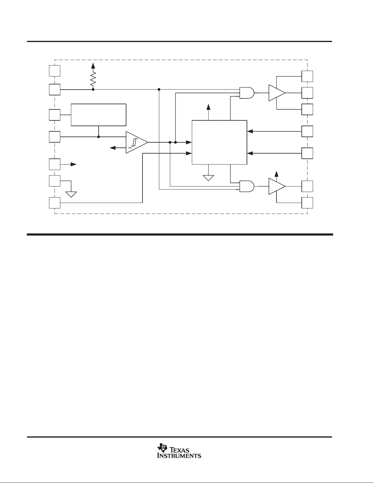
TERMINAL FUNCTIONS
TERMINAL
NAME NO.
AGND 6 −
G1 13 O High-side gate driver output that swings between SW and VHI.
G2 9 O Low-side gate driver output that swings between PGND and PVLO.
G2S 10 I
IN 7 I
PGND 8 − Ground return for the G2 driver. Connect PGND to PCB ground plane with several vias.
PVLO 5 I PVLO supplies the G2 driver. Connect PVLO to VLO and bypass on the PCB.
SW 12 − G1 driver return connection.
SWS 11 I
VDD 3 I
VHI 14 I
VLO 4 O
ENBL 2 I
Analog ground for all internal logic circuitry. AGND and PGND should be tied to the PCB ground plane
with vias.
Used by the predictive deadtime controller for sensing the SR MOSFET gate voltage to set the
appropriate deadtime.
Digital input command pin. A logic high forces on the main switch and forces off the synchronous
rectifier.
Used by the predictive controller to sense SR body-diode conduction. Connect to SR MOSFET drain
close to the MOSFET package.
Input to the internal VLO regulator. Nominal VDD range is from 8.5 V to 20 V. Bypass with at least
0.1 µF of capacitance.
Floating G1 driver supply pin. VHI is fed by an external Schottky diode during the SR MOSFET on-time.
Bypass VHI to SW with an external capacitor.
Output of the VLO regulator and supply input for the logic and control circuitry. Connect VLO to PVLO and
bypass on the PCB with a maximum capacitor value of 4.7 µF.
Enable input that controls the operation of both outputs (G1 and G2). It is internally pulled up to VLO with
a 110-kΩ resistor for active-high operation.
DESCRIPTION
UDG−0318
www.ti.com
5
Page 6
SLUS558 − DECEMBER 2003
SIMPLIFIED BLOCK DIAGRAM
NC
ENBL
VDD
VLO
PVLO
AGND
1
2
3
4
3.82 V/3.7 V
5
6
IN
7
VLO
110 kΩ
R
ENBL
VLO
REGULATOR
PVLO
+
UVLO
VLO
PREDICTIVE
DELAY
CONTROLLER
PVLO
14
VHI
13
G1
12
SW
11
SWS
10
G2S
9
G2
8 PGND
APPLICATION INFORMATION
predictive gate drive technique
The Predictive Gate Drivet technology utilizes a digital feedback system to detect body-diode conduction, and
then adjusts the deadtime delays to minimize it. This system virtually eliminates the body-diode conduction time
intervals for the synchronous MOSFET, while adjusting for different MOSFETs characteristics, propagation and
load dependent delays. Maximum power stage efficiency is the end result.
Two internal feedback loops in the predictive delay controller continuously adjusts the turn on delays for the two
MOSFET gate drives G1 and G2. As shown in Figure 2, t
body-diode conduction in the synchronous rectifier MOSFET Q
and t
OFF,G2
are fixed by propagation delays internal to the device.
The predictive delay controller is implemented using a digital control technique, and the time delays are
therefore discrete. The turn-on delays, t
ON, G1
and t
ON, G2
switching cycle. The minimum and maximum turn-on delays for G1 and G2 are specified in the electrical
characteristics table.
and t
ON,G1
. The turn-off delay for both G1 and G2, t
2
are varied to provide minimum
ON,G2
, are changed by a single step (typically 3 ns) every
OFF,G1
6
www.ti.com
Page 7

2
t
SLUS558 − DECEMBER 2003
APPLICATION INFORMATION
OFF,G1
3.25 V
G1
G2
IN
t
OFF,G2
t
On,G1
PGD
90%
10%
UCC27223
Figure 2. Predictive Gate Drive Timing Diagram
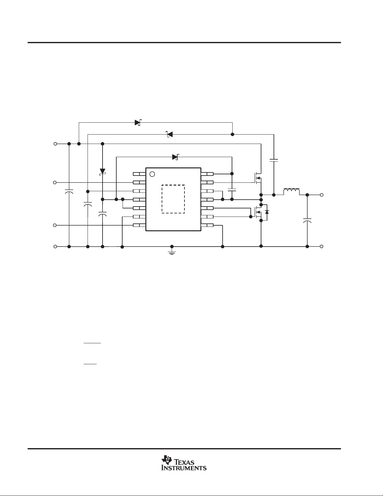
A typical application circuit for systems with 8.5-V to 20-V input is shown in Figure 3.
VIN
D1
R1
Disable
Outputs
PWM
Input
ENBL
VDD
VLO
PVLO
AGND
IN
UCC27223
VHI
G1
SW
SWS
G2S
G2
PGND
N/C
C
IN
C2
t
C1
On,G2
90%
PGD
Q1
10%
Q2
L1
Cout
UDG−0318
V
OUT
GND
Figure 3. System Application: 8.5-V to 20-V Input
www.ti.com
GND
UDG−03183
7
Page 8

SLUS558 − DECEMBER 2003
APPLICATION INFORMATION
selection of VHI series resistor R1 (dV/dt Considerations):
The series resistor R1 may be needed to slowdown the turn-on of the main forward switch to limit the dV/dt which
can inadvertently turn on the synchronous rectifier switch. In nominal 12-V input designs, a R1 value of 4-Ω to
10-Ω can be used depending on the type of MOSFET used and the high-side/low-side MOSFET ratio. In 5-V
or lower input applications however, R1 is not needed.
When the drain-source voltage of a MOSFET quickly rises, inadvertent dV/dt induced turn-on of the device is
possible. This can especially be a problem for input voltages of 12 V or greater. As Q1 rapidly turns on, the
drain-to-source voltage of Q2 rises sharply, resulting in a dV/dt voltage spike appearing on the gate signal of
Q2. If the dV/dt induced voltage spike were to exceed the given threshold voltage, the MOSFET may briefly
turn on when it should otherwise be commanded off. Obviously this undesired event would have a negative
impact on overall efficiency.
Minimizing the dV/dt effect on Q2 can be accomplished by proper MOSFET selection and careful layout
techniques. The details of how to select a MOSFET to minimize dV/dt susceptibility are outlined in SEM−1400,
Topic 2, Appendix A, Section A5. Secondly, the switch node connecting Q1, Q2 and L1 should be laid out as
tight as possible, minimizing any parasitic inductance, which might worsen the dV/dt problem.
If the dV/dt induced voltage spike is still present on the gate Q2, a 4W to 10W value of R1 is recommended to
minimize the possibility of inadvertently turning on Q2. The addition of R1 slows the turn-on of Q1, limiting the
dV/dt rate appearing on the drain-to-source of Q2. Slowing down the turn-on of Q1 will result in slightly higher
switching loss for that device only , but the efficiency gained by preventing dV/dt turn-on of Q2 will far outweigh
the negligible effect of adding R1.
When Q2 is optimally selected for dV/dt robustness and careful attention is paid to the PCB layout of the switch
node, R1 may not be needed at all, and can therefore be replaced with a 0-Ω jumper to maintain high efficiency.
The goal of the designer should not be to completely eliminate the dV/dt turn-on spike but to assure that the
maximum amplitude is less than the MOSFET gate-to-source turn-on threshold voltage under all operating
conditions.
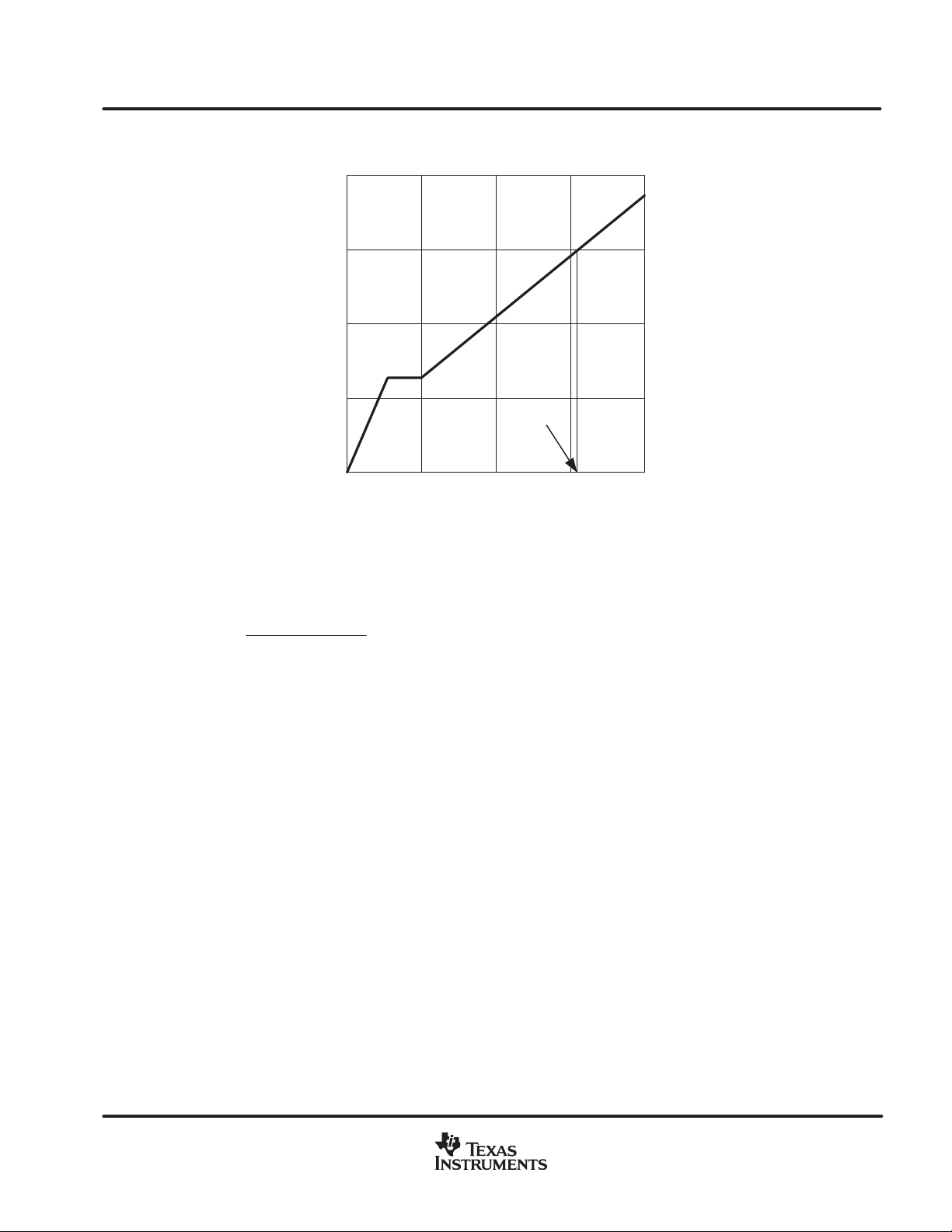
selection of bypass capacitor C1
Bypass capacitors should be selected based upon allowable ripple voltage, usually expressed as a percent of
the regulated power supply rail to be bypassed. In all of the UCC27223 application circuits shown herein, C1
provides the bypass for the main (high-side) gate driver. Every time Q1 is switched on, a packet of charge is
removed from C1 to charge Q1’s gate to approximately 6.0 V. The charge delivered to the gate of Q1 can be
found in the manufacturer’s datasheet curves. An example of a gate charge curve is shown in Figure 4.
8
www.ti.com
Page 9
(1)
SLUS558 − DECEMBER 2003
GATE-TO-SOURCE VOLTAGE
vs
31 nC
8
6
4
2
− Gate-to-Source Voltage − V
GS
V
0
020304010
TOTAL GATE CHARGE
Q6 − Total Gate Charge − nC
Figure 4.
As shown in Figure 4, 31 nC of gate charge is required in order for Q1’s gate to be charged to 6.0 V, relative
to its source. The minimum bypass capacitor value can be found using the following calculation:
Q
C1
MIN
+
k ǒVHI * V
G
Ǔ
SW
where k is the percent ripple on C1, QG is the total gate charge required to drive the gate of Q1 from zero to
the final value of (VHI−VSW). In this example gate charge curve, the value of the quantity (VHI−VSW) is taken
to be 6.0 V. This value represents the nominal VLO regulator output voltage minus the forward voltage drop of
the external Schottky diode, D1. For the MOSFET with the gate charge described in Figure 4, the minimum
capacitance required to maintain a 3% peak-to-peak ripple voltage can be calculated to be 172 nF, so a 180-nF
or a 220-nF capacitor could be used. The maximum peak-to-peak C1 ripple must be kept below 0.4 V for proper
operation.
www.ti.com
9
Page 10

(2)
SLUS558 − DECEMBER 2003
APPLICATION INFORMATION
selection of MOSFETs
The peak current rating of a driver imposes a limit on the maximum gate charge of the external power MOSFET
driven by it. The limit is based on the amount of time needed to deliver or remove the required charge to achieve
the desired switching speed during turn-on and turn-off of the external transistor. Hence, there are the families
of gate driver circuits with different current ratings.
To demonstrate this, assume a constant time interval for the switching transition and a fixed gate drive
amplitude. A larger MOSFET with more gate charge will require higher current capability from the driver to
turn-on or turn-off the device in the same amount of time. Accordingly, there is a practical upper limit on gate
charge which can be driven by the UCC27223. Considering the current capability of the TrueDrive output
stage and the available dynamic range (delay adjust range) of the Predictive Gate Drive circuitry, this limit is
approximately 120 nC of gate charge.
Some higher current applications require several MOSFETs to be connected parallel and driven by the same
gate drive signal. If their combined gate charge exceeds 120 nC, the rise and fall times of the gate drive signals
will extend and limit the delay adjust range of the PGD circuit in the UCC27223. This may limit the benefits of
the PGD technology under certain operating conditions.
Note that there are additional considerations in the gate drive circuit design which influence the maximum gate
charge of the external MOSFETs. The most significant of these is the operating frequency which, together with
the amount of gate charge, will define the power dissipation in the driver. The allowable power dissipation is a
function of the maximum junction and operating temperatures, thermal and reliability considerations.
selection of bypass capacitor C2
C2 supplies the peak current required to turn on the Q2 synchronous rectifier MOSFET, as well as the peak
current to charge the C1 capacitor through the bootstrap diode. Since the synchronous MOSFET is turned on
with 0 V across its drain-to-source, there is no Miller, or gate-to-drain charge. Therefore the synchronous
MOSFET gate can be modeled as a simple linear capacitance. The value of this capacitance can be found from
the datasheet’s gate charge curve. Referring to Figure 5, the slope of the curve past the Miller plateau indicates
the equivalent gate capacitance. Because the Y-axis is described in volts, the capacitance is actually the inverse
of the slope of the curve. For example, the curve in Figure 4 has a slope of approximately 2 V / 12 nC over the
gate charge range of 10 nC to 40 nC. The equivalent capacitance is 12 nC / 2 V = 6 nF. With the equivalent
capacitance, the minimum bypass capacitor value can be calculated as:
C
C2
where
D C
MIN
EQ
EQ
+
k
is the equivalent gate capacitance,
D k is the voltage ripple on C2, expressed as a percentage
For a peak-to-peak ripple of 3%, the minimum C2 capacitor value is calculated to be 200 nF. A 220-nF capacitor
would be used in this case. C2
low ESL by-pass capacitor should be placed as close to the UCC27223 chip as possible. The capacitor provides
the transient currents needed by the drive stage and prevents UVLO shutdown of the driver during turn-on.
should not exceed 4.7 µF. In addition to the calculated capacitance, a 100-nF
MAX
10
www.ti.com
Page 11

+3.3 V or
UT
D
(3)
(4)
SLUS558 − DECEMBER 2003
APPLICATION INFORMATION
regulator current and power dissipation
The regulator current can be calculated from the dc or average current required by the two gate drivers. This
current can be expressed as:
I
REG
+ F
SW
ǒ
CEQ VLO ) Q
Ǔ
G
Assuming all the power dissipation is internal to the device, and the internal bias current is negligible, the power
dissipated by the device is:
P
+ F
DIS
SW
ǒ
CEQ VLO ) Q
Ǔ
VDD
G
For a 500-kHz design, using MOSFETs with the gate charge characteristics shown in Figure 4 for both Q1 and
Q2, the average regulator current would be 35 mA, and, when operated from a 12-V input rail, the resulting
power dissipation is calculated to be 420 mW.
systems using 3.3-V or 5-V power input and 12-V gate drive
Figure 5 shows a schematic for systems where the power bus input is 5 V and 12 V is available for powering
the gate drives. This system provides the 6.5-V gate drive to both MOSFETs, while the power stage operates
off the 3.3-V or 5-V bus.
+5 V
Disable
Outputs
+12 V
PWM
Input
C
C3
IN
N/C
ENBL
VDD
VLO
PVLO
C2
AGND
IN
D1
UCC27223
VHI
G1
SW
SWS
G2S
G2
PGND
R1
Q1
L1
C1
Q2
Cout
V
O
GND
UDG−03184
Figure 5. System Application: 3.3-V or 5-V Power Input with 12 V Available for Gate Drive
Note that the series resistor R1 may be needed to slowdown the turn-on of the main forward switch to limit the
dV/dt which can inadvertently turn on the synchronous rectifier switch. The dV/dt considerations and the
selection of R1 are discussed in the previous section.
www.ti.com
GN
11
Page 12
(5)
(6)
SLUS558 − DECEMBER 2003
APPLICATION INFORMATION
systems with 5-V input only
The circuit pictured in Figure 6 starts up from a 5-V input bus and provides a 6.5-V gate drive to the power
MOSFETs. This circuit uses a charge pump consisting of D
and apply this to the input of the linear regulator. The regulator then regulates the doubled input voltage to the
6.5-V nominal for VLO.
D3
D4
, D4 and C3 to effectively double the input voltage
3
+5V
Disable
Outputs
PWM Input
GND
D2
C
IN
C4
C2
N/C
ENBL
VDD
VLO
PVLO
AGND
IN
D1
UCC27223
VHI
G1
SW
SWS
G2S
G2
PGND
C3
Q1
L1
C1
Q2
Cout
UDG−03185
Figure 6. System Application: 5-V-Only Power Input with 6.5-V Gate Drive Using Charge Pump Circuit
selecting D2, D3, and D
4
Selection of suitable diodes is based upon the conducted peak and average currents. D2 simply provides a path
to charge C2 at converter power-up. Virtually any one of the common BAT54 series of Schottky diodes can be
used. To select D3 and D4, the peak currents of these two diodes need to be taken into account. First, the
average current flowing in both D3 and D4 is the same as the regulator current described in equation (3). The
peak currents in D3 and D4 are described as:
V
OUT
GND
I
+
+
REG
1 * D
I
REG
D
I
D3PK
I
D4PK
For most UCC272223applications, the duty cycle is much less than 50%, and the peak current in D3 is quite
reasonable. However, the peak current in D4 is quite high. This high peak current requires using a diode with
a higher current rating for D4.
To maintain a reasonable charge pump efficiency, BAT54-type diodes can be used for applications where the
peak currents are below approximately 40 mA. For applications where the peak current is greater than 40 mA,
a 350-mA or 500-mA diode should be used. A typical 350-mA diode is SD103CW, SOD−123 package,
manufactured by Diodes Inc. A typical 500-mA diode is the ZHCS500, SOT−23 package, available from Zetex
Inc.
12
www.ti.com
Page 13

(7)
(8)
SLUS558 − DECEMBER 2003
APPLICATION INFORMATION
selection of the flying capacitor C3
The flying capacitor is subjected to large peak currents, and to keep the peak-to-peak ripple voltage low, this
capacitor has to be larger than C1 and C2. Selection of C3 should be done based on allowable peak-to-peak
ripple on C3:
I
C3
MIN
+
FSW k ǒVIN * V
REG
FD3
Ǔ
where I
V
FD2
is the regulator output current, FSW is the switching frequency, k is the percent ripple on C3, and
REG
is the forward drop of D3.
selection of bypass capacitor C4
The bypass capacitor C4 needs to be sized to take the peak current from the charge pump diode D4. The
capacitor is sized based on allowable ripple voltage:
(
C
where V
MIN
FD3
+
FSW k
and V
FD4
I
REG
ǒ
2 VIN * V
are the forward voltages of D3 and D4 and k is the percent ripple allowed on C4.
1 * D)
FD3
* V
FD4
Ǔ
enable pin and driver operation at start-up
In the UCC27223, an active-high ENBL function is implemented on pin 2. This pin when pulled low will shut off
both G1 and G2 outputs regardless of the state of the PWM input signal. The ENBL pin is pull up to VLO internally
with a 110-kΩ resistor so that the chip will be functional if the pin is left open. Enable thresholds are 2.45 V on,
and 1.7 V off. The UCC27223 also includes a logic latch to keep both outputs low at start-up even when V
is past UVLO turn-on threshold. Both outputs will always be low until the first PWM input signal comes in.
DD
www.ti.com
13
Page 14

SLUS558 − DECEMBER 2003
APPLICATION INFORMATION
synchronous rectification and predictive delay
In a normal buck converter, when the main switch turns off, current is flowing to the load in the inductor. This
current cannot be stopped immediately without using infinite voltage. For the current path to flow and maintain
voltage levels at a safe level, a rectifier or catch device is used. This device can be either a conventional diode,
or it can be a controlled active device if a control signal is available to drive it. The UCC27223 provides a signal
to drive an N-channel MOSFET as a rectifier. This control signal is carefully coordinated with the drive signal
for the main switch so that there is minimum delay from the time that the rectifier MOSFET turns off and the main
switch turns on, and minimum delay from when the main switch turns off and the rectifier MOSFET turns on.
This scheme, Predictive Gate Drivet delay, uses information from the current switching cycle to adjust the
delays that are to be used in the next cycle. Figure 7 shows the switch-node voltage waveform for a
synchronously rectified buck converter. Illustrated are the relative effects of a fixed-delay drive scheme
(constant, pre-set delays for the turnoff to turn on intervals), an adaptive delay drive scheme (variable delays
based upon voltages sensed on the current switching cycle) and the predictive delay drive scheme.
Note that the longer the time spent in body-diode conduction during the rectifier conduction period, the lower
the efficiency. Also, not described in Figure 7 is the fact that the predictive delay circuit can prevent the body
diode from becoming forward biased at all while at the same time avoiding cross conduction or shoot through.
This results in a significant power savings when the main MOSFET turns on, and minimizes reverse recovery
loss in the body diode of the rectifier MOSFET.
The power dissipation on the main (forward) MOSFET is reduced as well, although that savings is not as
significant as the savings in the rectifier MOSFET.
During reverse recovery the body diode is still forward biased, thus the reverse recovery current goes through
the forward MOSFET while the drain−source voltage is still high, causing additional switching losses. Without
PGD during this switching transition, Vds = Vin and Ids = Iload + Irr in the main MOSFET. With PGD however,
Vds = V in and Ids = Iload. The reduction in current accounts for additional power savings in the main MOSFET.
V
IN
0 V
V
D
GND
Channel Conduction
Body Diode Conduction
Fixed Delay
Adaptive Delay
Predictive Delay
UDG−02175
14
Figure 7. Switch Node Waveforms for Synchronous Buck Converter
www.ti.com
Page 15

SLUS558 − DECEMBER 2003
APPLICATION INFORMATION
comparison between predictive and adaptive gate drive techniques
The first synchronous rectifier controllers had a fixed turn-on delay between the two gate drivers. The advantage
of this well-known technique is its simplicity. The drawbacks include the need to make the delay times long
enough to cover the entire application of the device and the temperature and lot-to-lot variation of the time delay.
Since the body-diode of the synchronous rectifier conducts during this deadtime, the efficiency of this technique
varies with different MOSFETs, ambient temperature, and with the lot-to-lot variation of the deadtime delay.
To combat the variability of the internal time delays, second generation controllers used state information from
the power stage to control the turn-on of the two gate drivers. This technique is usually referred to as adaptive
gate drive technique and is pictured in FIgure 8.
V
IN
+
ON
ON
OFF
+
V
OUT
UDG−01031
Figure 8. Adaptive Gate Drive Technique
The main advantage of the adaptive technique is the on-the-fly delay adjustment for different MOSFETs and
temperature-variable time delays. The disadvantages include the body-diode conduction time intervals caused
by delays in the cross-coupling loops and the inability to compensate for the delay to charge the MOSFET gates
to the threshold levels. Additionally, i t i s d i fficult to determine whether the synchronous MOSFET channel is off
by solely monitoring the SR MOSFET gate voltage. Some devices actually add a programmable delay between
the turn-off of the synchronous rectifier and the turn-on of the main MOSFET via an external capacitor. This
added delay directly affects the power stage efficiency through additional body-diode conduction losses. Since
these losses are centralized in the synchronous MOSFET, the stress and temperature rise in this component
becomes a major design headache.
The third-generation predictive control technique is different from the adaptive technique in that it uses
information from the previous switching cycle to set the deadtime for the current cycle. The adaptive technique
on the other hand uses the current state information to set the delay times. The inherent feedback loop
propagation delays cause body-diode conduction.
www.ti.com
15
Page 16

SLUS558 − DECEMBER 2003
APPLICATION INFORMATION
adaptive vs. predictive waveforms
Figures 9 through 11 illustrate the adaptive (left) vs. predictive (right) switching waveforms. Key comparison
regions are denoted with (A), (B), (C), (D), and (E) for the adaptive control waveforms and (A′), (B′), (C′), (D′),
and (E′) for the predictive control waveforms. Figures 10 and 11 are close-ups of each transition edge.
At (A), the propagation delay from sensing the synchronous rectifier gate going low to the high-side gate going
high results in approximately 60 ns of body-diode conduction shown at (B). With the predictive drive, as soon
as the body-diode conduction of the SR MOSFET (B) is sensed, the high-side turn-on delay is adjusted to
minimize the body-diode conduction time (B′).
At (A′), the high side gate-to-source voltage is increasing while the synchronous rectifier gate-to-source voltage
is decreasing. A natural result of the precise timing of the high-side MOSFET turn-on is shown at (C) and (C′).
The overshoot and ringing for the predictive drive (C′) has much smaller amplitude than the adaptive drive (C)
due a reduction in reverse recovery in the SR MOSFET body diode. This reduction in reverse recovery is only
possible with the extremely precise gate timing used in the predictive drive technique.
At (D), the propagation delay from the synchronous rectifier drain-to-source voltage falling to the gate-to-source
voltage rising causes the body diode of the SR MOSFET to conduct for approximately 60 ns (E). When the
predictive drive is enabled (D′), the inherent delay is eliminated and virtually no body-diode conduction is shown
at (E′).
A
C
B
Adaptive Drive
Complementary
D
E
100 ns / div
Gate Drive
Waveforms
2 V / div
VDS of SR
MOSFET
Switch
2 V / div
Figure 9. Adaptive vs. Predictive Switching Waveforms
A4
C4
B4
Predictive Drive
100 ns / div
D4
E4
16
www.ti.com
Page 17

SLUS558 − DECEMBER 2003
APPLICATION INFORMATION
A4
B4
20 ns / div
Adaptive Drive
20 ns / div
Complementary
A
C
B
Gate Drive
Waveforms
2 V / div
VDS of SR
MOSFET
Switch
2 V / div
Predictive Drive
Figure 10. Close-Up: Turn-Off of Synchronous Rectifier Switch to Turn-On of Main Switch
Complementary
Gate Drive
D
E
Waveforms
2 V / div
VDS of SR
MOSFET
Switch
2 V / div
D4
E4
C4
Adaptive Drive
20 ns / div
Predictive Drive
20 ns / div
Figure 11. Close-Up: Turn-Off of Main Switch to Turn-On of Synchronous Rectifier Switch
efficiency comparison
Figures 12 through 15 show a series of efficiency measurements taken at two output voltages (0.9 V and 1.8
V) and two switching frequencies (250 kHz and 500 kHz) for both predictive and adaptive delay techniques.
The efficiency gain using the predictive technique is 1% for a V
of 250 kHz (Figure 12). Figures 13 and 14 show the efficiency gain approximately doubles when V
by a factor of two (to 0.9 V), or when the switching frequency is doubled to 500 kHz. With both doubled frequency
and one-half of the output voltage, the efficiency gain of predictive technology is about 4% over the adaptive
technology (Figure 15). Therefore, as the switching frequency increases and output voltages are lowered, the
efficiency gains are higher. This results in lower operational temperatures for increased reliability as well as
smaller size designs for increased frequencies.
level of 1.8 V and at a switching frequency
OUT
OUT
is lowered
www.ti.com
17
Page 18

SLUS558 − DECEMBER 2003
APPLICATION INFORMATION
EFFICIENCY
vs
OUTPUT CURRENT
96
94
92
90
88
86
84
Efficiency − %
82
80
78
76
74
0 5 10 15 20
ADAPTIVE
I
OUT
− Output Current − A
PREDICTIVE
DELTA POWER
DISSIPATION
VIN = 5 V
V
= 1.8 V
OUT
fSW = 250 kHz
Figure 12
EFFICIENCY
vs
OUTPUT CURRENT
96
94
92
90
88
86
84
Efficiency − %
82
80
78
76
74
0 5 10 15 20
ADAPTIVE
DELTA POWER
DISSIPATION
I
OUT
− Output Current − A
PREDICTIVE
VIN = 5 V
V
= 1.8 V
OUT
fSW = 500 kHz
Figure 14
0.5
0.4
0.3
0.2
0.1
0.0
1.2
1.0
0.8
0.6
0.4
0.2
0.0
96
VIN = 5 V
V
94
fSW = 250 kHz
92
90
88
86
84
82
Efficiency − %
80
Delta Power Dissipation − W
78
76
74
0 5 10 15 20
96
VIN = 5 V
94
V
OUT
fSW = 500 kHz
92
90
88
86
84
Efficiency − %
82
80
Delta Power Dissipation − W
78
76
74
0 5 10 15 20
= 0.9 V
OUT
ADAPTIVE
= 0.9 V
ADAPTIVE
EFFICIENCY
vs
OUTPUT CURRENT
PREDICTIVE
DELTA POWER
DISSIPATION
I
− Output Current − A
OUT
Figure 13
EFFICIENCY
vs
OUTPUT CURRENT
PREDICTIVE
DELTA POWER
DISSIPATION
I
− Output Current − A
OUT
Figure 15
0.5
0.4
0.3
0.2
0.1
Delta Power Dissipation − W
0.0
1.2
1.0
0.8
0.6
0.4
Delta Power Dissipation − W
0.2
0.0
18
www.ti.com
Page 19

SLUS558 − DECEMBER 2003
LAYOUT CONSIDERATIONS
packaging
The UCC27223 is only available in TI’s thermally enhanced 14-pin PowerPad package. This package offers
exceptional thermal impedance with a junction-to-case rating of 2_C/W. Shown as the crosshatched region in
Figure 16, PowerPad includes an exposed leadframe die pad located on the bottom side of the package.
Exposed pad dimensions for the PowerPadt TSSOP 14-pin package are 69 mils x 56 mils (1.8 mm x 1.4 mm).
However, the exposed pad tolerances can be + 41 / − 2 mils (+ 1.05 /− .05 mm) due to position and mold flow
variation. Effectively removing the heat from the PowerPAD package requires a thermal land area, shown as
the shaded gray region in Figure 16, designed into the PCB directly beneath the package. A minimum thermal
land area of 5 mm by 3.4 mm is recommended as illustrated in Figure 16. Any tolerance variances of the exposed
PowerPad falls well within the thermal land area when the recommended minimum land area is included on
the printed circuit board. In addition, a 2-by-3 array of 13-mil thermal vias is required within the exposed
PowerPad area, as shown in Figure 16. If additional heat sinking capability is required, larger 25-mil vias can
be added to the thermal land area.
Required Vias on PowerPad Area
2 x 3 Array
0.33mm
(13 mil) dia Vias
0.65mm
(0.0256”)
3.4mm
(0.1339”)
0.3mm
(0.0118”)
1.05mm
(0.0413”)
Exposed
PowerPad
1.4mm (0.056”)
Exposed
PowerPad
1.8mm (0.069”)
Optional Vias on Thermal Land Area
0.635mm
(25 mil) dia Vias
5.0mm
(0.1968”)
Figure 16. TSSOP−14PWP Package Outline and Minimum PowerPADE PCB Thermal Land
www.ti.com
19
Page 20

SLUS558 − DECEMBER 2003
REFERENCE DESIGN AND EVALUATION MODULE
A reference design is discussed in, 5 V to 0.9 V − 1.8 V (adjustable), 20-A High Efficiency Synchronous Buck
Converter Using the UCC27223 with Predictive Gate Drivet, TI Literature Number SLUU181 and
accompanying evaluation module UCC27223EVM. The design highlights UCC27223 and its Predictive Gate
Drivet synchronous buck operation using a simple single ended PWM controller. The schematic is shown in
Figure 17.
+
+
20
Figure 17. Typical Application Diagram
www.ti.com
Page 21

SLUS558 − DECEMBER 2003
TYPICAL CHARACTERISTICS
BIAS CURRENT
vs
TEMPERATURE (NO LOAD)
16
14
12
10
8
− Bias Current − mA
6
SUPPLY
4
I
2
0
IDD: VDD = 12 V, 500 kHz
IDD: VDD = 8.5 V, Static
I
: VLO = 12 V, Static, 5 V Only Systems
VLO
−50 −25 0 25 50 75 100 125
TA − Temperature − °C
Figure 18
UVLO THRESHOLD
vs
TEMPERATURE
4.2
4.1
4.0
3.9
3.8
3.7
3.6
UVLO Threshold − V
3.5
3.4
3.3
3.2
−50 −25 0 25 50 75 100 125
UVLO On
UVLO Off
TA − Temperature − °C
Figure 19
VLO LINE REGULATION
vs
TEMPERATURE (NO LOAD, IVLO = 0 mA)
6.8
6.7
6.6
VDD = 20 V
6.5
− Line Regulation − V
6.4
LO
V
6.3
6.2
−50 −25 0 25 50 75 100 125
TA − Temperature − °C
VDD = 12 V
Figure 20
VLO LOAD REGULATION
vs
TEMPERATURE
6.8
6.7
6.6
I
= 0 mA
VLO
6.5
I
= 100 mA
VLO
6.4
− Load Regulation − V
LO
V
6.3
6.2
−50 −25 0 25 50 75 100 125
TA − Temperature − °C
Figure 21
www.ti.com
21
Page 22

SLUS558 − DECEMBER 2003
TYPICAL CHARACTERISTICS
DROPOUT VOLTAGE (VDD AT VLO = 6.175 V)
vs
OUTPUT CURENT
8.6
8.4
8.2
8.0
7.8
− Dropout Voltage − V
7.6
DD
V
7.4
7.2
7.0
0 50 100
IVLO − VLO Output Current − mA
Figure 22
DROPOUT VOLTAGE (VDD AT VLO = 6.175 V)
vs
TEMPERATURE (I
8.6
8.4
8.2
8.0
7.8
7.6
− Dropout Voltage − V
DD
V
7.4
7.2
7.0
−50 25 125
TA − Temperature − °C
= 100 mA)
VLO
Figure 23
10075500−25
VLO SHORT CIRCUIT CURRENT
vs
TEMPERATURE
300
290
280
270
260
250
240
230
− Short Circuit Current − mA
LO
220
V
210
200
−50 25 125
TA − Temperature − °C
Figure 24
INPUT THRESHOLD
vs
TEMPERATURE (VDD = 10 V TO 20 V)
4.0
Input Threshold Rising
3.5
3.0
Input Threshold Falling
2.5
2.0
1.5
Input Threshold − V
1.0
0.5
0.0
10075500−25
−50 25 125
Input Threshold Hyst.
10075500−25
TA − Temperature − °C
Figure 25
22
www.ti.com
Page 23

SLUS558 − DECEMBER 2003
TYPICAL CHARACTERISTICS
PREDICTIVE DELAY BIT WEIGHT
vs
TEMPERATURE
4.7
4.5
4.3
4.1
3.9
PGD Step Resolution − ns
3.7
3.5
−50 25 125
TA − Temperature − °C
Figure 26
PROPAGATION DELAYS
vs
TEMPERATURE
120
100
t
, G2
OFF
80
t
, G1
OFF
60
− Propagation Delays − ns
40
PROP
t
20
0
10075500−25
−50 25 125
TA − Temperature − °C
10075500−25
Figure 27
PREDICTIVE DELAY RANGE
vs
60
50
40
30
20
10
− G1 Delay Range − ns
ON
t
−10
−20
−30
tON, G1 Max
0
−50 25 125
TEMPERATURE
tON, G1 Min
TA − Temperature − °C
Figure 28
PREDICTIVE DELAY RANGE
vs
TEMPERATURE
60
50
40
30
20
10
− G2 Delay Range − ns
0
ON
t
−10
−20
−30
10075500−25
−50 25 125
tON, G2 Max
tON, G2 Min
10075500−25
TA − Temperature − °C
Figure 29
www.ti.com
23
Page 24

SLUS558 − DECEMBER 2003
TYPICAL CHARACTERISTICS
G1 RISE AND FALL TIMES
vs
TEMPERATURE (2.2 nF)
30
25
20
− ns
F
, t
15
R
G1 t
10
5
0
Rise Time
Fall Time
−50 25 125
TA − Temperature − °C
Figure 30
G2 RISE AND FALL TIMES
vs
TEMPERATURE (2.2 nF)
30
25
20
− ns
F
, t
15
R
G2 t
10
5
0
10075500−25
−50 25 125
Fall Time
Rise Time
10075500−25
TA − Temperature − °C
Figure 31
G1 SINK RESISTANCE
vs
TEMPERATURE (R
1.5
1.4
1.3
1.2
1.1
− Ω
1.0
SINK
G1 R
0.9
0.8
0.7
0.6
0.5
−50 25 125
TA − Temperature − °C
DS(on)
)
Figure 32
G1 SOURCE RESISTANCE
vs
TEMPERATURE
40
35
30
25
− Ω
20
SOURCE
15
G1 R
10
5
0
10075500−25
−50 25 125
TA − Temperature − °C
10075500−25
Figure 33
24
www.ti.com
Page 25

5
G2 SINK RESISTANCE
SLUS558 − DECEMBER 2003
TYPICAL CHARACTERISTICS
G2 SOURCE RESISTANCE
vs
TEMPERATURE
40
vs
TEMPERATURE (R
DS(on)
)
40
35
30
25
− Ω
20
SINK
G2 R
15
10
5
0
−50 25 12
TA − Temperature − °C
Figure 34
7
10075500−25
VHI CURRENT
vs
FREQUENCY
35
30
25
− Ω
20
SOURCE
15
G2 R
10
5
0
−50 25 125
TA − Ambient Temperature − °C
Figure 35
10075500−25
6
5
4
3
VHI Current − mA
2
1
0
0 200 400 600 800 1000 1200
Frequency − kHz
Figure 36
www.ti.com
25
Page 26

SLUS558 − DECEMBER 2003
RELATED PRODUCTS
PART
NUMBER
TPS40090 High Frequency 2, 3, 4−Phase Multiphase Controller − TSSOP−24
UCC27221/2 High Efficiency Predictive Synchronous Buck ± 3.3 A PowerPADt HTSSOP−14
TPS2830/1 Fast synchronous buck MOSFET drivers with dead-time control ± 2.4 A PowerPADt HTSSOP−14, SOIC−14
TPS2832/3 Fast synchronous buck MOSFET drivers with dead-time control ± 2.4 A SOIC−8
TPS2834/5 Synchronous buck MOSFET drivers with dead-time control ± 2.4 A PowerPADt HTSSOP−14, SOIC−14
TPS2836/7 Synchronous buck MOSFET drivers with dead-time control ± 2.4 A SOIC−8
TPS2838/9 Synchronous buck MOSFET drivers with drive regulator ± 4 A PowerPADt HTSSOP−16
TPS2848/9 Synchronous buck MOSFET drivers with drive regulator ± 4 A PowerPADt HTSSOP−14
DESCRIPTION
GATE
DRIVE
PACKAGE
REFERENCES
1. Power Supply Design Seminar SEM−1400 Topic 2: Design and Application Guide for High Speed MOSFET
Gate Drive Circuits, by Laszlo Balogh, Texas Instruments Literature Number SLUP169.
2. User’s Guide: 5 V to 0.9 V − 1.8 V (adjustable), 20-A High−Efficiency Synchronous Buck Converter using
UCC27223 with Predictive Gate Drivet, TI Literature Number SLUU181.
3. User’s Guide: 12 V to 1.8 V, 20 A High-Efficiency Synchronous Buck Converter Using UCC27222 With
Predictive Gate Drivet Technology, TI Literature Number SLUU140.
4. Application Note: UCC27221/2 Predictive Gate Drivet FAQ, TI Literature Number SLUA280.
5. Application Note: Predictive Gate Drivet Boosts Converter Efficiency, TI Literature Number SLUA281.
6. Application Note: Increasing UCC27221/2 Gate Drive Voltage, TI Literature Number SLUA292.
26
www.ti.com
Page 27

20 PINS SHOWN
SLUS558 − DECEMBER 2003
MECHANICAL DATA
PWP (R-PDSO-G**) PowerPAD PLASTIC SMALL-OUTLINE
0,65
20
1
1,20 MAX
0,30
0,19
11
4,50
4,30
10
A
0,15
0,05
PINS **
DIM
M
0,10
6,60
6,20
Seating Plane
0,10
1614
Thermal Pad
(See Note F)
20
0,15 NOM
0°−ā 8°
Gage Plane
0,25
0,75
0,50
2824
A MAX
A MIN
NOTES: A. All linear dimensions are in millimeters.
B. This drawing is subject to change without notice.
C. Body dimensions do not include mold flash or protrusions.
D. The package thermal performance may be enhanced by attaching an external heat sink to the thermal pad.
This pad is electrically and thermally connected to the backside of the die.
E. Falls within JEDEC MO-153
F. The PowerPAD
substrate which is the ground of the device. The exposed pad dimension is 1.4 mm x 1.8 mm. However, the tolerances can be
+1.05/−0.05 mm (+ 41 / −2 mils) due to position and mold flow variation.
G. For additional information on the PowerPADt package and how to take advantage of its heat dissipating abilities, refer to Technical
Brief, PowerPad Thermally Enhanced Package, Texas Instrument s Literature No. SLMA002 and Application Brief, PowerPad Made
Easy, Texas Instruments Literature No. SLMA004. Both documents are available at www.ti.com.
is not directly connected to any leads of the package. However, it is electrically and thermally connected to the
5,10
4,90
5,10
4,90
6,60
6,40
7,90
7,70
9,80
9,60
4073225/F 10/98
www.ti.com
27
Page 28

PACKAGE OPTION ADDENDUM
www.ti.com
16-May-2005
PACKAGING INFORMATION
Orderable Device Status
(1)
Package
Type
Package
Drawing
Pins Package
Qty
Eco Plan
UCC27223PWP ACTIVE HTSSOP PWP 14 90 Green (RoHS &
no Sb/Br)
UCC27223PWPG4 ACTIVE HTSSOP PWP 14 90 Green (RoHS &
no Sb/Br)
UCC27223PWPR ACTIVE HTSSOP PWP 14 2000 Green (RoHS &
no Sb/Br)
UCC27223PWPRG4 ACTIVE HTSSOP PWP 14 2000 Green (RoHS &
no Sb/Br)
(1)
The marketing status values are defined as follows:
ACTIVE: Product device recommended for new designs.
LIFEBUY: TI has announced that the device will be discontinued, and a lifetime-buy period is in effect.
NRND: Not recommended for new designs. Device is in production to support existing customers, but TI does not recommend using this part in
a new design.
PREVIEW: Device has been announced but is not in production. Samples may or may not be available.
OBSOLETE: TI has discontinued the production of the device.
(2)
Eco Plan - The planned eco-friendly classification: Pb-Free (RoHS) or Green (RoHS & no Sb/Br) - please check
http://www.ti.com/productcontent for the latest availability information and additional product content details.
TBD: The Pb-Free/Green conversion plan has not been defined.
Pb-Free (RoHS): TI's terms "Lead-Free" or "Pb-Free" mean semiconductor products that are compatible with the current RoHS requirements
for all 6 substances, including the requirement that lead not exceed 0.1% by weight in homogeneous materials. Where designed to be soldered
at high temperatures, TI Pb-Free products are suitable for use in specified lead-free processes.
Green (RoHS & no Sb/Br): TI defines "Green" to mean Pb-Free (RoHS compatible), and free of Bromine (Br) and Antimony (Sb) based flame
retardants (Br or Sb do not exceed 0.1% by weight in homogeneous material)
(2)
Lead/Ball Finish MSL Peak Temp
CU NIPDAU Level-2-260C-1 YEAR
CU NIPDAU Level-2-260C-1 YEAR
CU NIPDAU Level-2-260C-1 YEAR
CU NIPDAU Level-2-260C-1 YEAR
(3)
(3)
MSL, Peak Temp. -- The Moisture Sensitivity Level rating according to the JEDEC industry standard classifications, and peak solder
temperature.
Important Information and Disclaimer:The information provided on this page represents TI's knowledge and belief as of the date that it is
provided. TI bases its knowledge and belief on information provided by third parties, and makes no representation or warranty as to the
accuracy of such information. Efforts are underway to better integrate information from third parties. TI has taken and continues to take
reasonable steps to provide representative and accurate information but may not have conducted destructive testing or chemical analysis on
incoming materials and chemicals. TI and TI suppliers consider certain information to be proprietary, and thus CAS numbers and other limited
information may not be available for release.
In no event shall TI's liability arising out of such information exceed the total purchase price of the TI part(s) at issue in this document sold by TI
to Customer on an annual basis.
Addendum-Page 1
Page 29

Page 30

IMPORTANT NOTICE
Texas Instruments Incorporated and its subsidiaries (TI) reserve the right to make corrections, modifications,
enhancements, improvements, and other changes to its products and services at any time and to discontinue
any product or service without notice. Customers should obtain the latest relevant information before placing
orders and should verify that such information is current and complete. All products are sold subject to TI’s terms
and conditions of sale supplied at the time of order acknowledgment.
TI warrants performance of its hardware products to the specifications applicable at the time of sale in
accordance with TI’s standard warranty. Testing and other quality control techniques are used to the extent TI
deems necessary to support this warranty . Except where mandated by government requirements, testing of all
parameters of each product is not necessarily performed.
TI assumes no liability for applications assistance or customer product design. Customers are responsible for
their products and applications using TI components. To minimize the risks associated with customer products
and applications, customers should provide adequate design and operating safeguards.
TI does not warrant or represent that any license, either express or implied, is granted under any TI patent right,
copyright, mask work right, or other TI intellectual property right relating to any combination, machine, or process
in which TI products or services are used. Information published by TI regarding third-party products or services
does not constitute a license from TI to use such products or services or a warranty or endorsement thereof.
Use of such information may require a license from a third party under the patents or other intellectual property
of the third party, or a license from TI under the patents or other intellectual property of TI.
Reproduction of information in TI data books or data sheets is permissible only if reproduction is without
alteration and is accompanied by all associated warranties, conditions, limitations, and notices. Reproduction
of this information with alteration is an unfair and deceptive business practice. TI is not responsible or liable for
such altered documentation.
Resale of TI products or services with statements different from or beyond the parameters stated by TI for that
product or service voids all express and any implied warranties for the associated TI product or service and
is an unfair and deceptive business practice. TI is not responsible or liable for any such statements.
Following are URLs where you can obtain information on other Texas Instruments products and application
solutions:
Products Applications
Amplifiers amplifier.ti.com Audio www.ti.com/audio
Data Converters dataconverter.ti.com Automotive www.ti.com/automotive
DSP dsp.ti.com Broadband www.ti.com/broadband
Interface interface.ti.com Digital Control www.ti.com/digitalcontrol
Logic logic.ti.com Military www.ti.com/military
Power Mgmt power.ti.com Optical Networking www.ti.com/opticalnetwork
Microcontrollers microcontroller.ti.com Security www.ti.com/security
Telephony www.ti.com/telephony
Video & Imaging www.ti.com/video
Wireless www.ti.com/wireless
Mailing Address: Texas Instruments
Post Office Box 655303 Dallas, Texas 75265
Copyright 2005, Texas Instruments Incorporated
 Loading...