

Datasheet UC5603QPTR, UC5603QP, UC5603N, UC5603J, UC5603DPTR Datasheet (Texas Instruments)
...
• Complies with SCSI, SCSI-2 and
SPI-2 Standards
• 6pF Channel Capacitance during
Disconnect
• 100µA Supply Current in
Disconnect Mode
• Meets SCSI Hot Plugging
• -400mA Sourcing Current for
Termination
• +400mA Sinking Current for
Active Negation Drivers
• Logic Command Disconnects all
Termination Lines
• Trimmed Termination Current to
3%
• Trimmed Impedance to 3%
• Negative Clamping on all Signal
Lines
• Current Limit and Thermal
Shutdown Protection
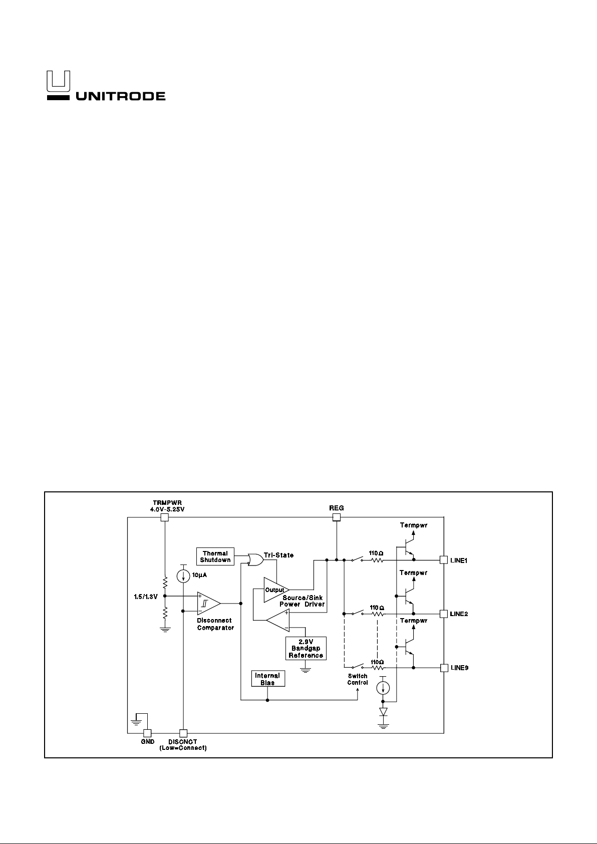
The UC5603 provides 9 lines of active termination for a SCSI (Small Computers Systems Interface) parallel bus. The SCSI standard recommends active
termination at both ends of the cable segment.
The UC5603 provides a disconnect feature which, when opened or driven
high, will disconnect all terminating resistors, and disables the regulator;
greatly red uc ing standby power. The output channels remain high impedance
even without Termpwr applied. A low channel capacitance of 6pF allows units
at interim points of the bus to have little to no effect on the signal integrity.
Functionall y the UC5603 is s imilar to its pr edecessor, the UC5601 - 18 line
Active Terminator. Several electrical enhancements were incorporated in the
UC5603, suc h as a sink/source re gulator output stage t o accommodate all
signal lin es at + 5V, while the regulator remains at its nominal value, reduced
channel cap acitance to 6pF typical, and as with the UC5601, custom power
packages are utilized to allow normal operation at full power conditions (1.2
watts).
Internal ci rcuit trimming is uti lized, first to trim the impedance to a 3% tolerance, and then mo st imp ort antl y, to trim the output current to a 3% tolerance,
as close to the max SCSI spec as possible, which maximizes noise margin in
fast SCSI operation.
Other feat ures include negative cl amping on all signal lines to protect external circuitry from latch-up, thermal shutdown and current limit.
This device is offered in low thermal resistance versions of the industry standard 16 pin narrow body S OIC, 16 pin ZIP (zig-zag in line pac kage) and 24 pin
TSSOP.
UC5603
9-Line SCSI Active Terminator
FEATURES DESCRIPTION
BLOCK DIAGRAM
Circuit Design Patented
3/97
UDG-94049
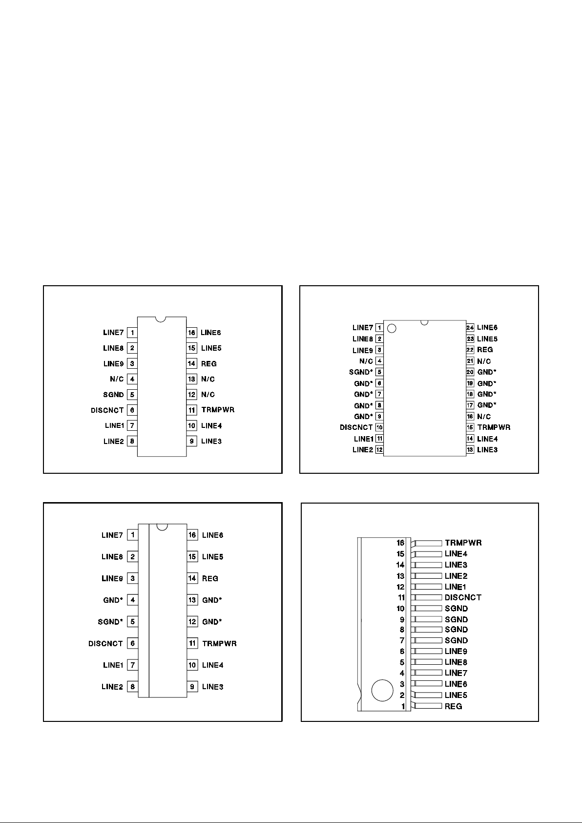
DIL-16 (Top View)
N or J Package
* DP packag e pi n 5 se rves as signal ground; pins 4, 12, 13
serve as heatsink/ground.
ZIP-16 (Top View)
Z Package
SOIC-16 (Top View)
DP Package
TSSOP-24 (To p View)
PWP Package
Note: Drawings are not to scale.
UC5603
Termpwr Vo ltage . . . . . . . . . . . . . . . . . . . . . . . . . . . . . . . . . . . . . . . . . . . . . . . . . . . +7V
Signal Line Voltage. . . . . . . . . . . . . . . . . . . . . . . . . . . . . . . . . . . . . . . . . . . . . 0V to +7V
Regulator Output Current . . . . . . . . . . . . . . . . . . . . . . . . . . . . . . . . . . . . . . . . . . . . 0.5A
Storage Temperature . . . . . . . . . . . . . . . . . . . . . . . . . . . . . . . . . . . . . −65°C to +150°C
Operating Temperature . . . . . . . . . . . . . . . . . . . . . . . . . . . . . . . . . . . −55°C to +150°C
Lead Temperature (Soldering, 10 Sec.) . . . . . . . . . . . . . . . . . . . . . . . . . . . . . . . +300°C
ABSOLUTE MAXIMUM RATINGS
Termpwr Voltage . . . . . . . . . . . . . . . . . . . . . . . . . . . . . . . . . . . . . . . . . . . 3.8V to 5.25V
Signal Line Voltage. . . . . . . . . . . . . . . . . . . . . . . . . . . . . . . . . . . . . . . . . . . . . 0V to +5V
Disconnect Input Voltage . . . . . . . . . . . . . . . . . . . . . . . . . . . . . . . . . . . . 0V to Termpwr
RECOMMENDED OPERATING CONDITIONS
CONNECTION DIAGRAMS
Unless otherwise sp ec ified all voltages are with respe ct to Ground. Currents are positive into, negative out of the specified terminal.
Consult Packaging Section of Unitrode Integrated Circuits databook for thermal limitations and consid era ti on s of pac ka ges.
* PWP package pin 5 serves as signal ground; pin s 6, 7, 8, 9,
17, 18, 19, and 20 serve as heatsink/ground.
2
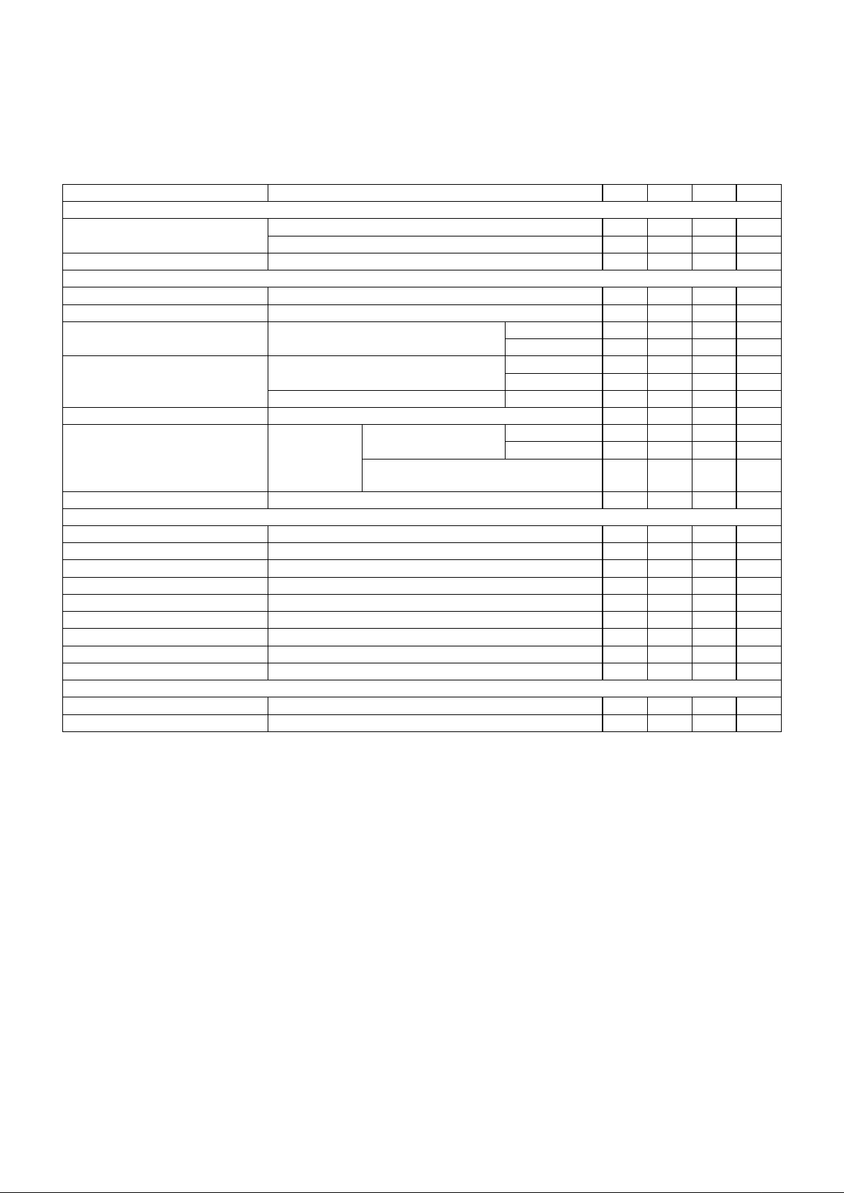
PARAMETER TEST CONDITIONS MIN TYP MAX UNITS
Supply Current Section
Termpwr Supply Current All termination lines = Open 12 18 mA
All termination li ne s = 0. 5V 200 220 mA
Power Down Mode DISCNCT = Open 100 150 µA
Output Section (Termina tor Li ne s)
Terminator Impedance ∆I
LINE
= -5mA to -15mA 107 110 113 Ohms
Output High Voltage V
TRMPWR
= 4V (Note 1) 2.7 2.9 V
Max Output Cur r e nt V
LINE
= 0.5V TJ = 25°C -21.1 -21.9 -22.4 mA
0°C < T
J
< 70°C -20.5 -21.9 -22.4 mA
Max Output Cur r e nt V
LINE
= 0.5V, TRMPWR = 4V (Note 1) TJ = 25°C -20.3 -21.9 -22.4 mA
0°C < T
J
< 70°C -19.8 -21.9 -22.4 mA
V
LINE
= 0.2V, TRMPWR = 4.0V to 5.25V 0°C < TJ < 70°C –22.0 –24.0 –25.4 mA
Output Clamp Level I
LINE
= -30mA -0.2 -0.05 0.1 V
Output Leakage
DISCNCT = 4V
TRMPWR = 0V to 5.25V
REG = 0V
V
LINE
= 0 to 4V 10 400 n A
V
LINE
= 5.25V 100 µA
TRMPWR = 0V to 5.25V, REG = Open
V
LINE
= 0V to 5.25V
10 400 nA
Output Capacitance DISCNCT = Open (Note 2) (DP Package) 6 8 pF
Regulator Section
Regulator Output Voltage 2.8 2.9 3 V
Regulator Output Voltage All Termination Lines = 5V 2.8 2.9 3 V
Line Regulation TRMPWR = 4V to 6V 10 20 mV
Load Regulation I
REG
= +100mA to -100mA 20 50 mV
Drop Out Voltage All Termination Lines = 0.5V 0.7 1 V
Short Circuit Current V
REG
= 0V -200 -400 -600 mA
Sinking Current Capability V
REG
= 3.5V 200 400 600 mA
Thermal Shutdown 170 °C
Thermal Shutdown Hysteresis 10 °C
Disconnect Section
Disconnect Threshold 1.3 1.5 1.7 V
Threshold Hysteresis 100 160 250 mV
ELECTRICAL CHARACTERISTICS
Unless otherwise st at ed, th ese sp ecif icat io ns app ly for TA= 0°C to 70°C.
TRMPWR = 4.75V DISCNCT = 0V. TA = TJ.
UC5603
Note 1: Measuring each termination line while other 8 are low (0.5V).
Note 2: Guaranteed by des ig n. Not 100% tested in production.
3

Figure 1:
T ypical Wide SCSI Bus Configurations Utilizing 1 UC5601 and 1 UC5603 Device
Figure 2:
Typical Wide SCSI Bus Configurations Utilizing 3 UC5603 Devices.
UC5603
APPLICATION INFORMATION
UDG-94051
UDG-94050
UNITRODE CORPORATI ON
7 CONTINENTAL BLVD. • MERRIMACK, NH 03054
TEL. (603) 424- 24 10 • FAX (603) 424-3460
4

IMPORTANT NOTICE
T exas Instruments and its subsidiaries (TI) reserve the right to make changes to their products or to discontinue
any product or service without notice, and advise customers to obtain the latest version of relevant information
to verify, before placing orders, that information being relied on is current and complete. All products are sold
subject to the terms and conditions of sale supplied at the time of order acknowledgement, including those
pertaining to warranty, patent infringement, and limitation of liability.
TI warrants performance of its semiconductor products to the specifications applicable at the time of sale in
accordance with TI’s standard warranty. Testing and other quality control techniques are utilized to the extent
TI deems necessary to support this warranty. Specific testing of all parameters of each device is not necessarily
performed, except those mandated by government requirements.
CERT AIN APPLICATIONS USING SEMICONDUCTOR PRODUCTS MAY INVOLVE POTENTIAL RISKS OF
DEATH, PERSONAL INJURY, OR SEVERE PROPERTY OR ENVIRONMENTAL DAMAGE (“CRITICAL
APPLICATIONS”). TI SEMICONDUCTOR PRODUCTS ARE NOT DESIGNED, AUTHORIZED, OR
WARRANTED TO BE SUITABLE FOR USE IN LIFE-SUPPORT DEVICES OR SYSTEMS OR OTHER
CRITICAL APPLICATIONS. INCLUSION OF TI PRODUCTS IN SUCH APPLICA TIONS IS UNDERSTOOD T O
BE FULLY AT THE CUSTOMER’S RISK.
In order to minimize risks associated with the customer’s applications, adequate design and operating
safeguards must be provided by the customer to minimize inherent or procedural hazards.
TI assumes no liability for applications assistance or customer product design. TI does not warrant or represent
that any license, either express or implied, is granted under any patent right, copyright, mask work right, or other
intellectual property right of TI covering or relating to any combination, machine, or process in which such
semiconductor products or services might be or are used. TI’s publication of information regarding any third
party’s products or services does not constitute TI’s approval, warranty or endorsement thereof.
Copyright 1999, Texas Instruments Incorporated
 Loading...