

UC5350
PRELIMINARY
SLUS258A - MARCH 2000
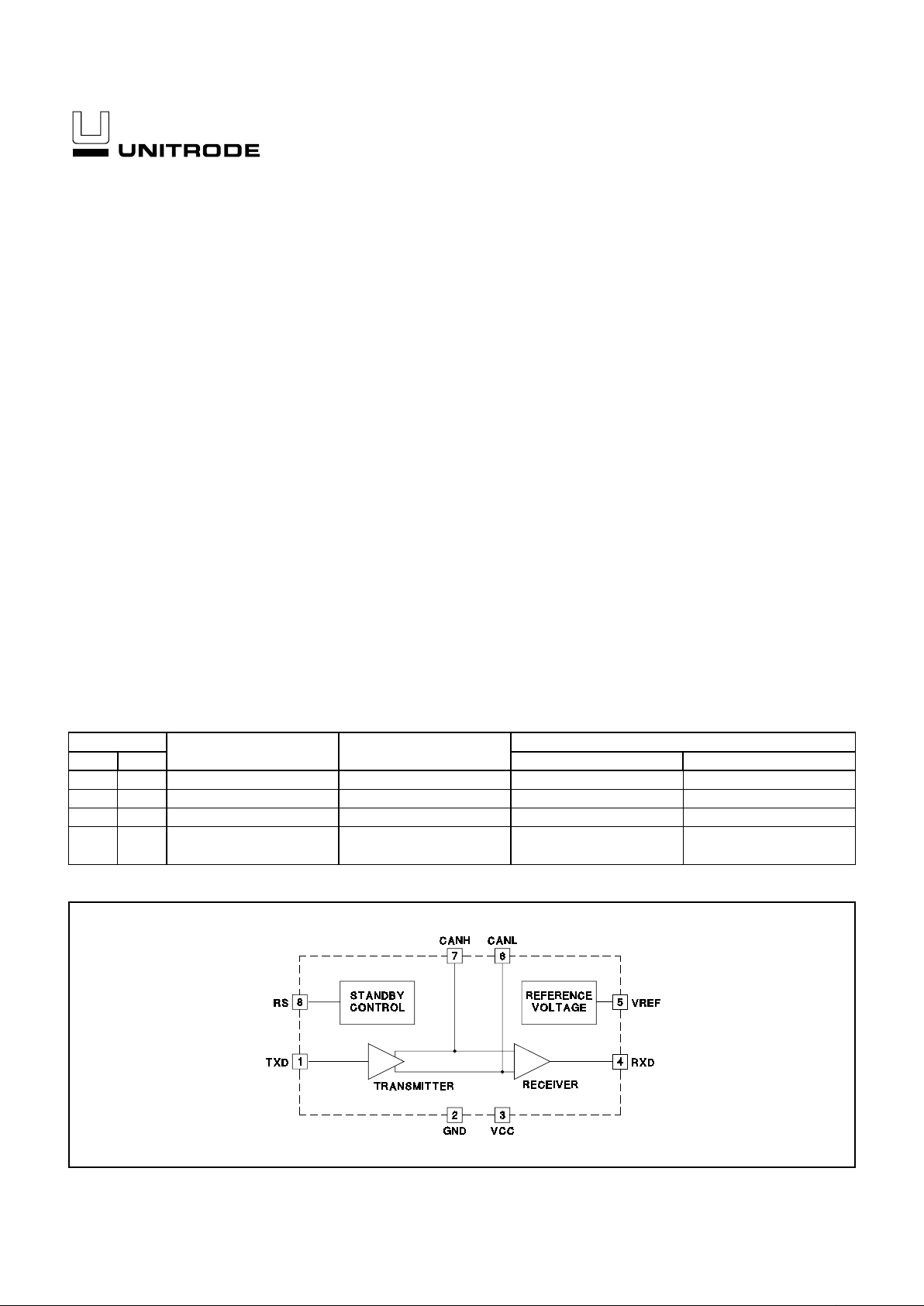
BLOCK DIAGRAM
FEATURES
•
Pin Compatible with PCA82C250
and DeviceNet, SDS, ISO11898
Compatible
•
High Speed, up to 1Mbps
•
Differential Transmit to the Bus and
Receive from the Bus to the CAN
Controller
•
At Least 110 Nodes Can Be
Connected
•
100V Transient Protection on the
Transmit Output
•
24V Supply Cross Wire Protection
on CANH and CANL
•
No Bus Loading When Powered
Down
• Operates over –40°C to +85°C
• Unitrode DeviceNet ID#107
CAN Transceiver
UDG-96202
DESCRIPTION
The UC5350 Control Area Network Transceiver is designed for industrial
applications employing the CAN serial communications physical layer
per ISO 11898 standard. The device is a high speed transceiver de
-
signed for use up to 1Mbps. Especially designed for hostile environ
ments, this device features cross wire, loss of ground, over voltage, and
over temperature protections well as a wide common mode range.
The transceiver interfaces the single ended CAN controller with the dif
ferential CAN bus found in industrial and automotive applications. It op
erates over the –7V to +12V common mode range of the bus and will
withstand common mode transients of –25V to +18V as well as Schaff
ner tests. Performance features include high differential input imped
ance, a symmetrical differential signal driver and very low propogation
delay that improves bus bandwidth and length by reducing reflection and
distortion.
The transceiver operates over a wide temperature range, –40°C to
+85°C and is available in 8-pin SOIC and Dual-in-Line packages.
Inputs System Mode Output Mode Outputs
TXD RS V
CANH -VCANL RXD
0 0 High Speed Dominant 1.5V to 3V 0
1 0 High Speed Recessive –120mV to +12mV 1
High Z 0 High Speed Recessive –120mV to +12mV 1
X 1 Standby High Z 0 at Bus = Dominant
1 at Bus = Recessive
FUNCTIONAL TABLE (VCC = 4.5V to 5.5V)
2
UC5350
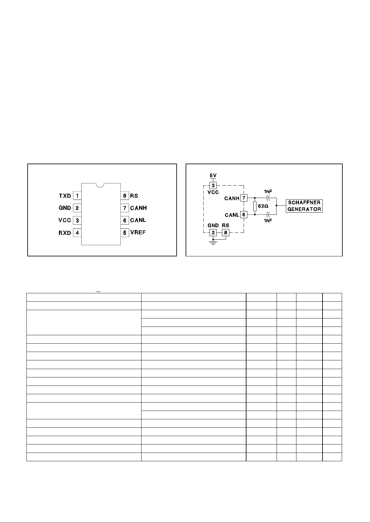
CONNECTION DIAGRAM
DIL-8, SOIC-8 (Top View)
N, D Package
ABSOLUTE MAXIMUM RATINGS
Supply Voltage . . . . . . . . . . . . . . . . . . . . . . . . . . . . –0.3V to 9V
TXD, RXD, VREF, RS . . . . . . . . . . . . . . . –0.3V to VCC + 0.3V
CANL, CANH
0V < VCC < 5.5V. . . . . . . . . . . . . . . . . . . . . . . . –8V to +36V
Non-Destructive, Non-Operative. . . . . . . . . . . . –8V to +32V
Transient, Schaffner Test (Fig. 1) . . . . . . . . . –150 to +100V
Operating Temperature . . . . . . . . . . . . . . . . . . –40°C to +85°C
Storage Temperature . . . . . . . . . . . . . . . . . . . –65°C to +150°C
Junction Temperature. . . . . . . . . . . . . . . . . . . –55°C to +150°C
Lead Temperature (Soldering, 10 sec.). . . . . . . . . . . . . +300°C
Crosswire Protection Maximum VBUS . . . . . . . . . . . . . . . . 30V
Bus Differential Voltage* . . . . . . . . . . . . . . . . . . . . . . . . . . . 30V
Cross Wire Protection T
A. . . . . . . . . . . . . . . . . –40°C to 125°C
ELECTRICAL CHARACTERISTICS (Total Device) Unless otherwise stated, the device is disconnected from the bus
line; VCC = 4.5V to 5.5V; 60
in parallel with 100pF load between CANH and CANL; TA = –40°C to +85°C, TA=T
J
PARAMETER TEST CONDITIONS MIN TYP MAX UNITS
Supply Voltage 4.5 5.5 V
Supply Current Dominant, TXD = 1V 70 mA
Recessive, TXD = 4V 9 14 mA
Standby, RS = 4V 1.2 2.0 mA
RS Input Current –10 5 µA
RS Voltage Input = Logic 1 Standby 0.75VCC V
RS Voltage Input = Logic 0 High Speed 0.3VCC V
Transmitter Voltage Input = Logic 1 Transmitter Output Recessive 0.7VCC V
Transmitter Voltage Input = Logic 0 Transmitter Output Dominant 0.3VCC V
Transmitter Current Input at Logic 1 TXD = 4V 30 µA
Transmitter Current Input at Logic 0 TXD = 1V –30 30 µA
Receiver Voltage Output = Logic 1 RXD = –100µA, TXD = 4V VCC –1.25 V
Receiver Voltage Output = Logic 0 RXD = 1mA, TXD = 1V 0.75 1.2 V
RXD = 10mA, TXD = 1V 1.2 1.7 V
CANH, CANL Input Resistance No Load, TXD = 4V 20 40 kΩ
Differential Input Resistance No Load, TXD = 4V 40 80 kΩ
CANH, CANL Input Capacitance (Note 1) 20 pF
Differential Input Capacitance (Note 1) 10 pF
Reference Output Voltage VREF = ±50µA 0.45VCC 0.55VCC V
Note 1: Guaranteed by design.Not 100% tested in production.
See Figure 7 for Pulse Timing
Figure 1. Schaffner Test
UDG-96203-1
Currents are positive into, negative out of the specified
terminal.
Consult Packaging Section of the Databook for thermal
limitations and considerations of packages.
*Refers to Figures 9, 10, 11, 12 and 13.

3
UC5350
ELECTRICAL CHARACTERISTICS (DC Parameters For Recessive State)
Unless otherwise stated, the
device is disconnected from the bus line; 60Ω in parallel with 100pF load between CANH and CANL.
PARAMETER TEST CONDITIONS MIN TYP MAX UNITS
V
CANH, VCANL No Load, TXD = 4V (Figure 2) 2 2.5 3 V
Differential Output Transmitter
(V
CANH – VCANL)
No Load, TXD = 4V (Figure 2) –500 0 50 mV
Differential Input Receiver Common Mode Range = –7V to +12V,
TXD = 4V, CANH, CANL Externally Driven
(Figure 3)
–1 0.40 V
Differential Input Resistance No Load 40 kΩ
CANH, CANL Input Resistance 20 kΩ
Figure 2. Recessive State Voltage Diagram
Figure 3. Recessive State Voltage Diagram
Valid output ofCANH, CANL during recessive state transmis
-
sion. TXD = LOGIC 1
UDG-96204
UDG-96205
Valid voltage range of V
CANH
for sensing dominant bus state
as V
CANL
varies over bus common range mode.
TXD = LOGIC1

4
UC5350
0.5V
2.25V
2.75V
3.5V
4.5V
5V
RANGE OF VCANH (SHADED)
VCANH (MAX)
V
CANH (MIN)
VCANL (MIN)
VCANL (MAX)
∆ V6,7 =1.5V (MIN)
∆ V6,7 =3V (MAX)
Figure 4. Dominant State Voltage Diagram
—7V
—2V
0V
—
6.1V
12V
BUS CMR (MAX)
V
CANL
5V
BUS CMR (MIN)
V
CANH
VDIFF(D) = 0.9V (MIN)
VDIFF(D) = 5V(MAX)
Figure 5. Dominant State Voltage Diagram
Valid voltage range of V
CANH
for sensing dominant bus state
as V
CANL
varies.TXD = LOGIC 0
UDG-97161
Valid voltage range of V
CANH
for sensing dominant bus
state as V
CANL
varies over bus common mode range.
TXD = LOGIC 0
ELECTRICAL CHARACTERISTICS (DC Parameters For Dominant State) Unless otherwise stated, the device
is disconnected from the bus line; 60 in parallel with 100pF load between CANH and CANL. VCC = 4.5V to 5.5V
PARAMETER TEST CONDITIONS MIN TYP MAX UNITS
CANH Output Voltage (V
CANH) TXD = 1V (Figure 4) 2.75 4.5 V
CANL Output Voltage (V
CANL) TXD = 1V (Figure 4) 0.50 1.1 2.25 V
Differential Output Transmitter (V
CANH -VCANL) TXD = 1V (Figure 4) 1.5 2 3 V
Differential Input Receiver (V
DIFF(D)) Common Mode Range = –2 to +7V, TXD = 4V,
CANH, CANL Externally Driven (Figure 5)
0.9 5 V
Common Mode Range = –7 to +12V, TXD = 4V,
CANH, CANL Externally Driven (Figure 5)
1.0 5 V
UDG-97160
TRANSMITTER CHARACTERISTICS
Unless otherwise stated, the device is disconnected from the bus line; 60Ω in
parallel with 100pF load between CANH and CANL.
PARAMETER TEST CONDITIONS MIN TYP MAX UNITS
Differential Output Transmitter
(V
CANH -VCANL)
Dominant Mode 1.5 2 3 V
Recessive Mode –500 50 mV
Delay From TXD to Bus Active T
ON (TXD) (Figure 6) 50 100 ns
Delay From TXD to Bus Inactive T
OFF (TXD) 60Ω Across CANH and CANL (Figure 6) 20 110 ns

5
UC5350
RECEIVER CHARACTERISTICS
Unless otherwise stated, the device is disconnected from the bus line; 60Ω in
parallel with 100pF load between CANH and CANL.
PARAMETER TEST CONDITIONS MIN TYP MAX UNITS
Differential Input Receiver (V
CANH - VCANL) Dominant Mode, TXD = 4V 0.9 V
Recessive Mode, TXD = 4V 0.4 V
Differential Input Hysteresis TXD = 4V 75 150 mV
Delay From Bus to RXD (T
ON) Inactive to Active Bus (Figure 6) 60 100 ns
Delay From Bus to RXD (T
OFF) Active to Inactive Bus, 60Ω Across CANH and
CANL (Figure 6)
80 115 ns
Figure 6. Transceiver AC Response
UDG-96208
Figure 7. Timing Diagram for Schaffner Tests
UDG-96209
Magnitude Specifications for VS
ISO DIN 40839-1 Schaffner
DP7637/1 (Draft) NSG500C/506C
Up to 150V Up to 150V 40V to 200V
TRANSCEIVER CHARACTERISTICS
PARAMETER TEST CONDITIONS MIN TYP MAX UNITS
Loop Time T
ON
(TXD) + TON(RXD) Inactive to active bus 110 200 ns
T
OFF
(TXD) + T
OFF
(RXD) Active to inactive bus 100 225 ns

6
UC5350
UNITRODE CORPORATION
7 CONTINENTAL BLVD.• MERRIMACK, NH 03054
TEL. (603) 424-2410 • FAX (603) 424-3460
3
INPUT
7
VCC
6
2
GND
78L05
+VBUS
CANH
CANL
CANH
CANL
60Ω
GND
OUTPUT
Figure 8. Normal Connection
3
INPUT
7
VCC
6
2
GND
78L05
+VBUS
CANH
CANL
CANH
CANL
60Ω
GND
OUTPUT
Figure 9. Crosswire No. 1
3
INPUT
7
VCC
6
2
GND
78L05
+VBUS
CANH
CANL
CANH
CANL
60Ω
GND
OUTPUT
Figure 10. Crosswire No. 2
3
INPUT
7
VCC
6
2
GND
78L05
+VBUS
CANH
CANL
CANL
CANH
60Ω
GND
OUTPUT
Figure 11. Crosswire No. 3
3
INPUT
7
VCC
6
2
GND
78L05
+VBUS
CANH
CANL
CANH
CANL
60Ω
GND
OUTPUT
Figure 12. Crosswire No. 4
3
INPUT
7
VCC
6
2
GND
78L05
+VBUS
CANH
CANL
CANH
CANL
60Ω
GND
OUTPUT
Figure 13. Crosswire No. 5
 Loading...