

Octal Line Receiver
FEATURES
• Meets EIA232E/423A/422A and CCITT
V.10, V.11, V.28, X.26, X.27
• Single +5V Supply—TTL Compatible
Outputs
• Differential Inputs withst and ±25V
• Low Open Circuit Voltage for Improved
Failsafe Characteristic
• Reduced Supply Current—35mA Max
• Internal Hysteresis
DESCRIPT ION
The UC5181C is an octal line receiver designed to meet a wide range
of digital communications requirements as outlined in EIA standards
EIA232E, EIA422A, EIA423A and CCITT V.10, V.11, V.28, X.26, and
X.27. The UC5181C is similar to the UC5180C, but without the input
filtering. Thus, it covers the entire range of data rates up to 10MBPS. A
failsafe function allows these devices to “fail” to a known state under a
wide variety of fault conditions at the inputs.
ABSOLUTE MAXI MUM RATING S (Note 1)
Supply Voltage, V
CC . . . . . . . . . . . . . . . . . . . . . . . . . . . . . . . . . . . . . . . . . . . . 7V
Output Sink Current. . . . . . . . . . . . . . . . . . . . . . . . . . . . . . . . . . . . . . . . . . 50mA
Output Short Circu it Tim e . . . . . . . . . . . . . . . . . . . . . . . . . . . . . . . . . . . . . 1 Sec
Common Mode Input Range. . . . . . . . . . . . . . . . . . . . . . . . . . . . . . . . . . . . . 15V
Differ enti al In put R ange . . . . . . . . . . . . . . . . . . . . . . . . . . . . . . . . . . . . . . . . 25V
Failsafe Voltage. . . . . . . . . . . . . . . . . . . . . . . . . . . . . . . . . . . . . . . . . -0.3 to V
CC
PLCC Power Dissipation , TA=25° C (Note 2). . . . . . . . . . . . . . . . . . . 1000 m W
DIP Power D issipat ion, T
A=25° C (Not e 2). . . . . . . . . . . . . . . . . . . . . 1200 mW
Storag e Temperatur e Range . . . . . . . . . . . . . . . . . . . . . . . . -65° C to +150° C
Lead Temp era ture (Solder ing, 10 seconds). . . . . . . . . . . . . . . . . . . . . . -300° C
Note 1: All voltages are with respec t to ground , pin 14. Current s are posit ive in,
negative out of the specif ied terminal.
Note 2: Consult packaging section of Databoo k for ther mal limitations an d
consideration s of packa ge.
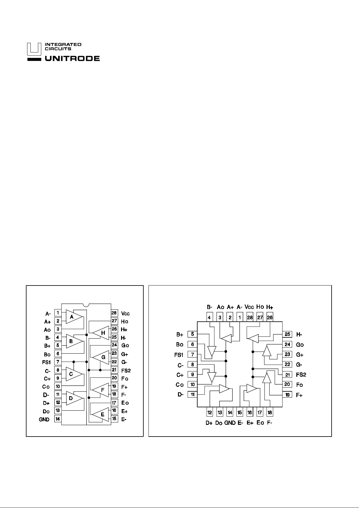
CONNECTION DIAGRAMS
UC5181C
DIL-28 (TOP VIEW) PLCC-28 (TOP VIEW)
1/94
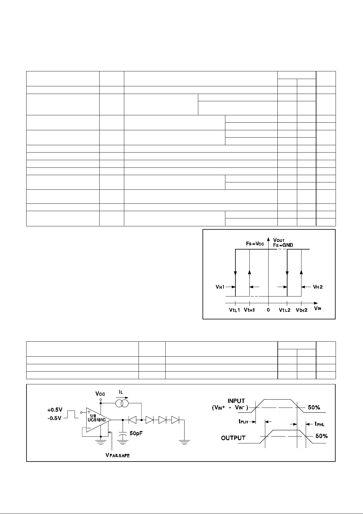
DC ELECTRICAL CHARACTERI STICS:
PARAMETER SYMBOL TEST CONDITIONS UC5181C UNITS
MIN MAX
DC Input Resistance R
IN 3V ≤ |VIN|≤25V 3 7 kΩ
Failsafe Output Voltage V
OFS Input s Open or Shorted
Together, or One Input Open
and One Grounded
0≥IOUT≤8mAVFAILSAFE=0V 0.45 V
0≥I
OUT≥-400µA, VFAILSAFE=VCC
2.7
Differential In put High
Threshold
V
TL VOUT= 0.45V, IOUT = -440µA (See Figure
1)
RS = 0 (Note 3) 50 200 mV
R
S = 500 (Note 3) 400
Differential In put Low
Threshold
V
TL VOUT = 0.45V, IOUT = 8 mA (See Figure
1)
RS = 0 (Note 3) -200 -50 mV
R
S = 500 (Not e 3) -400
Hysteresis V
H FS=0V or VCC (See Figure 1) 45 140 mV
Open Circuit Input Voltage V
IOC 75 mV
Input Capacita nce C
I 20 pF
High Level Output Voltage V
OH
VID = 1V, IOUT = -440 µA2.7V
Low Level Output Volta ge V
OL
VID = -1V (Note 4)
I
OUT = 4 mA 0.4 V
I
OUT = 8 mA 0.45
Short Circuit Output
Current
I
OS Note 5 20 100 mA
Supply current I
CC 4.75V ≤VCC≤5.25V 35 mA
Input Curren t I
IN
Other Inputs Grounded
V
IN = +10V 3.25 mA
V
IH = -10V -3.25
PARAMETER SYMBOL TEST CONDITIONS UC5181C UNITS
MIN MAX
Propagation Delay–Low to High t
PLH CL=50pF, VIN=
±
500 mV (Note 6) 120 ns
Propagation Dela y–High to Low t
PHL CL=50pF, VIN=
±
500 mV (Note 6) 120 ns
Acceptable Input f requenc y f
A Unused Input Grounded, VIN=
±
200 mV 5.0 MHz
Note 3: RS is a resistor in series with each input.
Note 4: Measur e aft er 10 0 ms wa rm up (a t 0
°
C).
Note 5: Only 1 output may be sh ort ed at a time and t hen on ly for a
maximum of 1 sec.
Note 6: The delays, eith er t
PLH
or t
PHL
, shall not var y from receiver to
receiver by more than 35ns.
Figure 2. AC Te st Circuit
AC ELECTRICAL CHARACTERIST ICS :
Figure 1. VTL, VTH,VH Definition
UC5181C
Unless otherwise st ated, these specif icat ions apply fo r TA = 0°C to +70°C; VCC
= 5V ±5%, Input Common Mode Range ±7V, TA=TJ.
VCC=5V ±5%. TA=0°C to +70°C, Figur e 2 TA=TJ.
2

APPLICATIONS INFORMATION
Failsafe Operati on
These devices provide a failsafe operating mode to guard
against input fault condi tions as defined in EIA422A and
EIA423A standards. These fault conditions are (1) driver
in power-off condition, (2) receiver not interconnected
with driver, (3) open-circuited interconnecting cable, and
(4) short-circuited interco nnecting cable. If one of these
four fault conditions occurs at the inputs of a receiver,
then the output of that receiver is driven to a known logic
level. The re ceive r is progra mmed by co nnecting the failsafe input to V
CC or ground. A connection to VCC provides
a logic “1 " outpu t under fau lt conditi ons, whil e a connection to grou nd p rovid es a logic ”0 " . The re are two failsafe
pins (F
S1 and FS2) on the UC5181C where each provides
common failsafe control for four receivers.
EIA232E/V.28 / EIA423A/V.10 DATA TRANSMISSION
EIA422A/V.11 DA TA TRANSMISSION
UC5181C
UNITRODE INTEGRATED CIRCUITS
7 CONTINENTAL BLVD. •• MERRIMACK, NH 03054
TEL. (603) 424-2410 •• FAX (603) 424-3460
GENERAL LAYO UT NOTE S
The drivers and receivers should be mounted close to the
system common ground point, with the ground reference
tied to the common point to reduce RFI/EMI.
Filter connectors or transzorbs should be used to reduce
the RFI/EMI, and protecting the system from static (ESD),
and electrical overstress (EOS). A filter connector or capacitor will reduce the ESD pulse by 90% typically. A cable dragged a cross a carpet an d connected to a system
can easily be charged to over 25,000 volts. This is a metal to metal contact when the cab le is connected to the
system (no resistance), currents exceed 80 amps with
less than a nanosecond rise time. A transzorb provides
two functions, the device capacitance inherently acts as a
filter capacitor, and the device clamps the ESD and EOS
pulses which would pass through the capacitor and destroy the devices. The recommended transzorb for the
UC5180C and the UC5181C is P6KE22CA.
* Transzorb is a trademark of General Semiconductor
Industries.
EIA423A/V.10
3

IMPORTANT NOTICE
T exas Instruments and its subsidiaries (TI) reserve the right to make changes to their products or to discontinue
any product or service without notice, and advise customers to obtain the latest version of relevant information
to verify, before placing orders, that information being relied on is current and complete. All products are sold
subject to the terms and conditions of sale supplied at the time of order acknowledgement, including those
pertaining to warranty, patent infringement, and limitation of liability.
TI warrants performance of its semiconductor products to the specifications applicable at the time of sale in
accordance with TI’s standard warranty. Testing and other quality control techniques are utilized to the extent
TI deems necessary to support this warranty. Specific testing of all parameters of each device is not necessarily
performed, except those mandated by government requirements.
CERT AIN APPLICATIONS USING SEMICONDUCTOR PRODUCTS MAY INVOLVE POTENTIAL RISKS OF
DEATH, PERSONAL INJURY, OR SEVERE PROPERTY OR ENVIRONMENTAL DAMAGE (“CRITICAL
APPLICATIONS”). TI SEMICONDUCTOR PRODUCTS ARE NOT DESIGNED, AUTHORIZED, OR
WARRANTED TO BE SUITABLE FOR USE IN LIFE-SUPPORT DEVICES OR SYSTEMS OR OTHER
CRITICAL APPLICATIONS. INCLUSION OF TI PRODUCTS IN SUCH APPLICA TIONS IS UNDERSTOOD T O
BE FULLY AT THE CUSTOMER’S RISK.
In order to minimize risks associated with the customer’s applications, adequate design and operating
safeguards must be provided by the customer to minimize inherent or procedural hazards.
TI assumes no liability for applications assistance or customer product design. TI does not warrant or represent
that any license, either express or implied, is granted under any patent right, copyright, mask work right, or other
intellectual property right of TI covering or relating to any combination, machine, or process in which such
semiconductor products or services might be or are used. TI’s publication of information regarding any third
party’s products or services does not constitute TI’s approval, warranty or endorsement thereof.
Copyright 1999, Texas Instruments Incorporated

IMPORTANT NOTICE
T exas Instruments and its subsidiaries (TI) reserve the right to make changes to their products or to discontinue
any product or service without notice, and advise customers to obtain the latest version of relevant information
to verify, before placing orders, that information being relied on is current and complete. All products are sold
subject to the terms and conditions of sale supplied at the time of order acknowledgement, including those
pertaining to warranty, patent infringement, and limitation of liability.
TI warrants performance of its semiconductor products to the specifications applicable at the time of sale in
accordance with TI’s standard warranty. Testing and other quality control techniques are utilized to the extent
TI deems necessary to support this warranty. Specific testing of all parameters of each device is not necessarily
performed, except those mandated by government requirements.
CERT AIN APPLICATIONS USING SEMICONDUCTOR PRODUCTS MAY INVOLVE POTENTIAL RISKS OF
DEATH, PERSONAL INJURY, OR SEVERE PROPERTY OR ENVIRONMENTAL DAMAGE (“CRITICAL
APPLICATIONS”). TI SEMICONDUCTOR PRODUCTS ARE NOT DESIGNED, AUTHORIZED, OR
WARRANTED TO BE SUITABLE FOR USE IN LIFE-SUPPORT DEVICES OR SYSTEMS OR OTHER
CRITICAL APPLICATIONS. INCLUSION OF TI PRODUCTS IN SUCH APPLICA TIONS IS UNDERSTOOD T O
BE FULLY AT THE CUSTOMER’S RISK.
In order to minimize risks associated with the customer’s applications, adequate design and operating
safeguards must be provided by the customer to minimize inherent or procedural hazards.
TI assumes no liability for applications assistance or customer product design. TI does not warrant or represent
that any license, either express or implied, is granted under any patent right, copyright, mask work right, or other
intellectual property right of TI covering or relating to any combination, machine, or process in which such
semiconductor products or services might be or are used. TI’s publication of information regarding any third
party’s products or services does not constitute TI’s approval, warranty or endorsement thereof.
Copyright 2000, Texas Instruments Incorporated
 Loading...