

ABSOLUTE MAXIMUM RATINGS (Note 1)
Supply Voltage, VCC . . . . . . . . . . . . . . . . . . . . . . . . . . . . . . . . . . . . . . . . . . . 7V
Output Sink Current. . . . . . . . . . . . . . . . . . . . . . . . . . . . . . . . . . . . . . . . . 50 mA
Output Sho rt C ircuit Time . . . . . . . . . . . . . . . . . . . . . . . . . . . . . . . . . . . . . 1 Sec
Common Mo de Inpu t Ra nge. . . . . . . . . . . . . . . . . . . . . . . . . . . . . . . . . . . . 15V
Differential I nput Range. . . . . . . . . . . . . . . . . . . . . . . . . . . . . . . . . . . . . . . . 25V
Failsafe Voltage. . . . . . . . . . . . . . . . . . . . . . . . . . . . . . . . . . . . . . . . . -0.3 to V
CC
PLCC Power Dissipation, TA = 25°C (Note 2). . . . . . . . . . . . . . . . . . . 1000 mW
DIP Power Dissipation, T
A = 25°C (Note 2) . . . . . . . . . . . . . . . . . . . . 1200 mW
Storage Temp era ture Ran ge. . . . . . . . . . . . . . . . . . . . . . . . . . -65°C to +150°C
Lead Temperatur e (So ldering , 10 Second s). . . . . . . . . . . . . . . . . . . . . . -300°C
Note 1: All voltages are with respect to ground, pin 14. Curren ts are positive
into, negative out of the specif ied t erminal
Note 2: Consult Packa ging Section of Databo ok for ther mal limitations and
considerations of package.
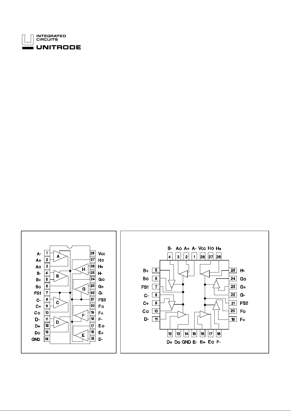
Octal Line Receiver
UC5180C
DIL-28 (TOP VIEW)
CONNECTION DIAGRAMS
DESCRIPTION
The UC5180C is an octal l ine receiver designed t o meet a wide range
of digital communications requiremen ts as outlined in EIA standards
EIA232E, EIA423A, EIA422A, and CCITT V.10, V.11, V.28, X.26, and
X.27. The UC5180C includes an input noise filter and is intended for
applications e mployi ng data rates up to 200 KBPS. A failsafe function
allows these de vices to "fail " to a known state under a wide variety of
fault conditions at the inputs.
FEATURES
• Meets EIA 232E/423A/422A and CCITT
V.10,V.11, V.28, X.26, X.27
• Single +5V Supply--TTL Compatible
Outputs
• Differential Inputs Withstand ± 25V
• Low Open Circuit Voltage for Improved
Failsafe Characteristi c
• Reduced Supply Current--35 mA Max
• Input Noise Filter
• Internal Hysteresis
PLCC-28 (TOP VIEW)
1/94
DC ELECTRICAL CHARACTERISTI CS:
PARAMETERS SYMBOL TEST CONDITIONS UC5180C UNITS
MIN MAX
DC Input Resistance R
IN 3V ≤ | VIN | ≤ 25V 3 7 kΩ
Failsafe Output Voltage V
OFS Input s Open or Shorted
Together, or One Input
Open and One Grounde d
0 ≤ IOUT ≤ 8mA, VFAILSAFE = 0V 0.45 V
0 ≥ I
OUT ≥ - 400 µA,
V
FAILSAFE = VCC
2.7
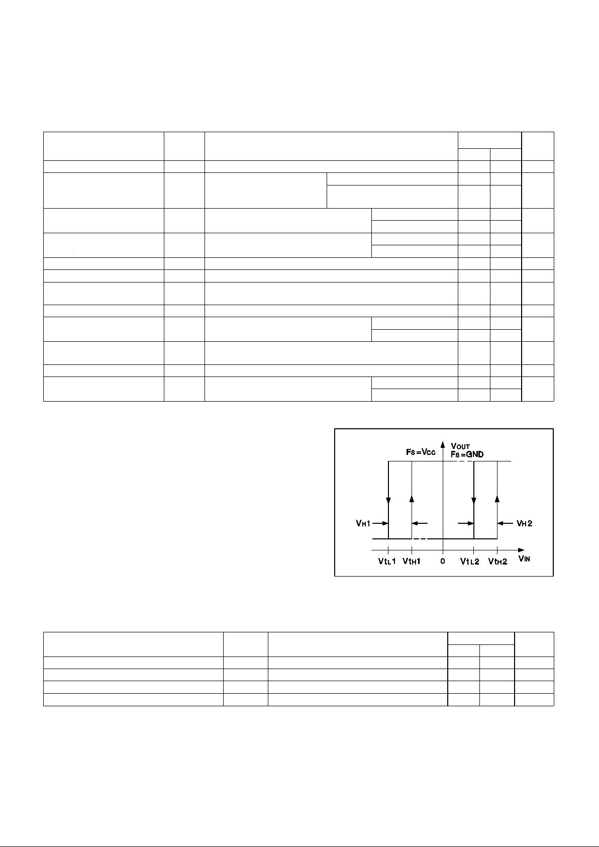
Differential In put High
Threshold
V
TH VOUT = 2.7V, IOUT = 440 µA
(See Figure 1)
RS = 0 (Note 2) 50 20 0 mV
R
S = 500 (Note 2) 400
Differential In put Low
Threshold
V
TL VOUT = 0.4 5V, IOUT = 440 mA
(See Figure 1)
RS = 0 (Note 2) -200 -5 0 mV
R
S = 500 (Note 2) -400
Hysteresis V
H FS = 0V or VCC (See Figure 1) 50 140 mV
Open Circuit Input Voltage V
ICC 75 mV
Input Capacita nce C
I 20 pF
High Level Output Voltage V
CH VID = 1V, IOUT = - 440 µ A2.7V
Low Level Output Volta ge V
OL VID = -1V
(Note 3)
IOUT = 4 mA 0.4 V
I
OUT = 8 mA 0.45
Short Circuit Output
Current
I
OS Note 4 20 100 mA
Supply Current I
CC 4.75V ≤ VCC ≤ 5.25V 35 mA
Input Curren t I
IN Other Inputs Grounded VIN = +10V 3.25 mA
V
IN
= -10V -3.25
UC5180C
Figure 1. VtL, VtH, VH Def inition
Unless otherwise stated these specifica tion s apply for TA = 0°C to +70°C, V CC
= 5V ± 5%, Input Common Mod e Range ± 7V, TA =TJ
AC ELECTRICAL CHARACTERIS TI CS:
PARAMETERS SYMBOL TEST CONDITION S UC5180C UNITS
MIN MAX
Propagation Delay - Low to High t
PLH CL = 50pF, VIN =
±
500mV 550 ns
Propagation Dela y - High to Low t
PHL CL = 50pF, VIN =
±
500mV 550 ns
Acceptance Input Frequency f
A Unused I npu t Ground ed, VIN = ± 200mV 0.1 MHz
Rejectable Input Frequency f
R Unu sed Inpu t Ground ed, VIN = ± 500m V 5.5 MHz
V
CC = 5V ± 5%, TA = 0°C to + 70°C, Figure 2, TA = TJ.
Note 2: RS is a resistor in series with each input.
Note 3: Measured after 100ms warm up (at 0°C)
Note 4: Only 1 output may be shorted at one time
and then only for a maximum of 1 sec.
2

UC5180C
APPLICATIONS INFORMATION
Failsafe Operati on
These devices provide a failsafe operating mode to
guard against input fault conditions as defined in
EIA422A and EIA423A standards. These fault conditions are (1) drive in power-off condition, (2) receiver not
interconnected with driver, (3) open-circuited interconnecting cable, and (4) short-circuited interconnecting
cable. If one of these fou r fa ult con diti ons occurs at the
inputs of a recei ver, then the output o f that receiver is
driven to a known logic level. The receiver is programmed by connecting the failsafe input to V
CC or
ground. A connection to V
CC provides a logic "1" output
under fault conditions, while a connection to ground
provides a logic "0". There are two failsafe pins (F
S1
and FS2) on the UC5180C where each provides common failsafe control for four receivers.
Input Filtering (UC5180C)
The UC5180C h a s in put filtering for additional noise rejection. This filtering is a function of both signal level
and frequency. For the specified input (5.5 MHz at ±500
mV) the input stage filter attenuates the signal such that
the output stage threshold level s are not exceeded and
no change of state occurs at the output.
EIA232E/V.28 / EIA423A/V.10 DATA TRANSMISSION
EIA422A/V.11 DATA TRANSMISSION
UNITRODE INTEGRATED CIRCUITS
7 CONTINENTAL BLVD. •• MERRIMACK, NH 03054
TEL. (603) 424-2410 •• FAX (603) 424-3410
Figure 2. AC Test Circuit
3

IMPORTANT NOTICE
T exas Instruments and its subsidiaries (TI) reserve the right to make changes to their products or to discontinue
any product or service without notice, and advise customers to obtain the latest version of relevant information
to verify, before placing orders, that information being relied on is current and complete. All products are sold
subject to the terms and conditions of sale supplied at the time of order acknowledgement, including those
pertaining to warranty, patent infringement, and limitation of liability.
TI warrants performance of its semiconductor products to the specifications applicable at the time of sale in
accordance with TI’s standard warranty. Testing and other quality control techniques are utilized to the extent
TI deems necessary to support this warranty. Specific testing of all parameters of each device is not necessarily
performed, except those mandated by government requirements.
CERT AIN APPLICATIONS USING SEMICONDUCTOR PRODUCTS MAY INVOLVE POTENTIAL RISKS OF
DEATH, PERSONAL INJURY, OR SEVERE PROPERTY OR ENVIRONMENTAL DAMAGE (“CRITICAL
APPLICATIONS”). TI SEMICONDUCTOR PRODUCTS ARE NOT DESIGNED, AUTHORIZED, OR
WARRANTED TO BE SUITABLE FOR USE IN LIFE-SUPPORT DEVICES OR SYSTEMS OR OTHER
CRITICAL APPLICATIONS. INCLUSION OF TI PRODUCTS IN SUCH APPLICA TIONS IS UNDERSTOOD T O
BE FULLY AT THE CUSTOMER’S RISK.
In order to minimize risks associated with the customer’s applications, adequate design and operating
safeguards must be provided by the customer to minimize inherent or procedural hazards.
TI assumes no liability for applications assistance or customer product design. TI does not warrant or represent
that any license, either express or implied, is granted under any patent right, copyright, mask work right, or other
intellectual property right of TI covering or relating to any combination, machine, or process in which such
semiconductor products or services might be or are used. TI’s publication of information regarding any third
party’s products or services does not constitute TI’s approval, warranty or endorsement thereof.
Copyright 1999, Texas Instruments Incorporated
 Loading...