

UC5170C
FUNCTIONAL TABLE
INPUTS OUTPUTS
HIGH LOW
EN DATA EIA-232E
(2)
EIA423A+EIA232E
0 0 (V+)-3V 5V to 6V
0 1 (V-)-3V −5V to -6V
1 X High Z High Z
Note 2: Minimum output swings.
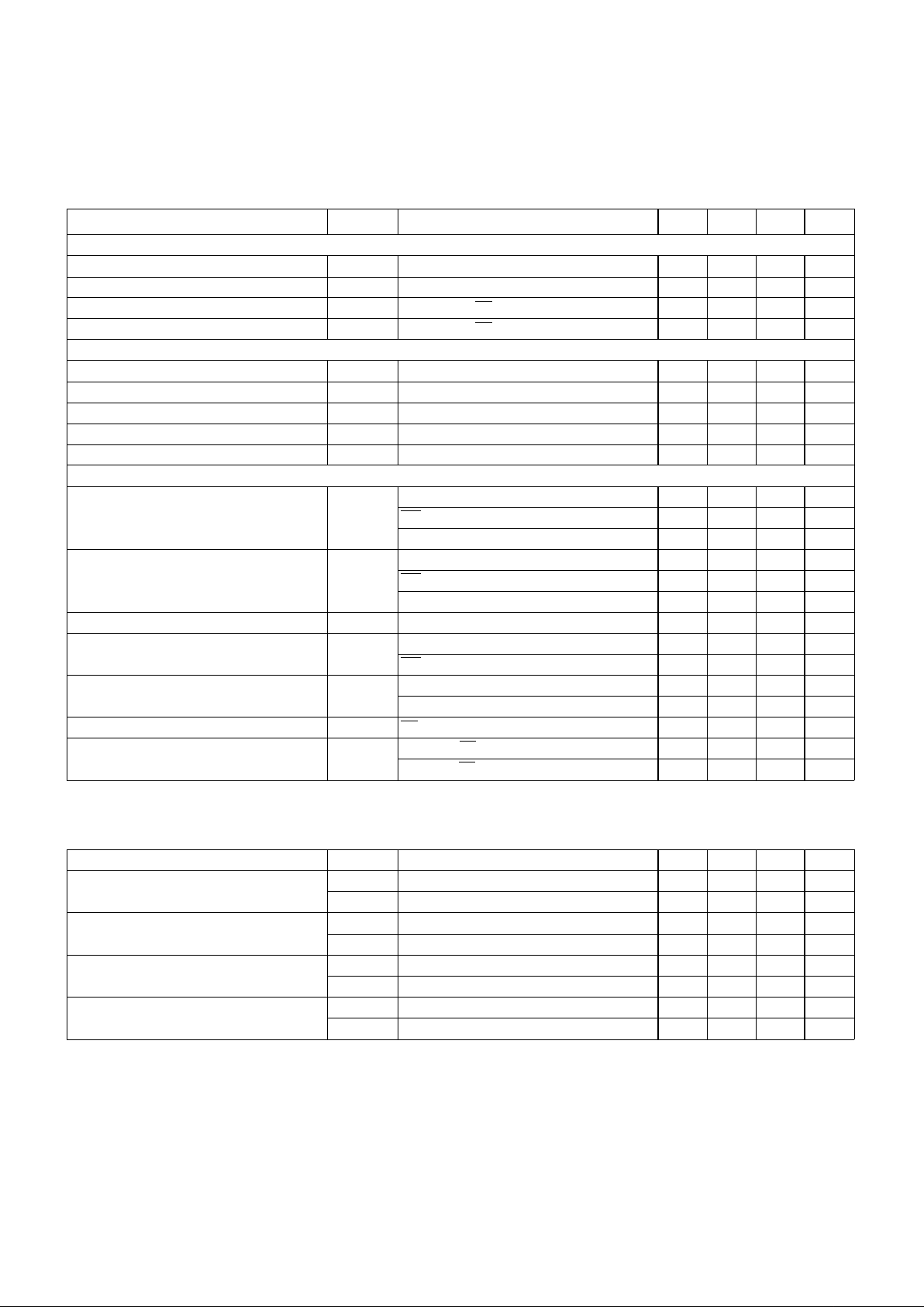
N PACKAGE (TOP VIEW)
Q PACKAGE (TOP VIEW)
Octal Line Driver
FEATURES
• Eight Single Ended Line Drivers in
One Package
• Meets EIA Standards
EIA232E/V.28, EIA423A and
CCITT V.10/X.26
• Single External Resistor Controls
Slew Rate
• Wide Supply Voltage Range
• Tri-State Outputs
• Output Short-Circuit Prot ect ion
DESCRIPTI ON
The UC5170C is a single-ended octal line driver designed to meet both
standard mod em control applicati ons (EIA232E/V.28), and long line drive
applications (EIA423A/V.10/X.26). The slew rate for all eight drivers is controlled by a single external resistor. The slew rate and o utput levels in Low
Mode are independent of the power variations.
Mode selection is easi ly accomplished by taking the select pins (M
S+ and
M
S-) to ground for low output mode (EIA232E/V.28 and EIA423A/V.10) or
to their respective supplies for high mode (EIA232E/V.28). High mode
should only by used to drive adapters that take power from the control
lines, or applications using high threshold receivers.
ABSOLUTE MAXI MUM RATING S (Not e 1)
V+ (Pin 20) . . . . . . . . . . . . . . . . . . . . . . . . . . . . . . . . . . . . . . 15V
V- (Pin 11). . . . . . . . . . . . . . . . . . . . . . . . . . . . . . . . . . . . . . −15V
PLCC Power Dissipation , T
A = 25 ° C (Not e 2 ) . . . . . . 1 000 mW
DIP Power Dissipat ion, T
A = 25°C (Note 2). . . . . . . . 1250 mW
Input Voltag e. . . . . . . . . . . . . . . . . . . . . . . . . . . . . −1.5V t o +7V
Output Voltage . . . . . . . . . . . . . . . . . . . . . . . . . . . −12V to +12V
Slew Rate Resistor. . . . . . . . . . . . . . . . . . . . . . . . . . 2k to 10kΩ
Storage Temperature . . . . . . . . . . . . . . . . . . . −65°C to +150°C
Note 1: All volta ges ar e with respect to ground, pin 18.
Note 2: Consult Packag ing Section of Databoo k for ther mal limitations and considerat ions of pack ages .
CONNECTION DIAGRAMS
7/95
UC5170C
DC ELECTRICAL CHARACTERIST ICS :
PARAMETERS SYMBOL TEST CONDITIONS MIN TYP MAX UNITS
POWER SUPPLY REQUIREMENTS
V+ Range 915V
V- Range -9 -15 V
V+ Supply Current I+ R
L = Infinite En = 0V 25 42 mA
V- Supply Current I- RL = Infinite En = 0V -23 -42 mA
INPUTS
High Level Input Voltage V
IH 2.0 V
Low Level Input Voltage V
IL 0.8 V
Input Clamp Volta ge V
IK II = -15 mA -1.1 -1.8 V
High Level Input Current I
IH VIH = 2.4V 0.25 40 µA
Low Level Input Current I
IL VIL
= 0.4V -200 -8.0 µA
OUTPUTS
High Level (Low Mode) O utput Voltage V
OH VIN = 0.8V RL = Inf. 5.0 5.3 6.0 V
(EIA423A/V.10, EIA232E/V.28)
En = 0.8V RL = 3k 5.0 5.3 6.0 V
R
L = 450 4.5 5.2 6.0 V
Low Level (Low Mode) Output Volt age V
OL VIN = 2.0V RL = Inf. -5.0 -5.3 -6.0 V
(EIA423A/V.10,EIA232E/V.28)
En = 0.8V RL = 3k -5.0 -5.3 -6.0 V
R
L = 450 -4.5 -5.2 -6.0 V
Output Balance (EIA423A/V.10) V
BAL RL = 450 VOH - VOL = V BAL 0.2 0.4 V
High Level (High Mode) Output Volta ge V
OH VIN = 0.8V RL = Inf., MS+ = V+, MS- = V- 7.0 7.6 10 V
(EIA232E/ V.2 8) En = 0.8V RL = 3k, MS+ = V+, MS- = V- 7.0 7.6 10 V
Low Level (High Mode) Output Voltage V
OL VIN = 2.0V RL = Inf. , MS+ = V+, MS- =V- -7.0 -7.7 -10 V
(EIA232E, V.28) En = 0.8V R
L = 3k, MS+ = V+, MS- = V- -7.0 -7.7 -10 V
Off-Stat e O utput Current I
OZ En = 2.0V, VO =
±
6V, V+ = 15V, V- = -15V -100 100 µA
Short-Circuit Cur re nt I
OS VIN = 0V, En = 0V 25 50 mA
V
IN = 5V, En = 0V 25 40 mA
Unless otherwise stated these sp ecif icatio ns hold for | V+ | = | V - | = 10V,
0 < TA < +70°C, MS+ = MS− = 0V, RSRA = +10k, TA =TJ.
at | V+ | = | V - | = 10V, 0 < TA < +70°C, MS+ = MS− = 0V, TA =TJ.
PARAMETERS SYMBOL TEST CONDITIONS MIN TYP MAX UNITS
Output Slew Rate t
R RSRA = 2k 6.65 9 .5 12.3 V/µs
t
F RL = 450, CL = 50pF 6.65 10 12.3 V/µs
Output Slew Rate t
R RSRA = 10k 1.33 1.9 2.45 V/µs
t
F RL = 450, CL = 50pF 1.33 2.2 2.45 V/µs
Propagation Output to t
Hz RSRA = 10k 0.3 1 .0 µs
High Impedance t
Lz RL = 450, CL = 50pF 0. 5 1.0 µs
Propagation High Impedance to t
zH RSRA = 10k 6.0 15 µs
Output t
zL RL = 450, CL = 50pF 7.0 15 µs
AC ELECTRICAL CHARACTERIST ICS :
2

UC5170C
APPLICATION INF ORMATI ON
Slew Rate Programming
Slew rate for the UC5170C is set up by a single external
resistor connected between the SRA pin and ground.
Slew rate adjustments can be approximated by using
the following formula:
V
⁄ µs =
20
R
SRA
(R
SRA
in k
Ω)
The slew rate resistor can vary between 2k and 10k
which allows slew rates between 10 to 2.2V/µs, respectively. The relationship between slew rate and RSRA is
shown in the typical characteristics.
Waveshaping of the output lets the user control the
level of interference (near-end crosstalk) that may be
coupled to adjacen t circuits in an interconnection. The
recommended output characteristics for cable length
and data rates can be foun d in EIA standard EIA423A
+V.10. Approxi mations of these s tandards are given by
the following equations:
Max. Data Rate = 300/t (For data rates 1k to 100k bit/s)
Max. Cable Length (feet) = 100 x t (Max. length 4000 feet)
where t is the transition time from 10% to 90% of the
output swing in microseconds. For data rates below 1k
bit/s t may be up to 300 microseconds.
Output Voltage Programming
The UC5170C has two programmable output modes,
either a low voltage mode which meets EIA423A,
EIA232E/V.28/V.10 specifications, or the high output
mode which meets the EIA232E, V.28 specifications.
The high output mode provides greater output swings,
minimum of 3V below and supply rails for driving higher,
attenuated lines. This mode is selected by connecting
the mode select pins to their respected supplies, M
S+ to
V+ and M
S- to V- .
The low output mode provides a controlled output swing
and is accomplished by connecting both mode select
pins to ground.
AC PARAMETER TEST CIRCUIT AND WAVEFORMS
AC CHARACTERISTICS
Driver Slew Rate
Low Output Driver t
R & tF (10-90%)
EIA232E + EIA423A Mode
3

UC5170C
APPLICATIONS
UNITRODE INTEGRATED CIRCUITS
7 CONTINENTAL BLVD. • MERRIMACK, NH 03054
TEL. (603) 424-2410 • FAX (6 03) 424-3460
Filter connectors or transzorbs should be used to reduce
the RFI/EMI, protecting the system from static (ESD), and
electrical overstress (EOS). A filter connector or capacitor
will reduce the ESD pulse by 90% typically. A cable
dragged acro ss a carpet and connected to a system can
easily be cha rged to over 25,00 vol ts. This is a metal to
metal contact when the cable is connected to the system
(no resistance), currents exceed 80 amps with less than a
nanosecond rise time. A transzorb provides two functions,
the device capaci tance inherently acts a s a filter capacitor, and the device clamps the ESD and EOS pulses
which would pass through the cap acitor and destroy the
devices. The recommended transzorb for the UC5170C is
P6KEIOCA.
*Transzorb is a trademark of General Semiconductor
Industries.
SPECIFIC LAYO UT NOTE S
The UC5170C layout must have bulk bypassing close to
the device. Peak slew current is greater than 500mA
when all eight drivers slew at once in the same direction.
Some applications mount the UC5170C on a bulkhead or
isolated plane for RFI/FCC/VDE reasons. If bulk bypassing is not used, the -10V supply may go above -8.5 volts,
causing the slew rate control circuit to become unstable.
The UC5170C can have output oscillation at 100kHz if
the +10V supply is appl ied be fore the -10V supply. This
has been a problem i n so me terminal designs where the
+10V was developed from the flyback, which can result in
a 500ms difference in the application of the supplies at
power up.
GENERAL LAYO UT NOTE S
The drivers and receivers should be mounted close to the
system common ground point, with the ground reference
tied to the common point to reduce RFI/EMI.
4

IMPORTANT NOTICE
T exas Instruments and its subsidiaries (TI) reserve the right to make changes to their products or to discontinue
any product or service without notice, and advise customers to obtain the latest version of relevant information
to verify, before placing orders, that information being relied on is current and complete. All products are sold
subject to the terms and conditions of sale supplied at the time of order acknowledgement, including those
pertaining to warranty, patent infringement, and limitation of liability.
TI warrants performance of its semiconductor products to the specifications applicable at the time of sale in
accordance with TI’s standard warranty. Testing and other quality control techniques are utilized to the extent
TI deems necessary to support this warranty. Specific testing of all parameters of each device is not necessarily
performed, except those mandated by government requirements.
CERT AIN APPLICATIONS USING SEMICONDUCTOR PRODUCTS MAY INVOLVE POTENTIAL RISKS OF
DEATH, PERSONAL INJURY, OR SEVERE PROPERTY OR ENVIRONMENTAL DAMAGE (“CRITICAL
APPLICATIONS”). TI SEMICONDUCTOR PRODUCTS ARE NOT DESIGNED, AUTHORIZED, OR
WARRANTED TO BE SUITABLE FOR USE IN LIFE-SUPPORT DEVICES OR SYSTEMS OR OTHER
CRITICAL APPLICATIONS. INCLUSION OF TI PRODUCTS IN SUCH APPLICA TIONS IS UNDERSTOOD T O
BE FULLY AT THE CUSTOMER’S RISK.
In order to minimize risks associated with the customer’s applications, adequate design and operating
safeguards must be provided by the customer to minimize inherent or procedural hazards.
TI assumes no liability for applications assistance or customer product design. TI does not warrant or represent
that any license, either express or implied, is granted under any patent right, copyright, mask work right, or other
intellectual property right of TI covering or relating to any combination, machine, or process in which such
semiconductor products or services might be or are used. TI’s publication of information regarding any third
party’s products or services does not constitute TI’s approval, warranty or endorsement thereof.
Copyright 1999, Texas Instruments Incorporated
 Loading...