

Datasheet UC3914N, UC3914DWTR, UC3914DW, UC2914DWTR, UC2914J Datasheet (Texas Instruments)
...
UC1914
UC2914
UC3914
SLUS425A - AUGUST 1999
FEATURES
•
5V to 35V Operation
•
Precision Maximum Current Control
•
Precision Fault Threshold
•
Programmable Average Power
Limiting
•
Programmable Overcurrent Limit
•
Shutdown Control
•
Charge Pump for Low R
DS(on)
High-Side Drive
•
Latch Reset Function Available
•
Output Drive V
GS
Clamping
•
Fault Output Indication
• 18 Pin DIL and SOIC Packages
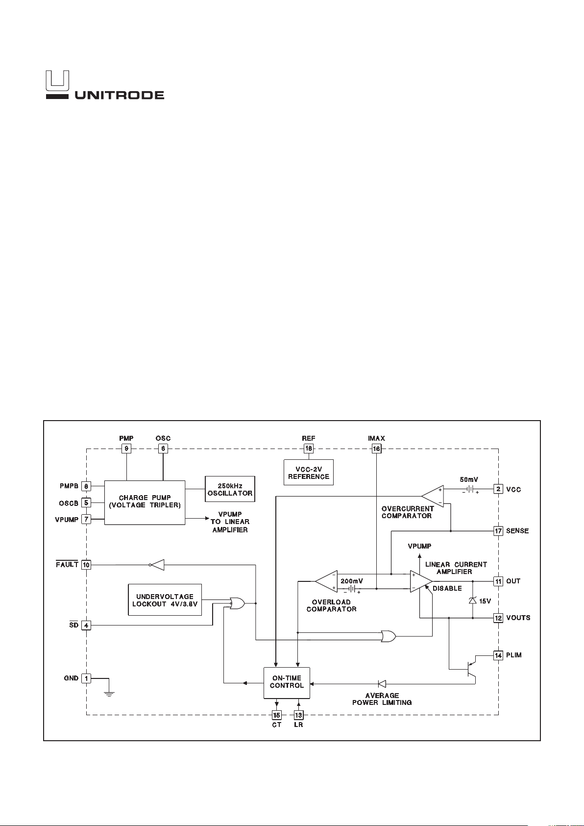
5V to 35V Hot Swap Power Manager
BLOCK DIAGRAM
UDG-95134-2
DESCRIPTION
The UC3914 family of Hot Swap Power Managers provides complete
power management, hot swap and fault handling capability. Integrating this
part and a few external components, allows a board to be swapped in or
out upon failure or system modification without removing power to the hard
-
ware, while maintaining the integrity of the powered system. Complemen
tary output drivers and diodes have been integrated for use with external
capacitors as a charge pump to ensure sufficient gate drive to the external
NMOS transistor for low R
DS(on)
. All control and housekeeping functions
are integrated and externally programmable and include the fault current
level, maximum output sourcing current, maximum fault time and average
power limiting of the external FET. The UC3914 features a duty ratio cur
rent limiting technique, which provides peak load capability while limiting
the average power dissipation of the external pass transistor during fault
conditions. The fault level is fixed at 50mV with respect to VCC to minimize
total dropout. The fault current level is set with an external current sense re
sistor. The maximum allowable sourcing current is programmed by using a
resistor divider from VCC to REF to set the voltage on IMAX. The maximum
current level, when the output appears as a current source is
(VCC – V
IMAX
)/R
SENSE
.
(continued)
2
UC1914
UC2914
UC3914
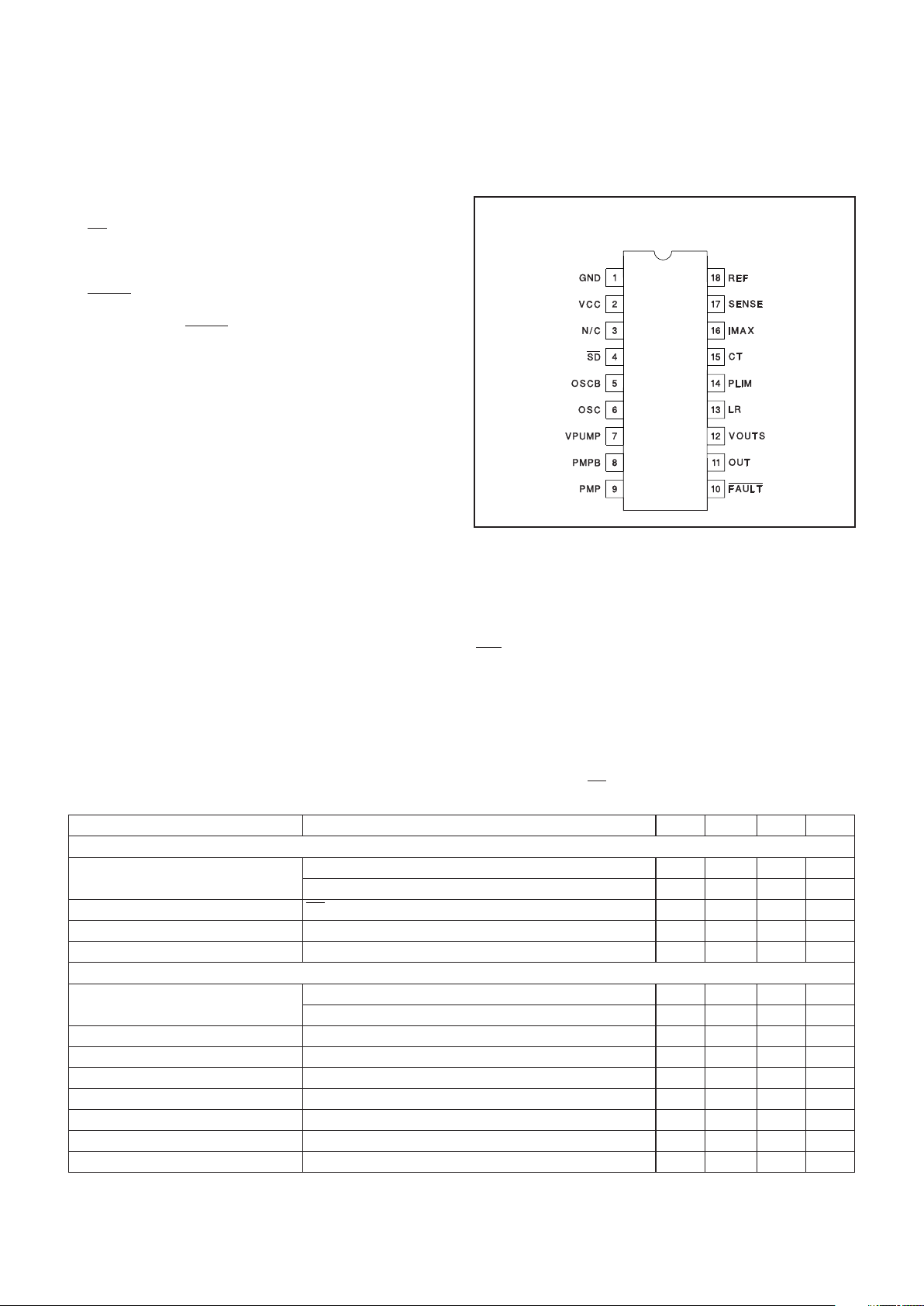
CONNECTION DIAGRAM
ELECTRICAL CHARACTERISTICS:
Unless otherwise specified, TA= 0°C to 70°C for the UC3914, –40°C to 85°C for
the UC2914, and –55°C to 125°C for the UC1914. VCC = 12V, V
PUMP=VPUMP
(max), SD = 5V, CP1 = CP2 = C
PUMP
= 0.01µF.
T
A=TJ
.
PARAMETER TEST CONDITIONS MIN TYP MAX UNITS
VCC Section
I
CC
(Note 2) 8 15 mA
VCC = 35V, (Note 2) 12 20 mA
Shutdown I
CC
SD = 0V 500 900 µA
UVLO Turn on threshold 4.0 4.4 V
UVLO Hysteresis 100 200 350 mV
Fault Timing Section
Overcurrent Threshold T
J
= 25°C, with respect to VCC –55 –50 –45 mV
Over operating temperature, with respect to VCC –57 –50 –42 mV
IMAX Input Bias 13µA
CT Charge Current CT = 1V –140 –100 –60 µA
CT Discharge Current CT = 1V 2.0 3.0 4.5 µA
CT Charge Current CT = 1V, Overload condition –6.0 –3.0 –1.5 mA
CT Fault Threshold 2.25 2.50 2.75 V
CT Reset Threshold 0.45 0.50 0.55 V
Output Duty Cycle Fault condition, I
PL
= 0 1.5 3.0 4.5 %
Input Supply Voltage, VCC . . . . . . . . . . . . . . . . . . . . . . . . . 40V
Maximum Forced Voltage
SD
. . . . . . . . . . . . . . . . . . . . . . . . . . . . . . . . . . . . . . . . . . 12V
IMAX . . . . . . . . . . . . . . . . . . . . . . . . . . . . . . . . . . . . . . . VCC
LR . . . . . . . . . . . . . . . . . . . . . . . . . . . . . . . . . . . . . . . . . . 12V
Maximum Current
FAULT
. . . . . . . . . . . . . . . . . . . . . . . . . . . . . . . . . . . . . 20mA
PLIM . . . . . . . . . . . . . . . . . . . . . . . . . . . . . . . . . . . . . . 10mA
Maximum Voltage, FAULT
. . . . . . . . . . . . . . . . . . . . . . . . . 40V
Reference Output Current . . . . . . . . . . . . . . . Internally Limited
Storage Temperature . . . . . . . . . . . . . . . . . . . –65°C to +150°C
Junction Temperature. . . . . . . . . . . . . . . . . . . –55°C to +150°C
Lead Temperature (Soldering, 10 sec.) . . . . . . . . . . . . . +300°C
Unless otherwise indicated, voltages are referenced to ground.
Currents are positive into, negative out of specified terminal.
Consult Packaging Section of Databook for thermal limitations
and considerations of package.
ABSOLUTE MAXIMUM RATINGS
When the output current is less than the fault level, the
external output transistor remains switched on. When the
output current exceeds the fault level, but is less than the
maximum sourcing level programmed by IMAX, the output remains switched on, and the fault timer starts to
charge C
T
, a timing capacitor. Once CTcharges to 2.5V,
the output device is turned off and C
T
is slowly dis-
charged. Once C
T
is discharged to 0.5V, the IC performs
a retry and the output transistor is switched on again.
The UC3914 offers two distinct reset modes. In one
mode with LR left floating or held low, the IC will repeatedly try to reset itself if a fault occurs as described
above. In the second mode with LR held high, once a
fault occurs, the output is latched off until either LR is
toggled low, the part is shutdown then re-enabled using
SD,
or the power to the part is turned off and then on
again.
This part is offered in both 18 pin DW Wide-Body (SOIC)
and Dual-In-Line (DIL) packages.
DESCRIPTION (cont.)
DIL-18, SOIC-18 (Top View)
N or J Package, DW Package
3
UC1914
UC2914
UC3914
ELECTRICAL CHARACTERISTICS:
Unless otherwise specified, TA= 0°C to 70°C for the UC3914, –40°C to 85°C for the
UC2914, and –55°C to 125°C for the UC1914. VCC = 12V, V
PUMP=VPUMP
(max), SD = 5V, CP1 = CP2 = C
PUMP
= 0.01µF.
T
A=TJ
.
PARAMETER TEST CONDITIONS MIN TYP MAX UNITS
Output Section
OUT High Voltage VOUTS = VCC, VPUMP = VPUMP max, with respect to
VPUMP
–1.5 –1.0 V
OUT High Voltage VOUTS = VCC, VPUMP = VPUMP max, IOUT = –2mA,
with respect to VPUMP
–2.0 –1.5 V
OUT Low Voltage I
OUT
= 0 0.8 1.3 V
I
OUT
= 5mA 1 2 V
I
OUT
= 25mA, Overload Condition, VOUTS = 0V 1.2 1.8 V
OUT Clamp Voltage VOUTS = 0V 11.5 13.0 14.5 V
Rise Time C
OUT
= 1nF (Note 1) 750 1250 ns
Fall Time C
OUT
= 1nF (Note 1) 250 500 ns
Charge Pump Section
OSC, OSCB Frequency 60 150 250 kHz
OSC, OSCB Output High I
OSC
= –5mA 10.0 11.0 11.6 V
OSC, OSCB Output Low I
OSC
= 5mA 0.2 0.5 V
OSC, OSCB Output Clamp Voltage VCC = 25 18.5 20.5 22.5 V
OSC, OSCB Output Current Limit High Side Only –20 –10 –3 mA
Pump Diode Voltage Drop I
DIODE
= 10mA, Measured from PMP to PMPB, PMPB to
VPUMP
0.5 0.9 1.3 V
PMP Clamp Voltage VCC = 25 18.5 20.5 22.5 V
VPUMP Maximum Voltage VCC = 12, VOUTS = VCC, Voltage Where Charge Pump
Disabled
20 22 24 V
VCC = 35V, VOUTS = VCC, Voltage Where Charge
Pump Disabled
42 45 48 V
VPUMP Hysteresis VCC = 12, VOUTS = VCC, Voltage Where Charge Pump
Re-enabled
0.3 0.7 1.4 V
VCC = 35V, VOUTS = VCC, Charge Pump Re-enabled 0.25 0.7 1.4 V
Linear Current Section
Input Offset Voltage –15 0 15 mV
Voltage Gain 60 80 dB
IMAX Control Voltage IMAX = OUT, SENSE = VCC, with respect to VCC –20 0 20 mV
IMAX = OUT, SENSE = REF, with respect to REF –20 0 20 mV
SENSE Input Bias 1.5 3.5 µA
Reference Section
REF Output Voltage With respect to VCC –2.25 –2.00 –1.75 V
REF Current Limit 12.5 20.0 50.0 mA
Load Regulation I
VREF
= 1mA to 5mA 25 60 mV
Line Regulation VCC = 5V to 35V 25 100 mV
Shutdown Section
Shutdown Threshold 0.6 1.5 2.0 V
Input Current SD
= 5V 150 300 µA
Delay to Output (Note 1) 0.5 2.0 µs
Fault Section
Fault Output Low I
FAULT
= 1mA 100 200 mV
Fault Output Leakage V
FAULT
= 35V 10 500 nA
4
UC1914
UC2914
UC3914
PIN DESCRIPTIONS
CT: A capacitor is connected to this pin in order to set
the maximum fault time. The minimum fault time must be
more than the time to charge external load capacitance.
The fault time is defined as:
T
CT
I
FAULT
CH
=
•2
where I
CH
= 100µA+IPL, where IPLis the current into the
power limit pin. Once the fault time is reached the output
will shutdown for a time given by:
T
CT
I
SD
DIS
=
•2
where I
DIS
is nominally 3µA.
FAULT:
Open collector output which pulls low upon any
of the following conditions: Timer fault, Shutdown, UVLO.
This pin MUST be pulled up to VCC or another supply
through a suitable impedance.
GND: Ground reference for the IC.
IMAX: This pin programs the maximum allowable
sourcing current. Since REF is a –2V reference (with re
spect to VCC), a voltage divider can be derived from
VCC to REF in order to generate the program level for
the IMAX pin. The current level at which the output ap
pears as a current source is equal to the voltage on the
IMAX pin, with respect to VCC, divided by the current
sense resistor. If desired, a controlled current startup can
be programmed with a capacitor on IMAX to VCC.
LR: If this pin is held high and a fault occurs, the timer
will be prevented from resetting the fault latch when CT is
discharged below the reset comparator threshold. The
part will not retry until this pin is brought to a logic low or
a power-on-reset occurs. Pulling this pin low before the
reset time is reached will not clear the fault until the reset
time is reached. Floating or holding this pin low will result
in the part repeatedly trying to reset itself if a fault occurs.
OUT: Output drive to the MOSFET pass element. Internal clamping ensures that the maximum V
GS drive is
15V.
OSC, OSCB: Complementary output drivers for intermediate charge pump stages. A 0.01µF capacitor should be
placed between OSC and PMP, and OSCB and PMPB.
PLIM: This feature ensures that the average MOSFET
power dissipation is controlled. A resistor is connected
from this pin to VCC. Current will flow into PLIM which
adds to the fault timer charge current, reducing the duty
cycle from the typical 3% level. When I
PL >> 100µA then
the average MOSFET power dissipation is given by:
P
FET_AVG = IMAX • 3 • 10
–6
•RPL.
PMP, PMPB: Complementary pins which couple charge
pump capacitors to internal diodes and are used to pro
-
vide charge to the reservoir capacitor tied to VPUMP.
Typical capacitor values used are 0.01µF.
REF: –2V reference with respect to VCC used to pro
-
gram the IMAX pin voltage. A 0.1µF ceramic or tantalum
capacitor MUST be tied between this pin and VCC to en
-
sure proper operation of the chip.
SD:
When this TTL compatible input is brought to a logic
low, the output of the linear amplifier is driven low,
FAULT
is pulled low and the IC is put into a low power
mode. The ABSOLUTE maximum voltage that can be
placed on this pin is 12V.
ELECTRICAL CHARACTERISTICS: Unless otherwise specified, T
A
= 0°C to 70°C for the UC3914, –40°C to 85°C for the
UC2914, and –55°C to 125°C for the UC1914. VCC = 12V, V
PUMP=VPUMP
(max), SD = 5V, CP1 = CP2 = C
PUMP
= 0.01µF.
T
A=TJ
.
PARAMETER TEST CONDITIONS MIN TYP MAX UNITS
Latch Section
LR Threshold High to Low 0.6 1.4 2.0 V
Input Current LR = 5V 500 750 µA
Power Limiting Section
Duty Cycle Control In Fault, I
PLIM
= 200µA 0.6 1.3 2.0 %
In Fault, I
PLIM
= 3mA 0.05 0.12 0.20 %
Overload Section
Delay to Output (Note 1) 500 1250 ns
Threshold Respect to IMAX –250 –200 –150 mV
Note 1: Guaranteed by design. Not 100% tested in production.
Note 2: A mathematical averaging is used to determine this value. See Application Section for more information.
5
UC1914
UC2914
UC3914
SENSE: Input voltage from current sense resistor. When
there is greater than 50mV across this pin with respect to
VCC, a fault is sensed and C
T
begins to charge.
VCC: Input voltage to the IC. Typical voltages are 4.5V to
35V. The minimum input voltage required for operation is
4.5V.
VOUTS: Source connection of external N-channel MOS
-
FET and sensed output voltage of load.
VPUMP: Charge pump output voltage. A capacitor
should be tied between this pin and VOUTS with a typi
-
cal value being 0.01µF.
PIN DESCRIPTIONS (cont.)
0
0.5
1
1.5
2
2.5
3
3.5
-55 -40 0 25 70 85 125
TEMPERATURE (°C)
V
IO
(mV)
Linear Amp VIOvs. Temperature
-52
-51.5
-51
-50.5
-50
-49.5
-49
-48.5
-48
-55 -40 0 25 70 85 125
TEMPERATURE (°C)
FAULT THRESHOLD (mV)
Fault Threshold vs. Temperature
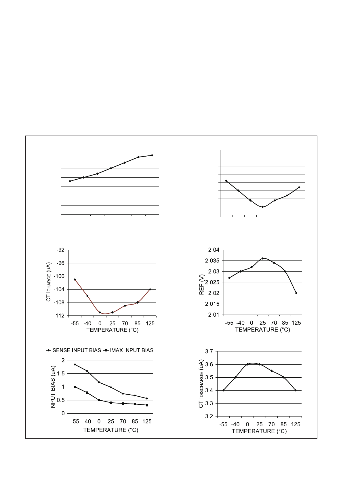
CT I
CHARGE
vs. Temperature VCC - REF vs Temperature
I
MAX
& SENSE Input Bias vs. Temperature
CT I
DISCHARGE
vs. Temperature
Figure 1. Typical characteristic curves.
TYPICAL CHARACTERISTIC CURVES

6
UC1914
UC2914
UC3914
Figure 2. Fault timing circuitry for the UC3914, including power limit and overcurrent.
UDG-97052
The UC3914 is to be used in conjunction with external
passive components and an N-channel MOSFET
(NMOS) to facilitate hot swap capability of application
modules. A typical application set-up is given in Fig. 9.
The term hot swap refers to the system requirement that
submodules be swapped in or out upon failure or system
modification without removing power to the operating
hardware. The integrity of the power bus must not be
compromised due to the addition of an unpowered mod
ule. Significant power bus glitches can occur due to the
substantial initial charging current of on-board module
bypass capacitance and other load conditions (for more
information on hot swapping and power management ap
plications, see Application Note U-151). The UC3914
provides protection by monitoring and controlling the out
put current of an external NMOS to charge this capaci
tance and provide load current. The addition of the
NMOS, a sense resistor, R
SENSE,
and two other resis
tors, R1 and R2, sets the programmed maximum current
level the NMOS can source to charge the load in a controlled manner. The equation for this current, I
MAX
, is:
I
VV
R
MAX
CC IMAX
SENSE
=
−
where V
IMAX
is the voltage generated at the IMAX pin.
Analysis of the application circuit shows that V
IMAX
(with
respect to GND) can be defined as:
()
VV
VV R
RR
VR
RR
V
IMAX REF
CC REF
REF
=+
−•
+
=
•
+
+
1
12
21
12
where V
REF
is the voltage on the REF pin and whose in
ternally generated potential is two volts below VCC. The
UC3914 also has an internal overcurrent comparator
which monitors the voltage between SENSE and VCC. If
this voltage exceeds 50mV, the comparator determines
that a fault has occurred, and a timing capacitor, C
T,
will
begin to charge. This can be rewritten as a current which
causes a fault, I
FAULT
:
I
mV
R
FAULT
SENSE
=
50
Fault Timing
Fig. 2 shows the circuitry associated with the fault timing
function of the UC3914. A typical fault mode, where the
overload comparator and current source I3 do not factor
into operation (switch S2 is open), will first be considered. Once the voltage across R
SENSE
exceeds 50mV, a
fault has occurred. This causes the timing capacitor, C
T
,
to charge with a combination of 100µA (I1) plus the current from the power limiting circuitry (I
PL
).
APPLICATION INFORMATION

7
UC1914
UC2914
UC3914
Figure 3a: Typical timing diagram.
UDG-97054
t0: Normal conditions - output current is nominal, output
voltage is at positive rail, VCC
t1: Fault control reached - output current rises above the
programmed fault value, C
T
begins to charge with ≅
100µA + I
PL
.
t2: Maximum current reached - output current reaches
the programmed maximum level and becomes a con
-
stant current with value IMAX.
t3: Fault occurs - C
T
has charged to 2.5V, fault output
goes low, the FET turns off allowing no output current
to flow, VOUT discharge to GND.
t4: Retry - C
T
has discharged to 0.5V, but fault current
is still exceeded, C
T
begins charging again, FET is on,
VOUT increases.
t5 = t3: Illustrates <3% duty cycle depending upon
R
PL
selected.
t6 = t4
t7 = t0: Fault released, normal condition - return to
normal operation of the hot swap power manager.
Fig. 3a shows typical fault timing waveforms for the ex
ternal NMOS output current, the voltage on the CT pin,
and the output load voltage, V
OUT
, with LR left floating or
grounded. The output voltage waveforms have assumed
an RC characteristic load and time constants will vary de
-
pending upon the component values. Prior to time t
0, the
load is fully charged to almost VCC and the NMOS is
supplying the current, I
O
, to the load. At t0, the current
begins to ramp up due to a change in the load conditions
until, at t
1, the fault current level, I
FAULT,
has been
reached to cause switch S1 to close. This results in C
T
being charged with the current sources I1 and IPL. Dur
-
ing this time, V
OUT
is still almost equal to VCC except for
small losses from voltage drops across the sense resis
-
tor and the NMOS. The output current reaches the pro
-
grammed maximum level, I
MAX,
at t2. The CTvoltage
continues to rise since I
MAX
is still greater than I
FAULT
.
The load output voltage drops because the current load
requirements have become greater than the controlled
maximum sourcing current. The C
T
voltage reaches the
upper comparator threshold (Fig. 2) of 2.5V at t
3, which
promptly shuts off the gate drive to the NMOS (not
APPLICATION INFORMATION (cont.)

8
UC1914
UC2914
UC3914
shown but can be inferred from the fact that no output
current is provided to the load), latches in the fault and
opens switch S1 disconnecting the charging currents I1
and I
PL
from CT. Since no output current is supplied, the
load voltage decays at a rate determined by the load
characteristics and the capacitance. The 3µA current
source, I2, discharges CT to the 0.5V reset comparator
threshold. This time is significantly longer than the charg
ing time and is the basis for the duty cycle current limiting
technique. When the C
T
voltage reaches 0.5V at t4, the
part performs a retry, allowing the NMOS to again source
current to the load and cause V
OUT to rise. In this partic
-
ular example, I
MAX
is still sourced by the NMOS at each
attempted retry and the fault timing sequence is repeated
until time t7 when the load requirements change to I
O.
Since IOis less than the fault current level at this time,
switch S1 is opened, I2 discharges C
T
and V
OUT
rises to
almost VCC.
Fig. 3b shows fault timing waveforms similar to those depicted in Fig. 3a except that the latch reset (LR) function
is utilized. Operation is the same as described above until t4 when the voltage on C
T
reaches the reset threshold.
Holding LR high prevents the latch from being reset, preventing the IC from performing a retry (sourcing current
to the load). The UC3914 is latched off until either LR is
pulled to a logic low, or the chip is forced into an under
voltage lockout (UVLO) condition and back out of UVLO
causing the latch to automatically perform a power on reset. Fig. 3b illustrates LR being toggled low at t5, causing
the part to perform a retry. Time t
6 again illustrates what
happens when a fault is detected. The LR pin is toggled
low and back high at time t7, prior to the voltage on the
CT pin hitting the reset threshold. This information tells
the UC3914 to allow the part to perform a retry when the
lower reset threshold is reached, which occurs at t8.
Time t9 corresponds to when load conditions change to
where a fault is not present as described for Fig. 3a.
Power Limiting
The power limiting circuitry is designed to only source
current into the CT pin. To implement this feature, a re
-
sistor, R
PL
, should be placed between VCC and PLIM.
The current, I
PL
(show in Fig. 2) is given by the following
expression:
I
VV
R
for V V V
PL
CC OUTS
PL
OUTS CT
=
−
>+,1
where V
CT
is the voltage on the CT pin. For V
OUTS
<1V
+V
CT
the common mode range of the power limiting cir
-
cuitry causes I
PL
= 0 leaving only the 100µA current
source to charge C
T.VCC–VOUTS
represents the volt
-
age across the NMOS pass device.
Later it will be shown how this feature will limit average
power dissipation in the pass device. Note that under a
fault condition where the output current is just above the
fault level, but less than the maximum level, V
OUTS
~
VCC, I
PL
= 0 and the CTcharging current is 100µA.
During a fault, the CT pin will charge at a rate deter
mined by the internal charging current and the external
timing capacitor, C
T.
Once CTcharges to 2.5V, the fault
comparator trips and sets the fault latch. When this oc
curs, OUT is pulled down to VOUTS, causing the exter
nal NMOS to shut off and the charging switch, S1, to
open. C
T
will be discharged with I2 until the CTpotential
reaches 0.5V. Once this occurs, the fault latch will reset
(unless LR is being held high, whereby a fault can only
be cleared by pulling this pin low or going through a
power-on-reset cycle), which re-enables the output of the
linear amplifier and allows the fault circuitry to regain
control of the charging switch. If a fault is still present,
the overcurrent comparator will close the charging switch
causing the cycle to repeat. Under a constant fault the
duty cycle is given by:
Duty Cycle
A
IA
PL
=
+3100µµ
Average power dissipation can be limited using the PLIM
pin. Average power dissipation in the pass element is
given by:
()
()
PFETavg VCC V I Duty Cycle
VCC V I
OUTS MAX
OUTS MAX
=− ••
=− ••
3 µ
A
IA
PL
+ 100 µ
VCC – VOUTS is the drain to source voltage across the
FET. When IPL >> 100µA, the duty cycle equation given
above can be rewritten as:
()
Duty Cycle
RPL A
VCC VOUTS
=
•−3µ
and the average power dissipation of the MOSFET is
given by:
()
()
PFETavg
VCC VOUTS IMAX
RPL A
VCC VOUTS
IMAX RPL
=− ••
•
−
=••
33µ
µ
A
The average power is limited by the programmed IMAX
current and the appropriate value for R
PL
.
APPLICATION INFORMATION (cont.)

9
UC1914
UC2914
UC3914
Figure 3b. Typical timing diagram utilizing LR (Latch Reset) function.
APPLICATION INFORMATION (cont.)
t0: Normal conditions - output current is nominal, output
voltage is at positive rail, VCC
t1: Fault control reached - output current rises above the
programmed fault value, C
T begins to charge with ≅
100µA + I
PL.
t2: Maximum current reached - output current reaches
the programmed maximum level and becomes a con
-
stant current with value IMAX.
t3: Fault occurs - C
T has charged to 2.5V, fault output
goes low, the FET turns off allowing no output current to
flow, VOUT discharge to GND.
t4: Reset comparator threshold reached but no retry
since LR pin held high.
t5: LR toggled low, NMOS turned on and sources cur
-
rent to load.
t6 = t3
t7: LR toggled low before V
CT reaches reset compara
-
tor threshold, causing retry.
t8: Since LR toggled low during present cycle, NMOS
turned on and sources current to load.
t9 = t0: Fault released, normal condition - return to
normal operation of the hot swap power manager.
UDG-97055

10
UC1914
UC2914
UC3914
Overload Comparator
The linear amplifier in the UC3914 ensures that the ex
ternal NMOS does not source more than the current
I
MAX, defined above as:
I
VCC V
R
MAX
IMAX
SENSE
=
−
In the event that output current exceeds the programmed
I
MAX
by more than 200mV/R
SENSE,
the output of the lin
ear amplifier will immediately be pulled low (with respect
to VOUTS) providing no gate drive to the NMOS, and
preventing current from being delivered to the load. This
situation could occur if the external NMOS is not re
sponding to a command from the IC or output load condi
tions change quickly to cause an overload condition
before the linear amplifier can respond. For example, if
the NMOS is sourcing current into a load and the load
suddenly becomes short circuited, an overload condition
may occur. The short circuit will cause the V
GS
of the
NMOS to immediately increase, resulting in increased
load current and voltage drop across R
SENSE.
If this drop
exceeds the overload comparator threshold, the amplifier
output will be quickly pulled low. It will also cause the CT
pin to begin charging with I3, a 3mA current source (refer
to Fig. 2) and continue to charge until approximately one
volt below VCC, where it is clamped. This allows a constant fault to show up on FAULT
and since the voltage on
CT will only charge past 2.5V in an overload fault condition, it can be used for detection of output NMOS failure
or to build redundancy into the system.
Estimating Minimum Timing Capacitance
The startup time of the IC may not exceed the fault time
for the application. Since the timing capacitor, C
T
, deter
-
mines the fault time, its minimum value can be deter
mined by calculating the startup time of the IC. The
startup time is dependent upon several external compo
nents. A load capacitor, C
LOAD
, should be tied between
VOUTS and GND. Its value should be greater than that
of C
PUMP,
the reservoir capacitor tied from V
PUMP
to
V
OUTS
(see Fig. 4). Given values of C
LOAD,
Load,
R
SENSE
, VCC and the resistors determining the voltage
on I
MAX
, the user can calculate the approximate startup
time of the node V
OUT.
This time must be less than the
time it takes for C
T
to charge to 2.5V. Assuming the user
has determined the fault current, R
SENSE
can be calcu
-
lated by:
R
mV
I
SENSE
FAULT
=
50
I
MAX
is the maximum current the UC3914 will allow
through the transistor M1. During startup with an output
capacitor, M1 can be modeled as a constant current
source of value I
MAX
where:
I
VCC V
R
MAX
IMAX
SENSE
=
−
Given this information, calculation of startup time is now
possible via the following:
Current Source Load:
T
CVCC
II
START
LOAD
MAX LOAD
=
•
–
Resistive Load:
TRCn
VCC
IR
START LOAD LOAD
MAX LOAD
=− • • −
•
l 1
The only remaining external component which may af
fect the minimum timing capacitor is the optional power
limiting resistor, R
PL
. If the addition of RPLis desirable,
its value can be determined from the “Fault Timing” section above. The minimum timing capacitor values are
now given by
Current Source Load:
CT T
R
VCC
R
START
PL
PL
min =•
•+
•
−
10
2
2
4
APPLICATION INFORMATION (cont.)
Figure 4. Estimating minimum timing capacitor.
UDG-97056

11
UC1914
UC2914
Resistive Load:
()
()
CT
RV I R T
R
V
R
PL CC MAX LOAD START
PL
CC
PL
min =
•+− • •
•
+•
−
10
2
2
4
RC
LOAD LOAD
•
Output Current Softstart
The external MOSFET output current can be increased
at a user-defined rate to ensure that the output voltage
comes up in a controlled fashion by adding capacitor
C
SS
, as shown in Fig. 5. The chip does place one con
straint on the soft start time and that is that the charge
pump time constant has to be much less than the
softstart time constant to ensure proper soft start opera
tion. The time constant determining the startup time of
the charge pump is given by:
τ
CP OUT PUMP
RC
=•
R
OUT
is the output impedance of the charge pump given
by:
R
fCP
OUT
PUMP
=
•
1
where f
PUMP
is the charge pump frequency (125kHz) and
CP = CP1 = CP2 are the charge pump flying capacitors.
For typical values of CP1, CP2 and C
PUMP
(0.01µF) and
a switching frequency of 125kHz, the output impedance
is 800Ω and the charge pump time constant is 8µs. The
charge pump should be close to being fully charged in 3
time constants or 24µs. By placing a capacitor from VCC
to IMAX, the voltage at IMAX, which sets the maximum
output current of the FET, will exponentially decay from
VCC to the desired value set by R1 and R2. The output
current of the MOSFET will be controlled via soft start as
long as the soft start time constant (τ
SS
) is much greater
than the charge pump time constant τ
CP
, given by
()
τ
SS SS
RR C
=•12
Minimizing Total Dropout Under Low Voltage
Operation
In a typical application, the UC3914 will be used to con
trol the output current of an external NMOS during hot
swapping situations. Once the load has been fully
charged, the desired output voltage on the load, V
OUT
,
will be required to be as close to VCC as possible to
minimize total dropout. For a resistive load, R
LOAD,
the
output voltage is given by:
V
R
RR R
VCC
OUT
LOAD
LOAD SENSE DS on
=
++
•
()
R
SENSE
was picked to set the fault current, I
FAULT
.
R
DS(on)
, the on-resistance of the NMOS, should be made
as small as possible to ensure V
OUT
is as close to VCC
as possible. For a given NMOS, the manufacturer will
specify the R
DS(on)
for a certain VGS(maybe 7V to 10V).
The source potential of the NMOS is V
OUT.
In order to
ensure sufficient VGS, this requires the gate of the
NMOS, which is the output of the linear amplifier, to be
many volts higher than VCC. The UC3914 provides the
capability to generate this voltage through the addition of
3 capacitors, CP1, CP2 and C
PUMP
as shown in Fig. 6.
These capacitors should be used in conjunction with the
complementary output drivers and internal diodes in
cluded on-chip to create a charge pump or voltage
tripler. The circuit boosts VCC by utilizing capacitors
CP1, CP2 and C
PUMP
in such a way that the voltage at
V
PUMP
approximately equals (3 • VCC)–(5•V
DIODE
), al
most tripling the input supply voltage to the chip.
APPLICATION INFORMATION (cont.)
6 11
129
8
7
C
PUMP
L
O
A
D
C
LOAD
V
OUT
M1
2
OUT
VOUTS
VPUMP
VCC
R2
18 16
C
SS
R1
C1
IMAXREF
OSC
PMP
5
OSCB
PMPB
CP2
CP1
Figure 5. MOSFET soft start diagram.
UDG-98160
Figure 6. Charge pump block diagram.
UDG-97058

12
UC1914
On each complete cycle, CP1 is charged to approxi
-
mately V
CC
–V
DIODE
(unless VCCis greater than 15V
causing internal clamping to limit this charging voltage to
about 13V) when the output Q of the toggle flip flop is
low. When Q
is transitioned low (and Q correspondingly
is brought high), the negative side of CP2 is pulled to
ground, and CP1 charges CP2 up to about (2 • V
CC
–3•
V
DIODE
). When Q is toggled high, the negative side of
CP2 is brought to (V
CC–VDIODE
). Since the voltage
across a capacitor cannot change instantaneously with
time, the positive side of the capacitor swings up to (3 •
V
CC
–4•V
DIODE
). This charges C
PUMP
up to (3 • VCC–
5 • V
DIODE
).
The maximum output voltage of the linear amplifier is ac
tually less than this because of the ability of the amplifier
to swing to within approximately 1V of V
PUMP
. Due to in
efficiencies of the charge pump, the UC3914 may not
have sufficient gate drive to fully enhance a standard
power MOSFET when operating at input voltages below
7V. Logic Level MOSFETs could be used depending on
the application but are limited by their lower current capability. For applications requiring operation below 7V there
are two ways to increase the charge pump output voltage. Fig. 7 shows the typical tripler of Fig. 6 enhanced
with three external schottky diodes. Placing the schottky
diodes in parallel with the internal charge pump diodes
decreases the voltage drop across each diode thereby
increasing the overall efficiency and output voltage of the
charge pump.
Fig. 8 shows a way to use the existing drivers with exter
nal diodes (or Schottky diodes for even higher pump
voltages but with additional cost) and capacitors to make
a voltage quadrupler. The additional charge pump stage
will provide a sufficient pump voltage (V
PUMP
=4•VCC–
7•V
DIODE
) to generate the maximum VGS. Operation is
similar to the case described above. This additional cir
cuitry is not necessary for higher input voltages because
the UC3914 has internal clamping which only allows
V
PUMP
to be 10V greater than V
OUTS
.
Input
Voltage
(VCC)
Internal
Diodes
(V
GS
)
External
Schottky
Diodes (VGS)
Quadrupler
(VGS)
4.5 4.57 6.8 8.7
5 5.8 7.9 8.8
5.5 6.6 8.6 8.9
6 7.6 8.8 9
6.5 8.7 8.8 9
7 8.8 9 9
9 9.2 9.4 9.1
10 9.3 9.4 9.3
Table 1. UC3914 charge pump characteristics.
Table 1 characterizes the UC3914 charge pump in its
standard configuration, with external schottky diodes,
and configured as a voltage quadrupler. Please note:
The voltage quadrupler is unnecessary for input voltages
above 7.0V due the internal clamping action.
ICC Specification
The ICC operating measurement is actually a mathe
-
matical calculation. The charge pump voltage is con
-
stantly being monitored with respect to both V
CC
and
V
OUTS
to determine whether the pump requires servic
ing. If there is insufficient voltage on this pin, the charge
pump drivers are alternately switched to raise the volt
age of the pump (see Fig. 9). Once the voltage on the
pump is high enough, the drivers and other charge pump
related circuitry are shutdown to conserve current. The
pump voltage will decay due to internal loading until it
reaches a low enough level to turn the drivers back on.
The chip requires significantly different amounts of cur
rent during these two modes of operation and the follow
ing mathematical calculation is used to figure out the
average current:
ICC
ICC T ICC T
TT
DRIVERS on ON DRIVERS off OFF
ON OF
=
•+ •
+
() ( )
F
APPLICATION INFORMATION (cont.)
8
7
5
6
CP2
Q
Q
250kHz
OSCILLATOR
TOGGLE
FLIP FLOP
9 2
D1
D2
D3
C
PUMP
TO VOUT
VPUMP
OSCB
CP1
OSC
T
VCCPMP
PMPB
Figure 7. Enhanced charge pump block diagram.
UDG-98204

13
UC1914
UC2914
UC3914
PUMP
PUMP UPPER LEVEL
PUMP LOWER LEVEL
"PUMP"
SERVICING FREQUENCY
OSCILLATOR FREQUENCY
T
ON
T
OFF
OSC
OSCB
TIME
Figure 9. Charge pump waveforms.
UDG-98144
Since the charge pump does not always require servic
ing, the user may think that the charge pump frequency
is much less than the datasheet specification. This is not
the case as the free-running frequency is guaranteed to
be within the datasheet limits. The charge pump servic
ing frequency can make it appear as though the drivers
are operating at a much lower frequency.
APPLICATION INFORMATION (cont.)
Figure 8. Low voltage operation to produce higher
pump voltage.
UDG-97059

14
UC1914
UC2914
UC3914
UNITRODE CORPORATION
7 CONTINENTAL BLVD. • MERRIMACK, NH 03054
TEL. (603) 424-2410 FAX (603) 424-3460
14
12
11
17
2
10
4
5
9 18
1
8
7
166
1513
15V
+
–
VPUMP
PLIM
VOUTS
OUT
+
–
+
–
++
+
–
1.4V
+
–
+
–
2.5V
0.5V
SQ
QR
FAULT
TIMING
CIRCUITRY
FAULT
LATCH
3m
A
H=CLOSE
3mA 103mA
UNDERVOLTAGE
LOCKOUT
4.0V / 3.8V
TO LINEAR
AMPLIFIER
VOUT +10V
(45V
MAX
)
VCC – 2V
REFERENCE
250kHz
OSCILLATOR
T
TOGGLE
VCC
+
–
C
T
CTLR
GND
R
FAULT
TO VCC
C
PUMP
TO V
OUT
VPUMP
CP2
PMPB
OSCB
CP1
PMP OSC
R1 R2
C1
C2
SENSE
R
SENSE
VCC
V
OUT
R
PL
VCC
LINEAR
AMPLIFIER
FAULT=
50mV
H=CLOSE
OVERCURRENT
COMPARATOR
OVERLOAD
COMPARATOR
200mV
50mV
IMAXREF
SD
FAULT
Figure 10. Typical application.
APPLICATION INFORMATION (cont.)
UDG-98194
SAFETY RECOMMENDATIONS
Although the UC3914 is designed to provide system pro
tection for all fault conditions, all integrated circuits can
ultimately fail short. For this reason, if the UC3914 is in
tended for use in safety critical applications where UL or
some other safety rating is required, a redundant safety
device such as a fuse should be placed in series with
the device. The UC3914 will prevent the fuse from blow
-
ing in virtually all fault conditions, increasing system reli
ability and reducing maintainence cost, in addition to
providing the hot swap benefits of the device.
 Loading...