

Datasheet UC3854DW, UC3854QTR, UC3854Q, UC3854N, UC3854DWTR Datasheet (Texas Instruments)
...
6/98
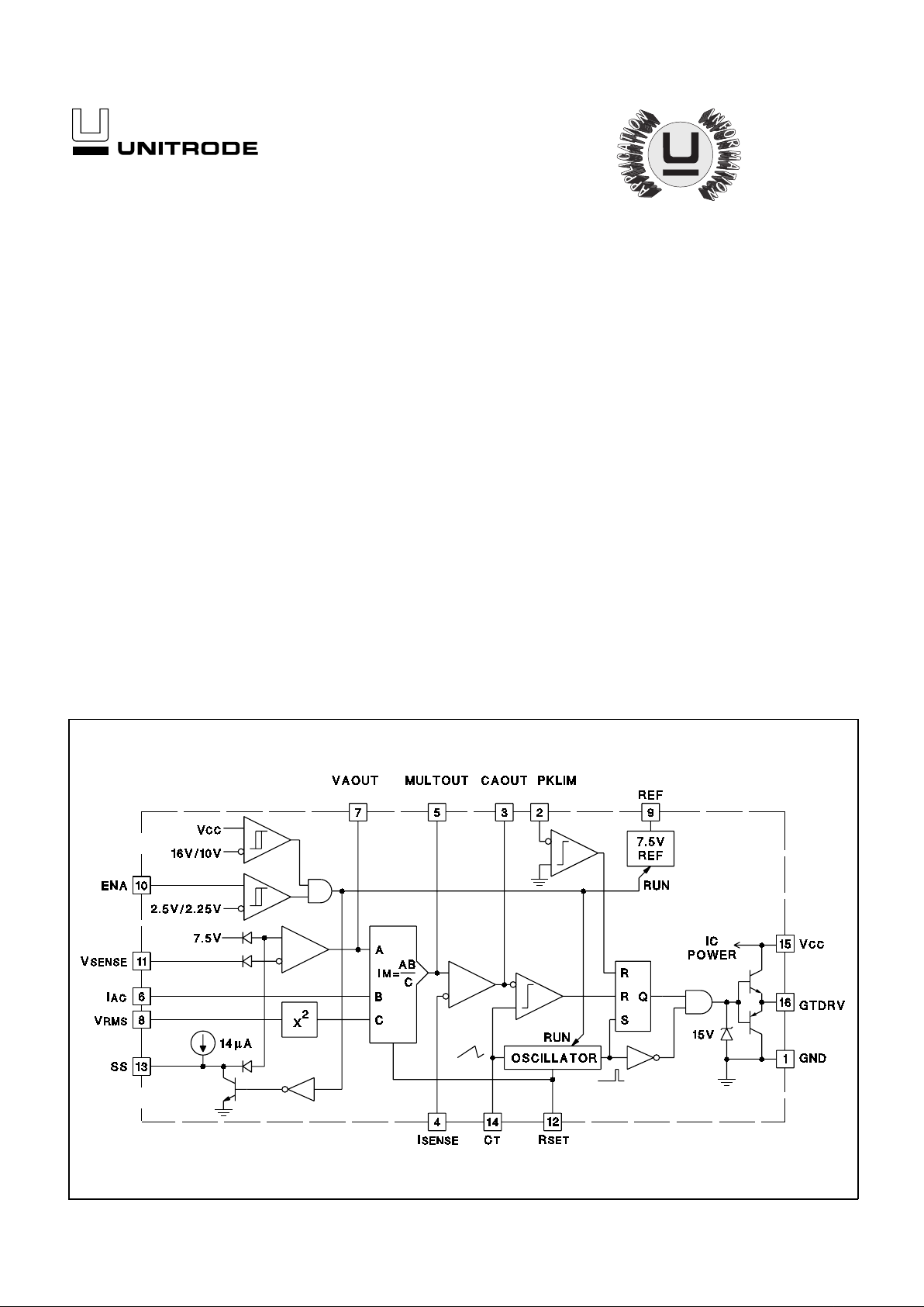
BLOCK DIAGRAM
• Control Boost PWM to 0.99 Power Factor
• Limit Line Current Distortion To <5%
• World-Wide Operation Without Switches
• Feed-Forward Line Regulation
• Average Current-Mode Control
• Low Noise Sensitivity
• Low Start-Up Supply Current
• Fixed-Frequency PWM Drive
• Low-Offset Analog Multiplier/Divider
• 1A Totem-Pole Gate Driver
• Precision Voltage Reference
The UC1854 provides active power factor correction for power systems t hat otherwise would draw non-sinusoidal current from sinusoidal power lines. This device implements all the control functions
necessary to build a power supply capable of optimally using available
power- line current w hile mini mizing line-cur rent distort ion. To do t his,
the UC1854 contains a vo ltage amplifier, an analog m ultiplier/divider,
a current amplifier, and a fixed-frequency PWM. In addition, the
UC1854 c ontains a power MOSFET compatible gat e driver, 7.5V refere nce, line anticipator, load-enable comparator, low-su pply detector,
and over-current comparator.
The UC1854 us es average current-mode control to accompli sh fixedfreque ncy current control with stability and low distortion. Unlike peak
current-mode, average current control accurately maintains sinusoidal
line curr ent without slope compensation and with minimal response to
noise transients.
The UC1854’s high reference voltage and high oscillator amplitude
minimi ze noise s ensitivity while fas t PWM elements permit choppi ng
freque ncies above 2 00kHz. The UC1854 can b e used in single and
three pha se systems with line voltages that vary from 75 to 275 volts
and l ine frequencies acr oss the 50Hz to 400H z range. To reduce the
bur den on t he cir cui try t hat s uppl ies pow er to this device, the UC1854
features low starting supply current.
These devi ces are available pack aged in 16-pin plastic and ceramic
dual in-line packages, and a variety of surface-mount packages.
UC1854
UC2854
UC3854
High Power Factor Preregulator
FEATURES
DESCRIPTION
UDG-92055
Supply Voltage VCC. . . . . . . . . . . . . . . . . . . . . . . . . . . . . . . . . . . . 35V
GT Drv Current, Continuous . . . . . . . . . . . . . . . . . . . . . . . . . . . . 0.5A
GT Drv Current, 50% Duty Cycle. . . . . . . . . . . . . . . . . . . . . . . . . 1.5A
Input Voltage, V
SENSE
, V
RMS
. . . . . . . . . . . . . . . . . . . . . . . . . . . . . 11V
Input Voltage, I
SENSE
, Mult Out . . . . . . . . . . . . . . . . . . . . . . . . . . . 11V
Input Voltage, PKLMT . . . . . . . . . . . . . . . . . . . . . . . . . . . . . . . . . . . 5V
Input Current, R
SET
, IAC, PKLMT, ENA . . . . . . . . . . . . . . . . . . . 10mA
Power Dissipation . . . . . . . . . . . . . . . . . . . . . . . . . . . . . . . . . . . . . 1W
Storage Temperature . . . . . . . . . . . . . . . . . . . . –65
o
C to +150oC
Lead Temperature (Soldering, 10 Seconds) . . . . . . . . . . . . . . +300
o
C
ABSOLUTE MAXIMUM RATINGS
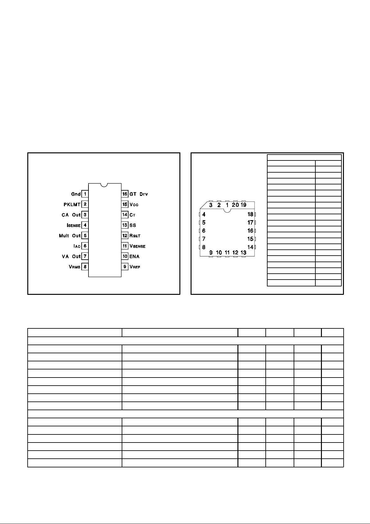
PACK AGE PIN FUN CTION
FUNCTION PIN
N/C 1
Gnd 2
PKLMT 3
CA Out 4
I
SENSE
5
N/C 6
Mult Out 7
I
AC
8
VA Out 9
V
RMS
10
N/C 11
V
REF
12
ENA 13
V
SENSE
14
R
SET
15
N/C 16
SS 17
C
T
18
V
CC
19
GT Drv 20
PLCC-20 & LCC-20
(Top V ie w )
Q & L Packages
CONNECTION DIAGRAMS
DIL–16 & SOIC-16
(Top V ie w )
J, N & DW Packages
Unless otherwise stated, VCC=18V, R
SET
=15k to ground, CT=1.5nF to ground, PKLMT=1V, ENA=7.5V,
V
RMS
=1.5V, IAC=100µA, I
SENSE
=0V, CA Out=3.5V, VA Out=5V, V
SENSE
=7.5V, no load on SS, CA Out,
VA Out, REF, GT Drv, –55
o
C<TA<125oC for the UC1854, –40oC<TA<85oC for the UC2854, and
0
o
C<TA<70oC for the UC3854, and TA=TJ.
ELECTRICAL
CHARACTERISTICS
PARAMETER TEST CONDITIONS MIN TYP MAX UNITS
OVERALL
Supply Current, Off ENA=0V 1.5 2.0 mA
Supply Current, On 10 16 mA
V
CC
Turn-On Threshold 14.5 16 17.5 V
VCC Turn-Off Threshold 9 10 11 V
ENA Threshold, Rising 2.4 2.55 2.7 V
ENA Threshold Hysteresis 0.2 0.25 0.3 V
ENA Input Current ENA=0V –5.0 –0.2 5.0 µA
V
RMS
Input Current V
RMS
=5V –1.0 –.01 1.0 µA
VOLTAGE AMPLIFIER
Voltage Amp Offset Voltage VA Out=5V –8 8 mV
V
SENSE
Bias Current –500 –25 500 nA
Voltage Amp Gain 70 100 dB
Voltage Amp Output Swing 0.5 to 5.8 V
Voltage Amp Short Circuit Current VA Out=0V –36 –20 –5 mA
SS Current SS=2.5V –20 –14 –6 µA
UC1854
UC2854
UC3854
Note 1: All voltages with respect to Gnd (Pin 1).
Note 2: All currents are positive into the specified terminal.
Note 3: ENA input is internally clamped to approximately
14V.
Note 4: Consult Unitrode Integrated Circuits databook for
information regarding thermal specifications and limita-
2
PARAMETER TEST CONDITIONS MIN TYP MAX UNITS
CURRENT AMPLIFIER
Current Amp Offset Voltage –4 4 mV
I
SENSE
Bias Current –500 –120 500 nA
Input Range, I
SENSE
, Mult Out –0.3 to 2.5 V
Current Amp Gain 80 110 dB
Current Amp Output Swing 0.5 to 16 V
Current Amp Short Circuit Current CA Out=0V –36 –20 –5 mA
Current Amp Gain-BW Product T
A
=25oC (Note 6) 400 800 kHz
REFERENCE
Reference Output Voltage I
REF
=0mA, TA=25oC 7.4 7.5 7.6 V
I
REF
=0mA, Over Temp. 7.35 7.5 7.65 V
V
REF
Load Regulation –10mA<I
REF
<0mA –15 5 15 mV
V
REF
Line Regulation 15V<VCC<35V –10 2 10 mV
V
REF
Short Circuit Current REF=0V –50 –28 –12 mA
MULTIPLIER
Mult Out Current I
AC
Limited IAC=100µA, R
SET
=10k, V
RMS
=1.25V –220 –200 –180 µA
Mult Out Current Zero IAC=0µA, R
SET
=15k –2.0 –0.2 2.0 µA
Mult Out Current R
SET
Limited IAC=450µA, R
SET
=15k, V
RMS
=1V, VA Out = 6V –280 –255 –220 µA
Mult Out Current IAC=50µA, V
RMS
=2V, VA=4V –50 –42 –33 µA
IAC=100µA, V
RMS
=2V, VA=2V –38 –27 –12 µA
I
AC
=200µA, V
RMS
=2V, VA=4V –165 –150 –105 µA
IAC=300µA, V
RMS
=1V, VA=2V –250 –225 –150 µA
IAC=100µA, V
RMS
=1V, VA=2V –95 –80 –60 µA
Multiplier Gain Constant (Note 5) –1.0 V
OSCILLATOR
Oscillator Frequency R
SET
=15k 46 55 62 kHz
R
SET
=8.2k 86 102 118 kHz
CT Ramp Peak-to-Valley Amplitude 4.9 5.4 5.9 V
CT Ramp Valley Voltage 0.8 1.1 1.3 V
GATE DRIVER
Maximum GT Drv Output Voltage 0mA load on GT Drv, 18V<V
CC
<35V 13 14.5 18 V
GT Drv Output Voltage High –200mA load on GT Drv, VCC=15V 12 12.8 V
GT Drv Output Voltage Low, Off VCC=0V, 50mA load on GT Drv 0.9 1.5 V
GT Drv Output Voltage Low 200mA load on GT Drv 1.0 2.2 V
10mA load on GT Drv 0.1 0.4 V
Peak GT Drv Current 10nF from GT Drv to Gnd 1.0 A
GT Drv Rise/Fall Time 1nF from GT Drv to Gnd 35 ns
GT Drv Maximum Duty Cycle V
CA Out
=7V 95 %
CURRENT LIMIT
PKLMT Offset Voltage –10 10 mV
PKLMT Input Current PKLMT=–0.1V –200 –100 µA
PKLMT to GT Drv Delay PKLMT falling from 50mV to –50mV 175 ns
Unless otherwise stated, V
CC
=18V, R
SET
=15k to ground, CT=1.5nF to ground, PKLMT=1V, ENA=7.5V,
V
RMS
=1.5V, IAC=100µA, I
SENSE
=0V, CA Out=3.5V, VA Out=5V, V
SENSE
=7.5V, no load on SS, CA Out,
VA Out, REF, GT Drv, –55
o
C<TA<125oC for the UC1854, –40oC<TA<85oC for the UC2854, and
0
o
C<TA<70oC for the UC3854, and TA=TJ.
UC1854
UC2854
UC3854
Note 5: Multiplier Gain Constant (k) is defined by:
I
Mult Out
=
k
×
I
AC
× (
VA Out
−1)
V
RMS
2
Note 6: Guaranteed by design. Not 100% tested in production.
ELECTRICAL
CHARACTERISTICS
3

Gnd
(Pin 1) (ground): All voltages are measured with r e-
spect to Gnd. VCC and REF sh ould be bypassed directly
to Gnd with an 0.1µF or larger ceramic capacitor. The tim-
ing capaci tor discharge current als o retur ns to this pi n, so
the lead from the oscillator timing capacitor to Gnd should
also be as short and as direct as possible.
PKLMT
(Pin 2) (peak limit): The threshold for PKLMT is
0.0V. Connect this input to the negative voltage on the
current sense res i stor as show n in Figure 1. Use a resis tor to REF to offs et the negativ e current sense sig nal up
to Gnd.
CA Out
(Pin 3) (current amplifier output): This is the output of a wide-band width op amp that senses line cur rent
and commands the pulse width mo dulator (PWM) to force
the co rrect c urren t. This output can swi ng close to G nd,
allowing the PWM to force zero duty cycle when necessary. The current amplifier will remain active even if the IC
is disabled. The cur rent amplifier output stage is an NPN
emitter follower pull-up and an 8k resistor to ground.
I
SENSE
(Pin 4) (cur r ent sense minus): Thi s is the inverting
input to the current amplifier. This inp ut and the non-inverting input M ul t Out r em ai n functi onal do wn to and b elow Gnd. Care should be taken to avoid taking these
inputs bel ow –0.5V, because t hey are protected with diodes to Gnd.
Mult Out
(Pin 5) (multiplier output and current sense
plus): Th e output of the analo g multiplier and the non-inverting input of the current amplifier are connected together at Mult Out. The cautions about taking I
SENSE
below –0.5V also apply to Mult Ou t. As t he m ultiplier output is a c urrent , this is a high impedance inpu t similar to
I
SENSE
, so the curren t amplifier can be confi gured as a
differenti al ampl ifier t o re ject Gnd noise. Figure 1 shows
an example of using the current amplifier differentially.
I
AC
(Pin 6) (input AC current): This input to the analog
multiplier is a current. The multiplier is tail ored for very
low distort ion from this current input (IAC) to Mult Out, so
this is the only multiplier input that should be use d for
sensing in stantaneous line voltage. The nominal voltage
on IAC is 6V, so in addition to a resistor fro m IAC to re cti fied 60Hz, connect a resistor fr om IAC to REF. If the resistor to REF is one fourth of the value of the resistor to the
rectif ier, then the 6V offset will be cancelled, and the line
current will have minimal cross-over distortion.
VA O u t
( Pi n 7) ( vol tage amplifi er out put): This is the output of t he op amp that regulates outpu t voltage. Like the
current amplifier, the voltage amplifier will stay active
even if the IC is disabled with either ENA or VCC. This
means that large feedback capacitors across the amplifier
will stay char ged t hro ugh moment ary disable cycles. Voltage amp lifier out put levels bel ow 1V wi ll inhibit m ultiplier
output. The voltage amplifier out put is i nternall y limi ted to
approximately 5.8V to prevent overshoot. The voltage
amplif ier outpu t stag e is an N PN emitt er foll ower p ull-up
and an 8k resistor to ground.
V
RMS
(Pin 8) (RMS li ne voltage): The output of a boost
PWM is proportional to the input voltage, so when the line
voltage in to a low-bandw idth boost PWM vol tage regulator changes, the output will change immediately and
slowly recove r to the regula ted le vel. Fo r the se devices,
the V
RMS
input compensates f or li ne volt age changes if it
is connect ed to a voltage pro portional to the RMS input
line voltage. For bes t control, the V
RMS
voltage should
stay between 1.5V and 3.5V.
REF
(Pin 9) (vol tag e re ference out put): REF is t he output
of an accurat e 7.5V vol tage reference. This output i s capable of delive ring 10mA to peripher al circuitry and is internall y short circuit current limited. REF is disabled and
will rema in at 0V when VCC is low or when ENA is low.
Bypass R EF to G nd wi th an 0.1µF or larger ceramic capacitor for best stability.
ENA
( Pin 10) ( enable): E NA is a l ogic input that w ill enable the PWM output, voltage reference, and oscillator.
ENA also will r elease the soft st ar t clam p, all owing SS t o
rise. When unused, connect ENA to a +5V supply or pull
ENA high with a 22k resistor. The ENA pin is not intended
to be used as a high speed shutdown to the PWM output.
V
SENSE
(Pin 11) (voltage amplifier inver ting input ) : This is
normally connected to a feedback network and to the
boost converter output through a divider network.
R
SET
(Pin 12 ) (oscillator charging curr ent and mult iplier
limit set): A resistor from R
SET
to ground w ill pro gram os cillator cha rging current and maximum mul tipl ier output.
Multi plier output cur rent will not exceed 3.75V divided by
the resistor from R
SET
to ground.
SS
( Pi n 13) (s oft start ): SS w ill remain at G nd as long as
the IC is disabled or VCC is too low. SS will pull up to over
8V by an internal 14µA current source when both VCC becomes v alid and the IC is enabled. SS wil l act as the reference input to the vol tage am plifier if SS i s below REF.
With a large capaci tor from SS to Gnd, the reference to
the voltage regulating amplifier will rise slowly, and increase the PWM duty cycle slowly. In the event of a disable command or a supply dropout, SS will quickly
discharge to ground and disable the PWM.
CT
(Pin 14) (oscillator timing capacit or): A capacitor from
CT to Gnd wil l set the P WM oscillator frequency ac cording to this relationship:
F =
1.25
R
SET
×
C
T
V
CC
(Pin 15) (posi tive supply voltage): Connect VCC to a
stable s our ce of at least 20m A above 17V for nor m al operation. Also bypass VCC directly to Gnd to absorb supply
current spikes re quir ed to char ge exte rnal M OSFET gat e
capacitances. To prevent inadequate GT Drv signals,
these devices will be inhibited unless VCC exceeds the
upper under-voltage lockout threshold and remains
above the lower threshold.
PIN DESCRIPTIONS
(Pin Numbers Re fer to DIL Packages)
UC1854
UC2854
UC3854
4

GT Drv
(Pin 16) (gate drive): The ou tput of the PWM is a
totem pole MOSFET gate driv er on GT Drv. This output is
internal ly clamped to 15V so that the IC can be operated
with VCC as hig h as 35V. Use a seri es gate r esistor of at
least 5 ohms to prevent interac tion bet ween the gate im-
pedance and th e GT Drv output driv er that might cause
the GT Drv out put to oversh oot excessively. Some overshoot of the GT Dr v output is alway s expected when driving a capacitive load.
TYPICAL CHARACTERIS TICS at TA = TJ = 25°C
UC1854
UC2854
UC3854
Load Capacitance, µF
ns
0
100
200
300
400
500
600
700
0 0.01 0.02 0.03 0.04 0.05
Rise Time
Fall Time
R
SET
, k Ω
Duty
Cycle
70%
75%
80%
85%
90%
95%
100%
1 10 100
I,AACµ
Multiplier
Output
µA
0
100
200
300
400
500
600
0 100 200 300 400 500
600
700
800
Mult Out=1
Mult Out=2V
Mult Out=3V
Mult Out=0V
V =2V, VA Out=5V
RMS
R,k
SET
Ω
Frequency
kHz
10
100
1000
1
10
100
100pF
200pF
5nF
10nF
3nF
500pF
2nF
1nF
Frequency
kHz
Phase
Margin
degrees
Open-Loop
Gain
dB
-20
0
20
40
60
80
100
120
0.1 1 10 100 1000 10000
Frequency
kHz
Phase
Margin
degrees
Open-Loop
Gain
dB
-20
0
20
40
60
80
100
120
0.1 1 10 100 1000 10000
PIN DESCRIPTI ONS (cont.)
Voltage Amplifier Gain and Phase vs Frequency Current Ampl ifier Gai n and Phase vs Frequen cy
Gate Drive Rise and Fall Time Gate Drive Maximum Duty Cycle
Multiplier Output vs Voltage on Mult
Oscillator Frequency vs R
SET
and C
T
5

TYPICAL CHARACTERIS TICS at TA = TJ = 25oC (cont.)
UC1854
UC2854
UC3854
IAC, µA
Mult Out
µA
0
100
200
300
400
500
600
0 100 200 300 400 500
V
RMS
=1.5V
VA Out=1.25V
VA Out=2.5V
VA Out=3.5V
IAC, µA
Mult Out
µA
0
50
100
150
200
250
0 100 200 300 400 500
VRMS=3V
VA Out=1.25V
VA Out=2V
VA Out=3V
VA Out=5V
IAC, µA
Mult Out,
µA
0
20
40
60
80
100
120
140
0
100 200 300 400 500
V
RMS
=5V
VA Out=5V
VA Out=1.5V
VA Out=3V
IAC, µA
Mult Out
µA
0
20
40
60
80
100
120
140
160
0 100 200 300 400 500
V
RMS
=4V
VA Out=1.25V
VA Out=2V
VA Out=3V
VA Out=4V
VA Out=5V
Multiplier Output vs Multiplier Inputs with Mult Out=0V
APPLICATIONS INFORMATION
A 250W PREREGULATOR
The ci rcuit of Figur e 1 s hows a typical ap plication of the
UC3854 as a preregulator with high power factor and efficiency. The assembly consists of two distinct parts, the
control circuit centering on the UC3854 and the power
section.
The power sec tion is a "boo st" conv erter, with the inductor operating in the continuous mode. In this mode, the
duty cyc le is depende nt on the rat io between input and
output volt ages; al so, the input current has low switching
frequency r ipple, which means that the line noise is low.
Further more, the o utput vo ltage must be higher than the
peak valu e of t he highe st expect ed AC l ine voltage, and
all components must be rated accordingly.
In the control secti on, the UC3854 provides PWM pulses
(GT Drv, Pin 16) to the power MOSFET gate. The duty
cycle of this output is simultaneously controlled by four
separate inputs to the chip:
INPUT PIN # FUNCTION
V
SENSE
.......... .. .... ........1 1..........Outp u t DC Vol ta g e
IAC.......... .... ........ ... .... ....6 .......... LineVoltage Waveform
I
SENSE
/Mult Out.........4/5.......... Line Current
V
RMS
.............................8.......... RMS Line Voltage
Additional controls of an auxiliary nature are provided.
They are intended to protect the switching power MOSFETS from certain transient conditions, as follows:
INPUT PIN # FUNCTION
ENA... ......... .. .... ......... .10.......... Start-Up Delay
SS ...............................13.......... Soft Start
PKLIM ...........................2 ..........Maximum Current Limit
6

UC1854
UC2854
UC3854
PROTECTION INPUTS
ENA (Ena ble):
The EN A input must r each 2.5 volts before th e REF and GT Drv ou tputs are enabl ed. Thi s provides a means to shut down the gate in case of trouble, or
to add a time delay at power up. A hysteresis gap of
200mV is pr ovided at this terminal to pr event erratic operation. Undervoltage protection is provided directly at pin
15, where the on/ off thres holds are 16V and 10V. If the
ENA input is unused, it should be pulled up to V
CC
through a current limiting resistor of 100k.
SS (Soft start):
The voltage at pin 13 (SS) can reduce
the refe rence vol tage used by t he error amplifier to regulate the output DC voltage. With pin 13 open, the reference voltage is typically 7. 5V. A n i nt er nal curr ent sour c e
delivers appr oximately -14µA from pin 13 . Thus a capacitor conne cted between that pin an d ground will charge
linearl y from zero t o 7.5V in 0.54C secon ds, with C expressed in microfarads.
PKLIM (Peak curr ent limit):
Use pin 2 to establish the
highest value of current to be controlled by the power
MOSFET. With the resistor divider values shown in Figure
1, the 0.0V thres hold at pin 2 is rea ched when the voltage
drop across the 0.25 ohm current sense resistor is
7.5V*2k/10k=1 .5V, corresponding to 6A. A bypass capacitor from pi n 2 to gr ound is recom m ended t o filter out v er y
high frequency noise.
CONTROL INPUTS
V
SENSE
(Output D C volt age sense):
The threshold voltage
for the V
SENSE
input is 7. 5V and th e input bias cur rent is
typica lly 50nA. The values show n in Figure 1 are for an
output voltage of 400V DC. I n this circuit, the voltage amplifier operates with a constant low frequency gain for
minimum output excursions . The 47nF feedback capacitor
places a 15Hz pole in the voltage loop that prevents
120Hz ripple from propagating to the input current.
IAC (Line waveform):
In order to force the line current
waveshape to follow the line voltage, a sample of the
power line voltage in waveform is introduced at pin 6. This
signal is multiplied by the output of the voltage amplifier in
the internal multiplier to generate a reference signal for
the current control loop.
This inpu t is not a voltage, but a current (hence IAC). It is
set up by the 220k and 910k resistive divider (see Figure
1). The v oltage at pin 6 is internally held a t 6V, and the
two resi stors are chose n so that the curren t flowing into
pin 6 varies from zero (at each zero crossing) to about
400µA at t he peak of the waveshape. The following f ormulas were used to calculate these resistors:
R
AC
=
V
pk
I
ACpk
=
260
VAC
×
√
2
400
µ
A
= 910
k
R
REF
=
R
AC
4
=
220
k
(where Vpk is the peak line voltage)
I
SENSE
/Mult Out (Line current):
The voltage drop acr os s
the 0.25 ohm current-sense resistor is applied to pins 4
and 5 as shown. The current-sense amplifier also operates with high low-frequency gain, but unlike the voltage
amplifier, it is set up to give the current-control loop a very
wide bandwidth. This enables the line current to follow the
line v oltage as close ly as pos sibl e. In the present example, this a mplifier has a zero at about 500Hz , and a gain
of about 18dB thereafter .
V
RMS
(RMS line voltage)
: An important feature of the
UC3854 preregulat or is that it can operat e with a three-toone range of input line vol tag es, c over ing ever yt hing from
low line in the US (85VAC) to high line in Europe
(255VAC). This is done using line feedforward, which
keeps the input power constant with varying input voltage
(assuming co nsta nt load power). To do this, t he multiplier
divides the line current by the squar e of the RM S value of
the line vol tage. The voltage ap plied to pin 8, pr opor tional
to the average of the rectified line voltage (and proportional to the RMS value), is squared in the UC3854, and
then used as a divisor by the multiplier block. The multiplier ou tput, at pin 5 , is a curr ent that incr eases with t he
current at pin 6 and the voltage at pins 7, and decreases
with the square of the voltage at pin 8.
PWM FREQUENCY:
The PWM oscillator frequency in
Figure 1 is 10 0kHz. This value is determined by CT at pin
14 and R
SET
at pin 12. R
SET
should be chosen first be-
cause it affects t he m aximum v al ue of I
MULT
according t o
the equation:
I
MULT
MAX
=
−
3.75
V
R
SET
This e ff ecti vel y sets a maximum PW M - controll ed cur r ent.
With R
SET
=15k,
I
MULT
MAX
=
−
3.75
V
15
k
= −250
µ
A
Also note that th e mult iplier output current will never exceed twice IAC.
With the 4k resistor from Mult Out to the 0.25 ohm current
sense r es istor, the maxi m um cur r ent in t he current sens e
resistor will be
I
MAX
=
−
I
MULT
MAX
×4
k
0.25
Ω
=
−
4
A
Having thus selected R
SET
, the current sense resistor,
and the resist or from Mult Out to the current sense resistor, calculate CT for th e desired PWM os cil lator fr equenc y
from the equation
C
T
=
1.25
F
×
R
SET
APPLICATIONS INFORMATION (cont.)
7
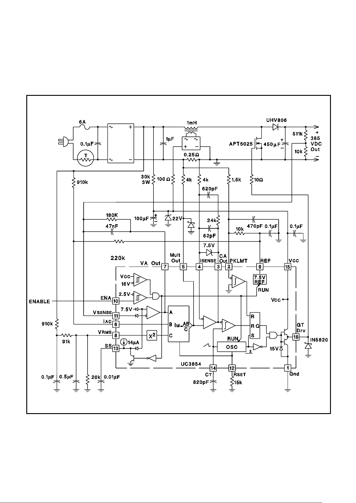
FIGURE 1 - Typical Application
NOTE: Boost inductor can be fabricated with ARNOLD MPP toroidal core part number A-438381-2, using a 55 turn primary and a
13 turn secondary.
UNITRODE CORP ORA TION
7 CONTINENTAL BLVD . • MER RIMACK, NH 03054
TEL. (603) 424-2410 FAX (603) 424-3460
These product s conta in patented circuitry and are sold unde r license from Pioneer M agnet ics, Inc.
This diag ra m de pict s a com plete 250 Watt Preregulator. At full load, this preregulator will exhibit a power fac tor of 0.99
at any power line voltage bet w een 80 and 260 V
RMS
. This sa me circuit can be us ed at higher power levels with minor
modifications to the power stage. See Design Note 39B and Application Note U-134 for further details.
UC1854
UC2854
UC3854
UDG- 92 056 - 1
8

IMPORTANT NOTICE
T exas Instruments and its subsidiaries (TI) reserve the right to make changes to their products or to discontinue
any product or service without notice, and advise customers to obtain the latest version of relevant information
to verify, before placing orders, that information being relied on is current and complete. All products are sold
subject to the terms and conditions of sale supplied at the time of order acknowledgement, including those
pertaining to warranty, patent infringement, and limitation of liability.
TI warrants performance of its semiconductor products to the specifications applicable at the time of sale in
accordance with TI’s standard warranty. Testing and other quality control techniques are utilized to the extent
TI deems necessary to support this warranty. Specific testing of all parameters of each device is not necessarily
performed, except those mandated by government requirements.
CERT AIN APPLICATIONS USING SEMICONDUCTOR PRODUCTS MAY INVOLVE POTENTIAL RISKS OF
DEATH, PERSONAL INJURY, OR SEVERE PROPERTY OR ENVIRONMENTAL DAMAGE (“CRITICAL
APPLICATIONS”). TI SEMICONDUCTOR PRODUCTS ARE NOT DESIGNED, AUTHORIZED, OR
WARRANTED TO BE SUITABLE FOR USE IN LIFE-SUPPORT DEVICES OR SYSTEMS OR OTHER
CRITICAL APPLICATIONS. INCLUSION OF TI PRODUCTS IN SUCH APPLICA TIONS IS UNDERSTOOD T O
BE FULLY AT THE CUSTOMER’S RISK.
In order to minimize risks associated with the customer’s applications, adequate design and operating
safeguards must be provided by the customer to minimize inherent or procedural hazards.
TI assumes no liability for applications assistance or customer product design. TI does not warrant or represent
that any license, either express or implied, is granted under any patent right, copyright, mask work right, or other
intellectual property right of TI covering or relating to any combination, machine, or process in which such
semiconductor products or services might be or are used. TI’s publication of information regarding any third
party’s products or services does not constitute TI’s approval, warranty or endorsement thereof.
Copyright 1999, Texas Instruments Incorporated
 Loading...