

Datasheet UC3834Q, UC3834QTR, UC3834N, UC3834J, UC3834DWTR Datasheet (Texas Instruments)
...
High Efficiency Linear Regulator
UC1834
UC2834
UC3834
FEATURES
• Minimum VIN - VOUT Less Than
0.5V At 5A Load With External
Pass Device
• Equally Usable For Either Positive
or Negative Regulator Design
• Adjustable Low Threshold Current
Sense Amplifier
• Under And Over-Voltage Fault Alert
With Programmable Delay
• Over-Voltage Fau lt Latch With
100mA Crowbar Drive Output
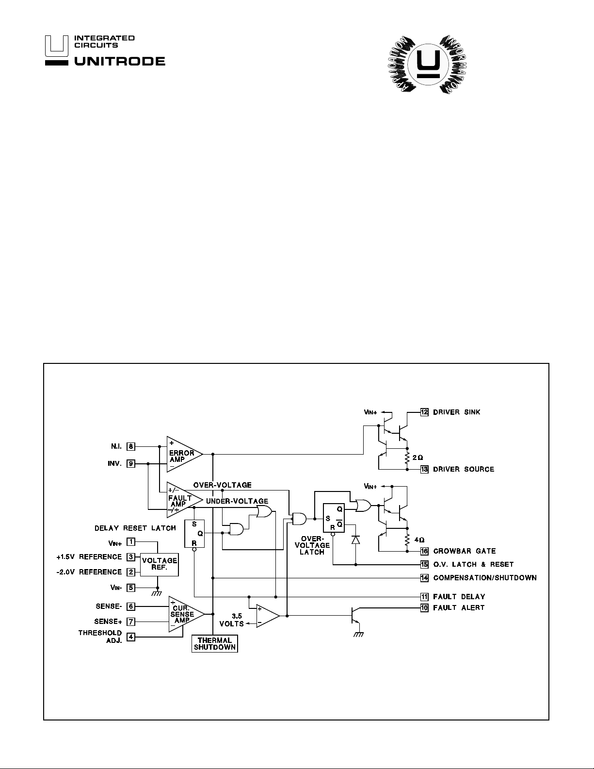
BLOCK DIAGRA M
DESCRIPTI ON
The UC1834 family of integrated circuits is optimized for the design of low
input-output differen tial linear regulators. A high gain amplifier and 200mA
sink or source drive outputs facilitate high output current designs which use
an external pass devi ce. With both positive and negative precision references, either polarity of regulator can be implemented. A current sense amplifier with a low, adjustable, threshold can be used to sense and limit
currents in either the positive or negative supply lines.
In addition, this series of parts has a fault monitoring circuit which senses
both under and ove r-voltage fault conditions. After a user defined delay for
transient reje ction, this circuitry provides a fault alert output for either fault
condition. In the over-voltage case, a 100mA crowbar output is activated.
An over-voltage latch will maintain the crowb ar output and can be used to
shutdown the driver outputs. System control to the device can be accommodated at a single input which will act as both a supply reset and remote
shutdown terminal. These die are protected against excessive power dissipation by an internal thermal shutdown function.
6/94
ABSOLUTE MAXI MUM RATING S (Note 1)
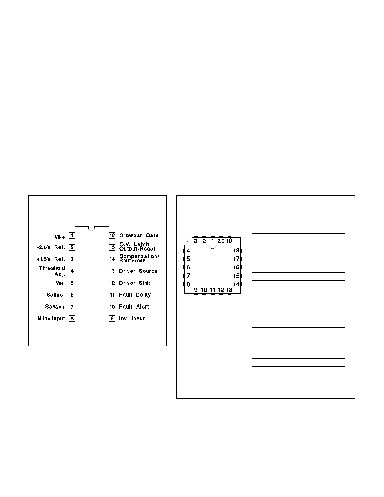
PACKAGE PIN FUNCTION
FUNCTION PIN
N/C 1
VIN + 2
−2.0V REF 3
+1.5V REF 4
Threshold Adjus t 5
N/C 6
VIN− 7
Sense− 8
Sense+ 9
N.Inv. I nput 10
N/C 11
Inv. Input 12
Fault Alert 13
Fault Delay 14
Driver Sink 15
N/C 16
Driver Source 17
Compensa tion / Shutd own 18
O.V. Latch Output/Reset 19
Crowbar Gate 20
Input Supply Voltage, VIN + . . . . . . . . . . . . . . . . . . . . . . . . . 40V
Driver Current. . . . . . . . . . . . . . . . . . . . . . . . . . . . . . . . . 400mA
Driver Sourc e to Sink Voltag e . . . . . . . . . . . . . . . . . . . . . . . 40V
Crowbar Current. . . . . . . . . . . . . . . . . . . . . . . . . . . . . . −200m A
+1.5V Ref ere nce Out pu t Cur re nt . . . . . . . . . . . . . . . . . . −10mA
Fault Alert Vo ltage . . . . . . . . . . . . . . . . . . . . . . . . . . . . . . . . 40V
Fault Alert Cu rr ent . . . . . . . . . . . . . . . . . . . . . . . . . . . . . . 15mA
Error Amplifier Inputs . . . . . . . . . . . . . . . . . . . . . . −0. 5V to 35V
Current Sense Inp ut s . . . . . . . . . . . . . . . . . . . . . . −0.5V to 40V
O.V. Latch Out pu t Voltage . . . . . . . . . . . . . . . . . . −0.5V t o 40V
O.V. Latch Output Current . . . . . . . . . . . . . . . . . . . . . . . . 15mA
CONNECTION DIAGRAMS
DIL-16, SOIC- 16 (T O P VIEW)
J or N Package, DW Package
PLCC-20, LCC-20 (TOP VIEW)
Q, L Packages
UC1834
UC2834
UC3834
Power Dissipation at T
Power Dissipation at T
Operating Jun ctio n Tem per atur e. . . . . . . . . . −55°C to +150°C
Storage Temperature. . . . . . . . . . . . . . . . . . . −65°C to +150°C
Lead Temperat ur e (sold ering , 10 secon ds). . . . . . . . . . . 300°C
Note 1: Volta ges are re fe ren ce t o V
Currents are positiv e into , negat ive out of th e specifi ed
terminals.
Consult Packag in g sect ion of Dat abo ok f or therm a l
limitations and cons id era tion s of packa ge.
A = 25°C . . . . . . . . . . . . . . . . . . 1000mW
C = 25°C. . . . . . . . . . . . . . . . . . 2000mW
IN
−
, Pin 5.
2
UC1834
UC2834
UC3834
ELECTRICAL CHARACTERISTICS:
PARAMETER TEST CONDITIONS
Turn-on Charact er is tics
Standby Supply Curre nt 5.5 7 5.5 10 m A
+1.5 Volt Reference
Output Volt age T
Line Regulatio n V
Load Regulation I
-2.0 Volt Referen ce (No te 2)
Output Volt age ( Referenced
+
to V
IN
)
Line Regulatio n V
Output Impedance 2.3 2.3 kΩ
Error Amplifier Section
Input Offs et Vo lta ge V
Input Bias Cur rent V
Input Offs et Cu rr ent V
Small Signal Open Loop Gain Output @ Pin 14, Pin 12 = V
CMRR V
PSRR V
Driver Sectio n
Maximum Output Current 200 350 200 350 mA
Saturation Volta ge I
Output Leakage Cu rrent Pin 12 = 35V, Pin 13 = V
Shutdown Input Volta ge
at Pin 14
Shutdown In put Current
at Pin 14
Thermal Shutdown (Note 3) 165 165 °C
Fault Amplifier Sect i on
Under- and Over-Voltage
Fault Threshold
Common Mode Sen sitivit y V
Supply Sensitivity V
Fault Delay 30 45 60 30 45 60 ms/µF
Fault Alert Out put Current 2 5 2 5 mA
Fault Alert Satur ation Voltage I
O.V. Latc h Out put Curr ent 2 4 2 4 mA
O.V. Latch Satura tion Voltag e I
O.V. Latch Out put Reset
Voltage
Crowbar Gate Current −100 −175 −100 −175 mA
Crowbar Gate Leakage
Current
Note 2: When using both th e 1.5V and −2.0V references t he cur rent out of pin 3 should be bala nced by an equivalent cur ren t into
−
Pin 2. The
2.0V outp ut will change −2.3mV per µA of imbalance.
Note 3: Thermal shut down turns off the drive r . If Pin 15 (O.V. Lat ch Out put ) is tied to P in 14 (Compe nsat ion/ Shu td own) the
O.V. Latch will be reset.
J = 25°C 1.485 1.5 1.515 1.47 1.5 1.53 V
T
J(MIN
IN+ = 5 to 35V 1 10 1 15 mV
OUT = 0 to 2mA 1 10 1 15 mV
J
= 25°C −2.04 −2 −1.96 −2.06 −2 −1.94 V
T
T
J(MIN) ≤ TJ ≤ TJ(MAX) −2.06 −1.94 −2.08 −1.92
IN+ = 5 to 35V 1.5 15 1.5 20 mV
CM = 1.5V 1 6 1 10 mV
CM = 1.5V −1 −4 −1 −8 µA
CM = 1.5V 0.1 1 0.1 2 µA
Pin 13, 20Ω to VIN−
CM = 0.5 to 33V, V
IN+ = 5 to 35V, VCM = 1.5V 70 100 70 100 dB
OUT = 100mA 0.5 1.2 0.5 1.5 V
I
OUT ≤ 100µA, Pin 13 = VIN−, Pin 12 =
V
IN+
Pin 14 = V
IOUT ≤ 100µA, Pin 13 = VIN−
CM = 1.5V, @ E/A I n puts 120 150 180 110 150 190 mV
V
IN+ = 35V, VCM = 1.5 to 33V −0.4 −0.8 −0.4 −1.0 %/v
CM = 1.5V, VIN+ = 5 to 35V −0.5 −1.0 −0.5 −1.2 %/V
OUT = 1mA 0 .2 0.5 0.2 0.5 V
OUT = 1mA 1 .0 1.3 1.0 1.3 V
V
IN+ = 35V, Pin 16 = VIN− −0.5 −50 −0.5 −50 µA
Unless otherwise stated, these specifications apply for TA=−55°C to +125°C
for the UC1834, −40°C to +85°C for the UC2834, and 0°C to +70°C for the
UC3834. V
≤ TJ ≤ TJ(MAX) 1.47 1.53 1.455 1.545
)
IN−, Pin 12 = VIN+
IN+ = 15V , V IN− = 0V, TA = TJ.
UC1834
UC3834 UNITS
UC2834
MIN TYP MAX MIN TYP MAX
IN+
+
= 35V 60 80 60 80 dB
IN
IN−, Pin 14 = VIN− 0.1 50 0.1 50 µA
50 65 50 65 dB
0.4 1 0.4 1 V
−100 −150 −100 −150 µA
0.3 0.4 0.6 0.3 0.4 0.6 V
3

UC1834
UC2834
UC3834
ELECTRICAL CHARACTERISTICS:
Unless otherwise stated, these specifications apply for TA=−55°C to +125°C
for the UC1834, −40°C to +85°C for the UC2834, and 0°C to +70°C for the
UC3834. V
PARAMETER TEST CONDITIONS
Current Sense Amplifier Section
Threshold Volt age Pin 4 Open, V
Pin 4 = 0.5V, V
Threshold Sup ply Sensit ivity Pin 4 Open, V
Adj. Input Cur ren t Pin 4 = 0.5V −2 −10 −2 −10 µA
Sense Inpu t Bias Current V
CM = VIN+ 100 200 100 200 µA
V
CM = VIN−−100 −200 −100 −200
CM = VIN+ or VIN− 130 150 170 120 150 180 mV
CM
CM = VIN−, VIN+ = 5 to 35V −0.1 −0.3 −0.1 −0.5 %/V
Current Sense Th reshold Adj ust ment
IN+ = 15V , V IN− = 0V. TA = TJ
UC1834
UC2834
MIN TYP MAX MIN TYP MAX
= VIN+ or VIN− 40 50 60 30 50 70
UC3834 UNITS
Current Limiting Knee Characteristics
Error Amplifier Gain and Phase
Frequency Response
Differential Voltage at Curren t Sense
Inputs - mV (reference to sense − input)
Current Sense Amplifier Gai n an d Ph as e
Frequency Respo n s e
4

APPLICATION INF ORMATI ON
UC1834
UC2834
UC3834
Foldback Current Limiti n g
Both the curren t sense and error ampl ifie rs on the UC1834
are tran scondu ctan ce type a mpli fier s. A s a resu lt, their v olt age gain is a direct func tion of the load impedance at their
shared output pin, Pin 14. Their small signal voltage gain as
a function of load and frequency is nominally given by;
Z
L
A
V E
for: f
⁄
A
≤
(f)
=
700
and A
Ω
500kHz and |ZL(f)| ≤ 1 M
V C. S
Z
L
=
(f)
70Ω
. ⁄
A
Ω
Where:
A
V=Small Sign al Volta ge G ain t o pi n 1 4.
Z
L(f) = Load Impedance at Pin 14.
The UC1834 fault delay circuitry prevents the fault outputs
from responding to transient fault conditions. The delay reset
latch insures that the f ull, use r def ined, delay pass es befo re an
over-voltage fault respon se occurs. This p reven ts un necessa ry
crowbar, or latched-off conditions, from occurring following
sharp under-voltage to over-voltage transients.
Setting the Thresho l d Adju st Vo lt age ( V
The crowbar output on the UC1834 is activated following a
sustained over-voltage condition. The crowbar output remains
high as long as the fault condition persists, or, as long as the
over-voltage latch is set. The latch is set with an over-voltage
fault if the voltage at Pin 15 is above the latch reset threshold,
typically 0.4V. When the latch is set, its Q− output will pull Pin
15 low through a series diode. As long as a nominal pull-up
load exists, the series diode prevents Q− from pulling Pin 15
below the reset threshold. However, Pin 15 is pulled low
enough to disable the driver outputs if Pins 15 and 14 are
tied together. With Pin 15 and 14 common, the regulator
will latch off in response to an over-voltage fault. If the
fault condition is cleared and Pins 14 and 15 are momentarily pulled below the latch reset threshold, the driver outputs are re-enabled.
ADJ)
5

TYPICAL APPLICATIONS
UC1834
UC2834
UC3834
5-10 Amp Positive Regulator
5-10 Amp Negative Regulator
UNITRODE CORPORATION
7 CONTINENTAL BLVD. • MERRIMACK, NH 03054
TEL. (603) 424-2410 • FAX (603) 424-3460
6

IMPORTANT NOTICE
T exas Instruments and its subsidiaries (TI) reserve the right to make changes to their products or to discontinue
any product or service without notice, and advise customers to obtain the latest version of relevant information
to verify, before placing orders, that information being relied on is current and complete. All products are sold
subject to the terms and conditions of sale supplied at the time of order acknowledgement, including those
pertaining to warranty, patent infringement, and limitation of liability.
TI warrants performance of its semiconductor products to the specifications applicable at the time of sale in
accordance with TI’s standard warranty. Testing and other quality control techniques are utilized to the extent
TI deems necessary to support this warranty . Specific testing of all parameters of each device is not necessarily
performed, except those mandated by government requirements.
CERTAIN APPLICA TIONS USING SEMICONDUCT OR PRODUCTS MAY INVOLVE POTENTIAL RISKS OF
DEATH, PERSONAL INJURY, OR SEVERE PROPERTY OR ENVIRONMENTAL DAMAGE (“CRITICAL
APPLICATIONS”). TI SEMICONDUCTOR PRODUCTS ARE NOT DESIGNED, AUTHORIZED, OR
WARRANTED TO BE SUITABLE FOR USE IN LIFE-SUPPORT DEVICES OR SYSTEMS OR OTHER
CRITICAL APPLICA TIONS. INCLUSION OF TI PRODUCTS IN SUCH APPLICATIONS IS UNDERST OOD TO
BE FULLY AT THE CUSTOMER’S RISK.
In order to minimize risks associated with the customer’s applications, adequate design and operating
safeguards must be provided by the customer to minimize inherent or procedural hazards.
TI assumes no liability for applications assistance or customer product design. TI does not warrant or represent
that any license, either express or implied, is granted under any patent right, copyright, mask work right, or other
intellectual property right of TI covering or relating to any combination, machine, or process in which such
semiconductor products or services might be or are used. TI’s publication of information regarding any third
party’s products or services does not constitute TI’s approval, warranty or endorsement thereof.
Copyright 1999, Texas Instruments Incorporated
 Loading...