

Datasheet UC3610QTR, UC3610N, UC3610Q, UC3610DWTR, UC3610DW Datasheet (Texas Instruments)
...
UC1610
UC2610
UC3610
DESCRIPTION
This eight-diode array is designed for high-current, low duty-cycle applications
typical of flyback voltage clamping for inductive loads. The dual bridge connection
makes this device particularly applicable to bipolar driven stepper motors.
The use of Schottky diode technology features high efficiency through lowered forward voltage drop and decreased reverse recovery time.
This single monolithic chip is fabricated in both hermetic CERDIP and copperleaded plastic packages. The UC1610 in ceramic is designed for -55°C to +125°C
environments but with reduced peak current capability. The UC2610 in plastic and
ceramic is desi gned for -25°C to +125°C environments also with reduced peak
current capability; while the UC3610 in plastic has higher current rating over a 0°C
to +70°C temperature range.
Dual Schottky Diode Bridge
FEATURES
• Monolithic Eight-Diode Array
• Exceptional Efficiency
• Low Forward Voltage
• Fast Recovery Time
• High Peak Current
• Small Size
ABSOLUTE MAXIMUM RATINGS
Peak Inverse Voltage (per diode) . . . . . . . . . . . . . . . . . . . . . . . . . . . . . . . . . . . . . . . . . . . 50V
Peak Forward Current
UC1610 . . . . . . . . . . . . . . . . . . . . . . . . . . . . . . . . . . . . . . . . . . . . . . . . . . . . . . . . . . . . . . 1A
UC2610 . . . . . . . . . . . . . . . . . . . . . . . . . . . . . . . . . . . . . . . . . . . . . . . . . . . . . . . . . . . . . . 1A
UC3610 . . . . . . . . . . . . . . . . . . . . . . . . . . . . . . . . . . . . . . . . . . . . . . . . . . . . . . . . . . . . . . 3A
Power Dissipation at T
A = +70°C . . . . . . . . . . . . . . . . . . . . . . . . . . . . . . . . . . . . . . . . . . . 1W
Storage Tempe rature Rang e. . . . . . . . . . . . . . . . . . . . . . . . . . . . . . . . . . . . -65°C to +150°C
Lead Temperat ure (Solde ring, 10 Sec onds ). . . . . . . . . . . . . . . . . . . . . . . . . . . . . . . . . 300°C
Note: Consult Packaging Sec tion of Databook f or the rmal limitations and con sider at ions of
package.
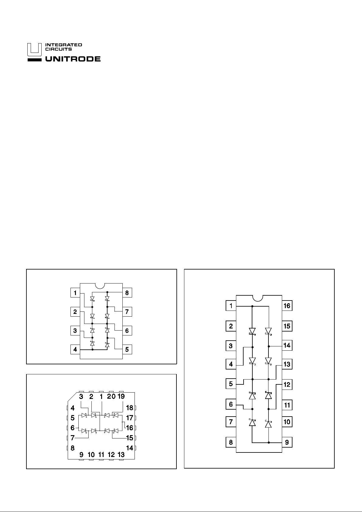
CONNECTION DIAGRAMS
SOIC-16 (TOP VIEW)
DW Package
DIL-8 (TOP VIEW)
N or J Package
PLCC-20 (TOP VIEW)
Q Package
3/95
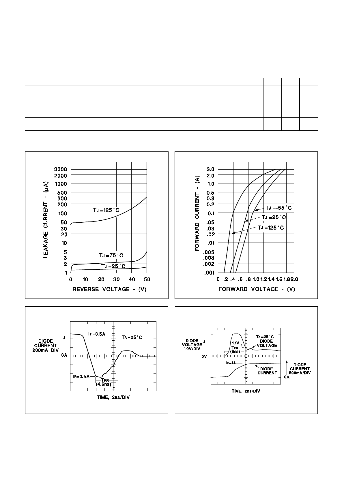
PARAMETER TEST CONDITIONS MIN TYP MAX UNITS
Forward Voltage Dro p I
F = 100mA 0.35 0.5 0.7 V
I
F = 1A 0.8 1.0 1.3 V
Leakage Current V
R = 40V .01 0.1 mA
V
R = 40V, TJ = +100°C 0.1 1.0 mA
Reverse Recovery 0.5A Forward to 0.5A Revers e 15 ns
Forward Recovery 1A Forward to 1.1V Recovery 30 ns
Junction Capacitance V
R = 5V 70 pF
Note: At forward curre nt s of grea te r than 1.0A a parasit ic current of appr oxim at ely 10m A may be collected by adjacent diodes.
UC1610
UC2610
UC3610
ELECTRICAL CHARACTERISTICS:
All specifications ap ply to each individu al diode. TJ = 25°C except as noted. TA = TJ.
UNITRODE INTEGRATED CIRCUITS
7 CONTINENTAL BLVD. • MERRI MACK , NH 0305 4
TEL. (603) 424-2410 • FAX (603) 424-3460
Reverse Current vs V oltage Forward Curren t vs Voltage
Forward Recovery CharacteristicsReverse Recovery Characteristics
2

IMPORTANT NOTICE
T exas Instruments and its subsidiaries (TI) reserve the right to make changes to their products or to discontinue
any product or service without notice, and advise customers to obtain the latest version of relevant information
to verify, before placing orders, that information being relied on is current and complete. All products are sold
subject to the terms and conditions of sale supplied at the time of order acknowledgement, including those
pertaining to warranty, patent infringement, and limitation of liability.
TI warrants performance of its semiconductor products to the specifications applicable at the time of sale in
accordance with TI’s standard warranty. Testing and other quality control techniques are utilized to the extent
TI deems necessary to support this warranty. Specific testing of all parameters of each device is not necessarily
performed, except those mandated by government requirements.
CERT AIN APPLICATIONS USING SEMICONDUCT OR PRODUCTS MAY INVOLVE POTENTIAL RISKS OF
DEATH, PERSONAL INJURY, OR SEVERE PROPERTY OR ENVIRONMENTAL DAMAGE (“CRITICAL
APPLICATIONS”). TI SEMICONDUCTOR PRODUCTS ARE NOT DESIGNED, AUTHORIZED, OR
WARRANTED TO BE SUITABLE FOR USE IN LIFE-SUPPORT DEVICES OR SYSTEMS OR OTHER
CRITICAL APPLICATIONS. INCLUSION OF TI PRODUCTS IN SUCH APPLICA TIONS IS UNDERSTOOD T O
BE FULLY AT THE CUSTOMER’S RISK.
In order to minimize risks associated with the customer’s applications, adequate design and operating
safeguards must be provided by the customer to minimize inherent or procedural hazards.
TI assumes no liability for applications assistance or customer product design. TI does not warrant or represent
that any license, either express or implied, is granted under any patent right, copyright, mask work right, or other
intellectual property right of TI covering or relating to any combination, machine, or process in which such
semiconductor products or services might be or are used. TI’s publication of information regarding any third
party’s products or services does not constitute TI’s approval, warranty or endorsement thereof.
Copyright 1999, Texas Instruments Incorporated
 Loading...