

Datasheet UC3525BN, UC3525BDWTR, UC3525BDW, UC3527BN, UC2525BDWTR Datasheet (Texas Instruments)
...
Regulating Pulse Width Modulators
UC1525B UC1527B
UC2525B UC2527B
UC3525B UC3527B
FEATURES
• 8 to 35V Operation
• 5.1V Buried Zener Reference
Trimmed to ±0.75%
• 100Hz to 500kHz Oscillator
Range
• Separate Oscillator Sync
Terminal
• Adjustable Deadtime Control
• Internal Soft-Start
• Pulse-by-Pulse Shutdown
• Input Undervoltage Lockout with
Hysteresis
• Latching PWM to Prevent
Multiple Pulses
• Dual Source/Sink Output Drivers
• Low Cross Conduction Output
Stage
• Tighter Reference Specifications
DESCRIPTION
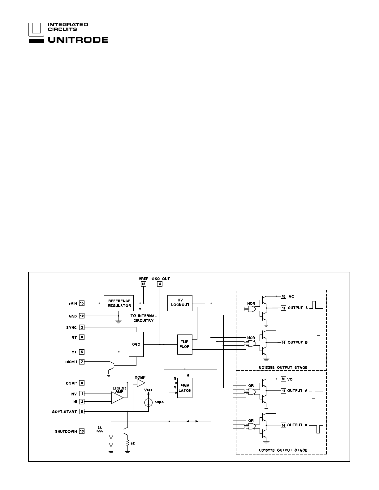
The UC1525B/1527B series of pulse width modulator integrated circuits are
designed to offer improved performance and lowered external parts count when
used in designing all types of switching power supplies. The on-chip +5.1V
buried zener reference is trimmed to ±0.75% and the input common-mode range
of the error amplifier includes the reference voltage, eliminating external resistors. A sync input to the oscillator allows multiple units to be slaved or a single
unit to be synchronized to an external system clock. A single resistor between
the CT and the discharge terminals provide a wide range of dead time adjustment.These devices also feature built-in soft-start circuitry with only an external
timing capacitor required.A shutdown terminal controls both the soft-start circuitry and the output stages, providing instantaneous turn off through the PWM
latch with pulsed shutdown, as well as soft-start recycle with longer shutdown
commands. These functions are also controlled by an undervoltage lockout
which keeps the outputs off and the soft-start capacitor discharged for sub-normal input voltages. This lockout circuitry includes approximately 500mV of hysteresis for jitter-free operation.Another feature of these PWM circuits is a latch
following the comparator.Once a PWM pulse has been terminated for any reason, the outputs will remain off for the duration of the period.The latch is reset
with each clock pulse.The output stages are totem-pole designs capable of
sourcing or sinking in excess of 200mA.The UC1525B output stage features
NOR logic, giving a LOW output for an OFF state. The UC1527B utilizes OR
logic which results in a HIGH output level when OFF.
BLOCK DIAGRAM
7/95
UDG-95055
ABSOLUTE MAXIMUM RATINGS
Supply V oltage, (+VIN) . . . . . . . . . . . . . . . . . . . . . . . . . . . .+40V
Collector Supply Voltage (VC) . . . . . . . . . . . . . . . . . . . . . .+40V
Logic Inputs . . . . . . . . . . . . . . . . . . . . . . . . . . . .−0.3V to +5.5V
Analog Inputs . . . . . . . . . . . . . . . . . . . . . . . . . . . . .−0.3V to VIN
Output Current, Source or Sink . . . . . . . . . . . . . . . . . . .500mA
Reference Output Current . . . . . . . . . . . . . . . . . . . . . . . . .50mA
Oscillator Charging Current . . . . . . . . . . . . . . . . . . . . . . . .5mA
Power Dissipation at TA = +25°C . . . . . . . . . . . . . . . . .1000mW
Power Dissipation at TC = +25°C . . . . . . . . . . . . . . . . .2000mW
Operating Junction Temperature . . . . . . . . . . .−55°C to +150°C
Storage Temperature Range . . . . . . . . . . . . . .−65°C to +150°C
Lead Temperature (Soldering, 10 sec.) . . . . . . . . . . . . .+300°C
All currents are positive into, negative out of the specified terminal.
Consult Packaging Section of Databook for thermal limitations
and considerations of packages.
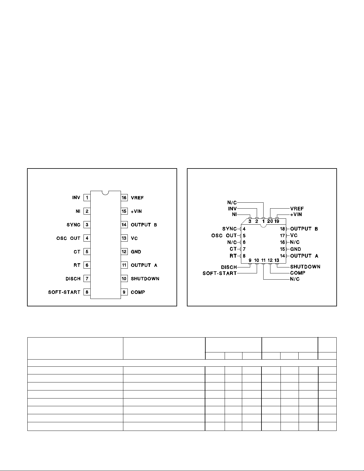
CONNECTION DIAGRAMS
UC1525B UC1527B
UC2525B UC2527B
UC3525B UC3527B
RECOMMENDED OPERATING CONDITIONS
(Note 1)
Input V oltage (+VIN) . . . . . . . . . . . . . . . . . . . . . . . .+8V to +35V
Collector Supply Voltage (VC) . . . . . . . . . . . . . . .+4.5V to +35V
Sink/Source Load Current (steady state) . . . . . . . . .0 to 100mA
Sink/Source Load Current (peak) . . . . . . . . . . . . . .0 to 400mA
Reference Load Current . . . . . . . . . . . . . . . . . . . . . .0 to 20mA
Oscillator Frequency Range . . . . . . . . . . . . . .100Hz to 400kHz
Oscillator Timing Resistor . . . . . . . . . . . . . . . . . .2kΩ to 150kΩ
Oscillator Timing Capacitor . . . . . . . . . . . . . . .0.001µF to 0.1µF
Dead Time Resistor Range . . . . . . . . . . . . . . . . . . .0Ω to 500Ω
Note 1: Range over which the de vice is functional and par ame-
ter limits are guaranteed.
DIL-16,SOIC-16 (Top View)
J or N Package,DW Package
PLCC-20,LCC-20 (Top View)
Q or L Package
ELECTRICAL CHARACTERISTICS Unless otherwise stated, these specifications apply for TA = −55°C to +125°C for the
UC1525B and UC1527B;−40°C to +85°C for the UC2525B and UC2527B;0°C to +70°C for the UC3525B and UC3527B;+VIN =
20V, TA = TJ.
UC1525B/UC2525B UC3525B
UC1527B/UC2527B UC3527B
PARAMETER TEST CONDITIONS MIN TYP MAX MIN TYP MAX UNIT
Reference Section
Output V oltage TJ = 25°C 5.062 5.10 5.138 5.036 5.10 5.164 V
Line Regulation VIN = 8V to 35V 5 10 5 10 mV
Load Regulation IL = 0mA to 20mA 7 15 7 15 mV
Temperature Stability (Note 2) Over Operating Range 10 50 10 50 mV
Total Output Variation Line, Load, and Temperature 5.036 5.164 5.024 5.176 V
Short Circuit Current VREF = 0, TJ =25°C 80 100 80 100 mA
Output Noise Voltage (Note 2) 10Hz ≤ f ≤ 10kHz, TJ = 25°C 40 200 40 200 µVrms
Long Term Stability (Note 2) T
J = 125°C, 1000 Hrs. 3 10 3 10 mV
2

UC1525B UC1527B
UC2525B UC2527B
UC3525B UC3527B
ELECTRICAL CHARACTERISTICS (cont.) Unless otherwise stated, these specifications apply for TA = −55°C to +125°C
for the UC1525B and UC1527B;−40°C to +85°C for the UC2525B and UC2527B; 0°C to +70°C for the UC3525B and UC3527B;
+VIN = 20V, TA = TJ.
UC1525B/UC2525B UC3525B
UC1527B/UC2527B UC2527B
PARAMETER TEST CONDITIONS MIN TYP MAX MIN TYP MAX UNIT
Oscillator Section (Note 3)
Initial Accuracy (Notes 2 & 3) TJ = 25°C ±2±6 ±2±6%
Voltage Stability (Notes 2 & 3) VIN = 8V to 35V ±0.3 ±1 ±1 ±2 %
Temperature Stability (Note 2) Over Operating Range ±3 ±6 ±3 ±6 %
Minimum Frequency RT = 200kΩ, CT = 0.1µF 120 120 Hz
Maximum Frequency RT = 2kΩ, CT = 470pF 400 400 kHz
Current Mirror IRT = 2mA 1.7 2.0 2.2 1.7 2.0 2.2 mA
Clock Amplitude (Notes 2 & 3) 3.0 3.5 3.0 3.5 V
Clock Width (Notes 2 & 3) TJ = 25°C 0.3 0.5 1.0 0.3 0.5 1.0 µs
Sync Threshold 1.2 2.0 2.8 1.2 2.0 2.8 V
Sync Input Current Sync Voltage = 3.5V 1.0 2.5 1.0 2.5 mA
Error Amplifier Section (VCM = 5.1V)
Input Offset Voltage 0.5 5 2 10 mV
Input Bias Current 1 10 1 10 µA
Input Offset Current 1 1 µA
DC Open Loop Gain RL ≥ 10 MegΩ 60 75 60 75 dB
Gain-Bandwidth Product (Note 2) Av = 0dB, TJ = 25°C 1 2 1 2 MHz
Output Low Level 0.2 0.5 0.2 0.5 V
Output High Level 3.8 5.6 3.8 5.6 V
Common Mode Rejection VCM = 1.5V to 5.2V 60 75 60 75 dB
Supply Voltage Rejection VIN = 8V to 35V 50 60 50 60 dB
PWM Comparator
Minimum Duty Cycle 0 0 %
Maximum Duty Cycle 45 49 45 49 %
Input Threshold (Note 3) Zero Duty Cycle 0.7 0.9 0.7 0.9 V
Input Threshold (Note3) Maximum Duty Cycle 3.3 3.6 3.3 3.6 V
Input Bias Current (Note 2) 0.05 1.0 0.05 1.0 µA
Shutdown Section
Soft Start Current V
Soft Start Low Level VSHUTDOWN = 2.5V 0.4 0.7 0.4 0.7 V
Shutdown Threshold To outputs, V
Shutdown Input Current VSHUTDOWN = 2.5V 0.4 1.0 0.4 1.0 mA
Shutdown Delay (Note 2) VSHUTDOWN = 2.5V, TJ = 25°C 0.2 0.5 0.2 0.5 µs
Output Drivers (Each Output) (VC = 20V)
Output Low Level ISINK = 20mA 0.2 0.4 0.2 0.4 V
Output HIgh Level ISOURCE = 20mA 18 19 18 19 V
Undervoltage Lockout VCOMP and VSOFTSTAR T = High 678678V
Collector Leakage VC = 35V 200 200 µA
SHUTDOWN = 0V, 25 50 80 25 50 80 µA
VSOFTSTART = 0V
SOFTST AR T = 5.1V, 0.6 0.8 1.0 0.6 0.8 1.0 V
TJ =25°C
ISINK = 100mA 1.0 2.0 1.0 2.0 V
ISOURCE = 100mA 17 18 17 18 V
3

UC1525B UC1527B
UC2525B UC2527B
UC3525B UC3527B
ELECTRICAL CHARACTERISTICS
for the UC1525B and UC1527B;−40°C to +85°C for the UC2525B and UC2527B; 0°C to +70°C for the UC3525B and UC3527B;
+VIN = 20V, TA = TJ.
PARAMETER TEST CONDITIONS MIN TYP MAX MIN TYP MAX UNIT
Output Drivers (Each Output) (VC = 20V) (cont.)
Rise Time (Note 2) CL = 1nF, TJ = 25°C 100 600 100 600 ns
Fall Time (Note 2) CL = 1nF, TJ = 25°C 50 300 50 300 ns
Cross conduction charge Per cycle, TJ = 25°C3030nc
Total Standby Current
Supply Current VIN = 35V 14 20 14 20 mA
Note 2: Guaranteed by design.Not 100% tested in production.
Note 3. Tested at fosc= 40kHz (R
f =
CT•(0.7•RT + 3RD)
1
T
= 3.6Ω, CT= 0.01µF, RD= 0Ω).Approximate oscillator frequency is defined by:
(cont.) Unless otherwise stated, these specifications apply for TA = −55°C to +125°C
UC1525B/UC2525B UC3525B
UC1527B/UC2527B UC2527B
PRINCIPLES OF OPERATION AND TYPICAL CHARACTERISTICS
UC1525B Output Circuit
(1/2 Circuit Shown)
UC1525B Output Saturation Characteristics
UDG-95056
UDG-95058
For single-ended supplies, the driver outputs are grounded.
The VC terminal is switched to ground by the totem-pole
source transistors on alternate oscillator cycles.
UDG-95057
UDG-95059
In conventional push-pull bipolar designs, forward base
drive is controlled by R1-R3.Rapid turn-off times for the
power devices are achieved with speed-up capacitors C,
and C2.
4

UC1525B UC1527B
UC2525B UC2527B
UC3525B UC3527B
UDG-95060
The low source impedance of the output drivers provides
rapid charging of power FET input capacitance while minimizing external components.
PRINCIPLES OF OPERATION AND TYPICAL
CHARACTERISTICS
Shutdown Options (See Block Diagram)
Since both the compensation and soft-start terminals
(Pins 9 and 8) have current source pull-ups, either can
readily accept a pull-down signal which only has to sink
a maximum of 100µA to turn off the outputs.This is subject to the added requirement of discharging whatever
external capacitance may be attached to these pins.
An alternate approach is the use of the shutdown circuitry of Pin 10 which has been improved to enhance the
available shutdown options. Activating this circuit by
UC1525B Oscillator Schematic
UDG-95061
Low power transformers can be driven directly by the
UC1525B.Automatic reset occurs during dead time, when
both ends of the primary winding are switched to ground.
applying a positive signal on Pin 10 performs two functions: the PWM latch is immediately set providing the
fastest turn-off signal to the external soft-start capacitor.
If the shutdown command is short, the PWM signal is
terminated without significant discharge of the soft-start
capacitor, thus, allowing, for example, a convenient
implementation of pulse-by-pulse current limiting.
Holding Pin 10 high for a longer duration, however, will
ultimately discharge this external capacitor, recycling
slow turn-on upon release.
Pin 10 should not be left floating as noise pickup could
conceivably interrupt normal operation.
UDG-95062
5

UC1525B UC1527B
UC2525B UC2527B
UC3525B UC3527B
Oscillator Charge Time vs.RT and CT Oscillator Discharge Time vs.RD and CT
UC1525B Error Amplifier
Error Amplifier Open-Loop
Frequency Response
6

LAB TEST FIXTURE
UC1525B UC1527B
UC2525B UC2527B
UC3525B UC3527B
UNITRODE INTEGRATED CIRCUITS
7 CONTINENTAL BLVD.• MERRIMACK, NH 03054
TEL.(603) 424-2410 • FAX (603) 424-3460
7

IMPORTANT NOTICE
T exas Instruments and its subsidiaries (TI) reserve the right to make changes to their products or to discontinue
any product or service without notice, and advise customers to obtain the latest version of relevant information
to verify, before placing orders, that information being relied on is current and complete. All products are sold
subject to the terms and conditions of sale supplied at the time of order acknowledgement, including those
pertaining to warranty, patent infringement, and limitation of liability.
TI warrants performance of its semiconductor products to the specifications applicable at the time of sale in
accordance with TI’s standard warranty. Testing and other quality control techniques are utilized to the extent
TI deems necessary to support this warranty . Specific testing of all parameters of each device is not necessarily
performed, except those mandated by government requirements.
CERTAIN APPLICATIONS USING SEMICONDUCTOR PRODUCTS MAY INVOLVE POTENTIAL RISKS OF
DEATH, PERSONAL INJURY, OR SEVERE PROPERTY OR ENVIRONMENTAL DAMAGE (“CRITICAL
APPLICATIONS”). TI SEMICONDUCTOR PRODUCTS ARE NOT DESIGNED, AUTHORIZED, OR
WARRANTED TO BE SUITABLE FOR USE IN LIFE-SUPPORT DEVICES OR SYSTEMS OR OTHER
CRITICAL APPLICA TIONS. INCLUSION OF TI PRODUCTS IN SUCH APPLICATIONS IS UNDERST OOD TO
BE FULLY AT THE CUSTOMER’S RISK.
In order to minimize risks associated with the customer’s applications, adequate design and operating
safeguards must be provided by the customer to minimize inherent or procedural hazards.
TI assumes no liability for applications assistance or customer product design. TI does not warrant or represent
that any license, either express or implied, is granted under any patent right, copyright, mask work right, or other
intellectual property right of TI covering or relating to any combination, machine, or process in which such
semiconductor products or services might be or are used. TI’s publication of information regarding any third
party’s products or services does not constitute TI’s approval, warranty or endorsement thereof.
Copyright 1999, Texas Instruments Incorporated
 Loading...