

UC1965
UC2965
UC3965
SLUS300A - APRIL 1999
FEATURES
•
Accessible 2.5V Precision Reference
•
0.4% Initial Reference Accuracy
•
1% Reference Accuracy over Line,
Load, and Full Temperature Range
•
Low 1mV Offset Error Amplifier
•
Supports Closed Loop Soft Start
•
2X Inverting Amplifier / Buffer Output
•
4.1V Undervoltage Lockout
•
ICC 2mA at 5V
•
8-Pin SOIC or DIL Package
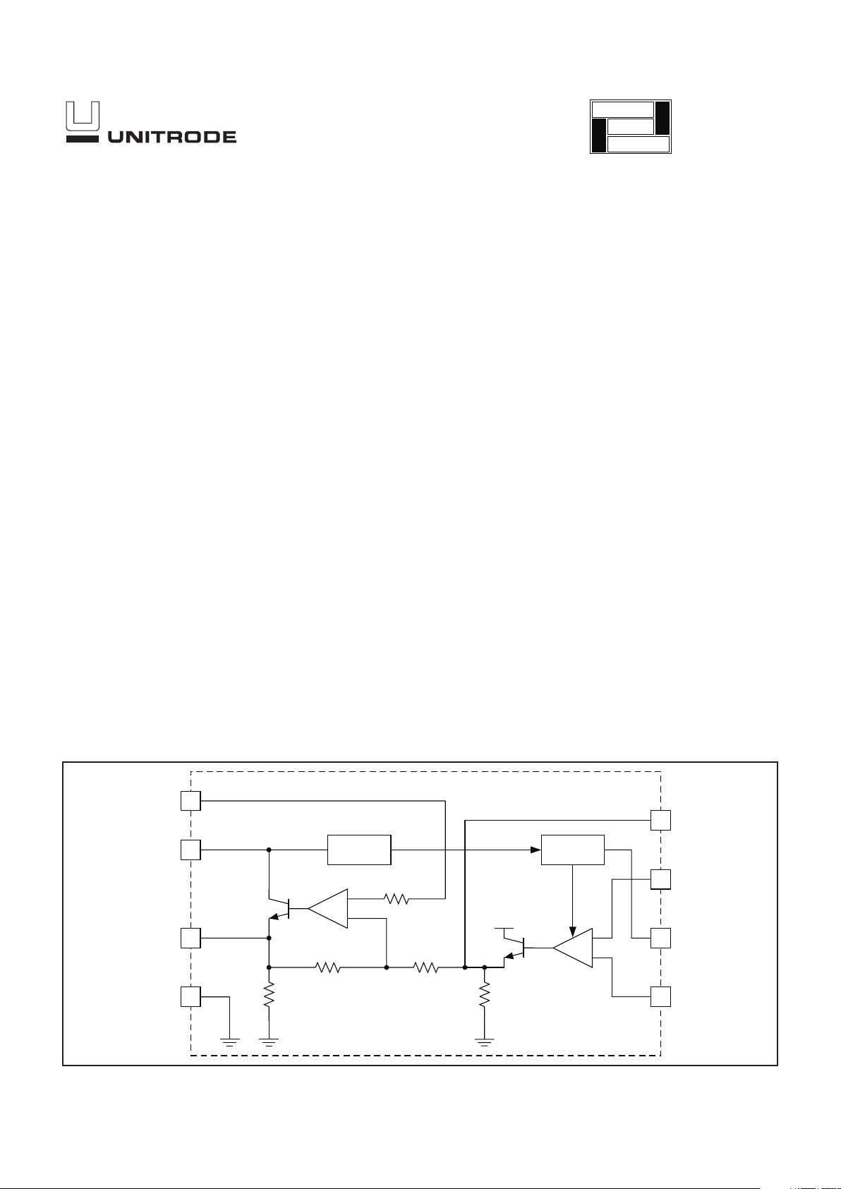
Precision Reference with Low Offset Error Amplifier
8COMP
GND
VOUT
7VFB
6VREF
5NI
1
2
3
4
VCC
OFFSET
EA
OB
UVLO
VREF
2.5V
VCC
15k
+
–
7.5k
5k
+
–
5k
2k
BLOCK DIAGRAM
UDG-98055
DESCRIPTION
The UC3965 is suitable for applications needing greater precision and
more functionality than the TL431 type shunt regulators. The wide range
VCC input capability enables the device to be biased from the secondary
side output voltage rail, resulting in closed loop soft start.
The UC3965 includes an accessible 2.5V precision reference which offers
0.4% initial and 1% reference accuracy over line, load, and full tempera
ture range with a low offset error amplifier, a 2X inverting amplifier/buffer,
and an undervoltage lockout circuit. The IC is ideally suited for applica
tions where high precision PWM power supply regulation is required.
Typically, the error amplifier is configured to compare a fraction of the to
be regulated power supply voltage to the on-chip 2.5V reference. The 2X
amplifier/buffer output is then used to drive a PWM controller or regulator.
The UC3965 is also capable of driving an optocoupler diode for isolated
applications.
application
INFO
available
2
UC1965
UC2965
UC3965
ELECTRICAL CHARACTERISTICS
Unless otherwise specified, VCC = 5V, TA=TJ.
PARAMETER TEST CONDITIONS MIN TYP MAX UNITS
General
VCC 4.3 20 V
Operating Current VCC = 5V 1.5 2 4 mA
Undervoltage Current 200 µA
Minimum Voltage to Start 3.9 4.1 4.3 V
Hysteresis 200 300 400 mV
VREF
VREF Initial Accuracy +25°C 2.49 2.5 2.51 V
VREF Over Temperature –55°C to +125°C 2.48 2.5 2.52 V
Total Output Variation Line, Load, Temperature 2.475 2.5 2.525 V
Line Regulation VCC = 4.3V to 20V 2 10 mV
Load Regulation 0µA to 500µA 2 10 mV
Short Circuit Current VREF = 0V 2 mA
Error Amplifier
Input Bias V
CM
= 2.5V 200 400 nA
Input Offset Voltage V
CM
= 2.5V 1 2 mV
Input Offset Current V
CM
= 2.5V –100 0 100 nA
Gain Bandwidth Product V
IN
= 50mV P-P (Note 1) 6 MHz
Open Loop Gain VOUT = 1V to 3.75V 80 100 dB
VREF
VFB
COMP
NI
1
2
3
4
8
7
6
5
VCC
OFFSET
VOUT
GND
CONNECTION DIAGRAM
DIL-8, SOIC-8 (Top View)
J or N Package, D Package
ABSOLUTE MAXIMUM RATINGS
VCC. . . . . . . . . . . . . . . . . . . . . . . . . . . . . . . . . . . . –0.3V to 20V
VREF. . . . . . . . . . . . . . . . . . . . . . . . . . . . . . . . . . . . –0.3V to 6V
VFB, COMP, NI, VOUT. . . . . . . . . . . . . . . . . . . . . –0.3V TO 6V
Storage Temperature . . . . . . . . . . . . . . . . . . . −65°C to +150°C
Junction Temperature. . . . . . . . . . . . . . . . . . . –55°C to +150°C
Lead Temperature (Soldering, 10 sec.) . . . . . . . . . . . . . +300°C
Currents are positive into, negative out of the specified terminal.
All voltages are with respect to ground. Consult Packaging Sec
tion of Databook for thermal limitations and considerations of
packages.
TEMPERATURE RANGE PACKAGE
UC1965J –55°C to +125°C CDIP
UC2965D –40°C to +85°C SOIC
UC2965N PDIP
UC3965D 0°C to +70°C SOIC
UC3965N PDIP
ORDERING INFORMATION

3
UC1965
UC2965
UC3965
ELECTRICAL CHARACTERISTICS
Unless otherwise specified, VCC = 5V, TA=TJ.
PARAMETER TEST CONDITIONS MIN TYP MAX UNITS
Error Amplifier Section (cont.)
Output Low Level I
OUT
= 0µA 0.8 V
I
OUT
= 100µA 1.2 V
Output High Level I
OUT
= 0µA4V
I
OUT
= –500µA4V
Short Circuit Circuit V
COMP
= 0V 8 mA
CMRR V
CM
= 1.25V to 3.75V 70 100 dB
PSRR VCC = 4.3V to 20V 70 100 dB
Rising Slew Rate 2V/µs
Falling Slew Rate 0.4 V/µs
Inverting Buffer Amplifier
Input Bias V
CM
= 2.5V 1 2 µA
Output Offset Voltage V
CM
= 2.5V –20 0 20 mV
Gain Bandwidth Product V
IN
= 50mV P-P (Note 1) 1.5 MHz
Closed Loop Gain Inverting Gain –2.04 –2 –1.96 V/V
Output Low Level I
OUT
= 0µA 0.3 V
I
OUT
= 100µA 0.5 V
Output High Level I
OUT
= 0mA 4 V
I
OUT
= –4mA 4 V
Short Circuit Circuit VOUT = 0V 18 mA
CMRR V
CM
= 1.25V to 3.75V 70 100 dB
PSRR VCC = 4.3V to 20V 70 100 dB
Rising Slew Rate 0.9 V/µs
Falling Slew Rate 0.9 V/µs
Note 1: Guaranteed by design. Not 100% tested in production.
PIN DESCRIPTIONS
COMP: The output of the error amplifier and the input to
the inverting terminal of the internal output buffer. This
pin is available to compensate the high frequency gain of
the error amplifier.
GND: The reference and power ground for the device.
NI: The non-inverting input to the error amplifier.
OFFSET: The non-inverting input to the internal output
buffer.
VCC: The power input to the device. The minimum to
maximum operating voltage is 4.3V to 20V.
VFB: The inverting terminal of the error amplifier used as
both the voltage sense input to the error amplifier and its
other compensation point.
VOUT: The emitter of the output transistor. This pin is
the output of the inverting buffer. This pin has the capa
-
bility to drive an optocoupler or a PWM controller directly.
VREF: The output of the trimmed precision reference.
This reference maintains within 1% of its initial value over
its entire line, load, and temperature range.

4
UC1965
UC2965
UC3965
UNITRODE CORPORATION
7 CONTINENTAL BLVD. • MERRIMACK, NH 03054
TEL. (603) 424-2410 • FAX (603) 424-3460
For designs requiring input-output isolation, the UC3965
is used in secondary side output voltage sensing. As
shown in Fig. 1, the precision reference and low offset
error amplifier can be used in converters, such as the
isolated flyback, where the primary side error amplifier is
not used or simply not present. In this case, the
UCC3809 is used as the primary side controller.
The precision reference of the UC3965 is tied to the
non-inverting input of the device’s internal error amplifier.
The output voltage of the converter is resistively divided
and compared to this reference at the inverting input.
This error amplifier has a low 1mV input offset voltage
that insures accurate regulation of the output. The inter
nal error amplifier drives the inverting input of the output
buffer (OB) which drives an optocoupler diode. The wide
range VCC voltage enables the device to be biased from
the secondary side output voltage rail, resulting in closed
loop soft start.
As the output voltage increases beyond its desired value,
the voltage difference at the error amplifier increases.
This results in less drive at the inverting input of the inter
nal buffer, increasing its output drive to the optocoupler.
If the application does not require input-output isolation,
this buffer could be used to drive the PWM directly.
APPLICATION INFORMATION
For additional application information biasing the
UC3965, please refer to the following publication:
[1] Application Note U-165,
Design Review: Isolated 50W
Flyback with the UCC3809 Primary Side Controller and
the UC3965 Precision Reference and Error Amplifier
,by
Lisa Dinwoodie.
ADDITIONAL INFORMATION
8
7
6
5
1
2
3
4
EA
OB
UVLO
VREF
2.5V
VCC
15k
+
–
7.5k
5k
+
–
5k
2k
–V
OUT
+V
OUT
8
7
5
6
1
2
4
3
UCC3809
+V
IN
–V
IN
FB REF
SS
RT1
RT2
VDD
OUT
GND
OFFSET
VCC
VOUT
GND
COMP
VFB
VREF
NI
Figure 1. Typical application diagram.
UDG-99080
 Loading...