

Half-Bridge Bipolar Switch
UC2950
TRUTH TABLE
Source Dri ve
Pin 2
Sink Driv e
Pin 5
Output
Pin 4
Low
Low
High
High
Low
High
Low
High
Low
Off
High
High
Note: With no load, output voltage w ill be HIG H in the OF F
state.
ABSOLUTE MAXI MUM RATING S (Note 1)
Supply Voltage Ra n ge, V C . . . . . . . . . . . . . . . . . . . . . . . . . . . . . . . . . . . . 8V to 35V
Output Voltage Range , V
O . . . . . . . . . . . . . . . . . . . . . . . . . . . . . . . -3.0V to VC+3V
Input Voltage Range, V
IN . . . . . . . . . . . . . . . . . . . . . . . . . . . . . . . . . -0.3V to +7.0 V
Peak Output Cur ren t (100 m s, 10% DC) . . . . . . . . . . . . . . . . . . . . . . . . . . . . ±4.0A
Continuous Output Curr ent. . . . . . . . . . . . . . . . . . . . . . . . . . . . . . . . . . . . . . . ±2.0A
Power Dissipation with Heat Sink. . . . . . . . . . . . . . . . . . . . . . . . . . . . . . . . . . . 15W
Power Dissipation in Free Air. . . . . . . . . . . . . . . . . . . . . . . . . . . . . . . . . . . . . . . 2W
Operating Temperature Range, T
A . . . . . . . . . . . . . . . . . . . . . . . -20°C to +100°C
Storage Temperature Range, T
S . . . . . . . . . . . . . . . . . . . . . . . . . -55°C to +125°C
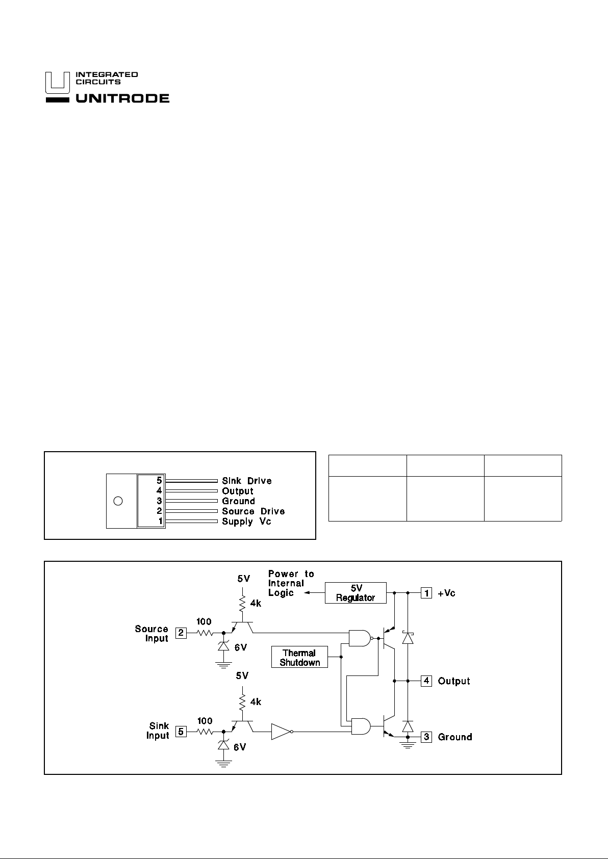
5-PIN TO-220 (TOP VIEW)
T Package
FEATURES
• Source or Sink 4.0A
• Supply Voltage to 35V
• High-Current Output Diodes
• Tri-State Operation
• TTL and CMOS Input Compatibility
• Thermal Shutdown Protection
• 300kHz Operation
• Low-Cost TO-220 Package
DESCRIPTI ON
This device i s a mono lithic integrated circui t designe d to provide high-current switching with low saturation voltages when activated by low-level logic
signals. Source and sink switches may be independently activated without
regard to timing as a b uilt-in interl ock will keep the sin k off if the source is
on.
This driver has the high current capability to drive large capacitive loads
with fast rise and fall times; but with high-speed internal flyback diodes, it is
also ideal for inductive loads. Two UC2950s can be used together to form
a full bridge, bip olar motor driver compatible with high frequency chopper
current control.
CONNECTION DIAGRAM
SIMPLIFIED SCHEMATIC
Note 1: Consult Packag in g sect ion of dat abook for thermal limit atio ns and considerations of package.
5/93
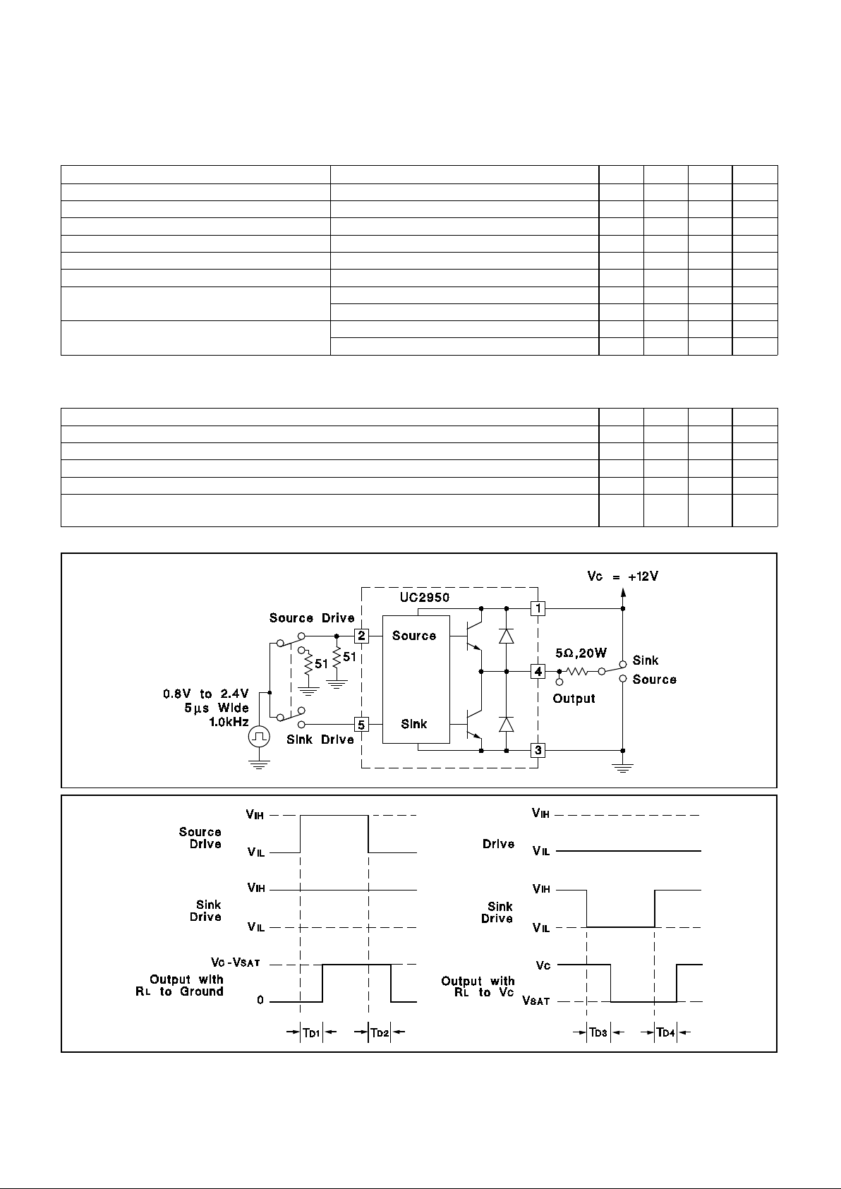
SWITCHING CHARACTERI STICS:
PARAMETERS MIN TYP MAX UNITS
Source Turn-On Delay, t
D1 300 500 ns
Source Turn-Off Delay, t
D2 1.0 2.0 µs
Sink Turn-On Delay, t
D3 200 400 ns
Sink Turn-Off Delay, t
D4 100 300 ns
Cross-Conduct ion Curr ent Spike When Source
and Sink are Activated Together
0.6 1.0 µs
ELECTRICAL CHARACTERISTICS:
PARAMETERS TEST CONDITION S MIN TYP MAX UNITS
Output Lea kage to V
C Output Off 20 500 µA
Output Lea kage to Ground Output Off -200 -500 µA
Output Sink Saturation V
OL, IL = 2.0A 1.2 2.0 V
Output Sour ce Saturation (V
C-VOL), IL = -2.0A 1.2 2.0 V
Sink Diode Forward Voltage I
D = -2.0A 1.4 2.0 V
Source Diode Forward Voltage I
D = 2.0A 1.4 2.0 V
Input Current Either Input, V
I
= 5V 20 100 µA
Either Input, V
I = 0V -1.0 -1.6 mA
Supply Current Output High 20 30 mA
Output Low 10 20 mA
UC2950
Unless otherwise stated, VC = 35V, TA = -20°C to +100 °C, V IL = 0.8V, VIH = 2.4V
for either input, TA =TJ.
See Test Circuit. V C = 12V, RL = 5Ω, TA = 25°C. Guarant eed by design , not 100%
tested in production.
SWITCHING TEST CIRCUIT
UNITRODE INTEGRATED CIRCUITS
7 CONTINENTAL BLVD. •• MERRIMACK, NH 03054
TEL. (603) 424-2410 •• FAX (603) 424-3460
2

IMPORTANT NOTICE
T exas Instruments and its subsidiaries (TI) reserve the right to make changes to their products or to discontinue
any product or service without notice, and advise customers to obtain the latest version of relevant information
to verify, before placing orders, that information being relied on is current and complete. All products are sold
subject to the terms and conditions of sale supplied at the time of order acknowledgement, including those
pertaining to warranty, patent infringement, and limitation of liability.
TI warrants performance of its semiconductor products to the specifications applicable at the time of sale in
accordance with TI’s standard warranty. Testing and other quality control techniques are utilized to the extent
TI deems necessary to support this warranty. Specific testing of all parameters of each device is not necessarily
performed, except those mandated by government requirements.
CERT AIN APPLICATIONS USING SEMICONDUCTOR PRODUCTS MAY INVOLVE POTENTIAL RISKS OF
DEATH, PERSONAL INJURY, OR SEVERE PROPERTY OR ENVIRONMENTAL DAMAGE (“CRITICAL
APPLICATIONS”). TI SEMICONDUCTOR PRODUCTS ARE NOT DESIGNED, AUTHORIZED, OR
WARRANTED TO BE SUITABLE FOR USE IN LIFE-SUPPORT DEVICES OR SYSTEMS OR OTHER
CRITICAL APPLICATIONS. INCLUSION OF TI PRODUCTS IN SUCH APPLICA TIONS IS UNDERSTOOD T O
BE FULLY AT THE CUSTOMER’S RISK.
In order to minimize risks associated with the customer’s applications, adequate design and operating
safeguards must be provided by the customer to minimize inherent or procedural hazards.
TI assumes no liability for applications assistance or customer product design. TI does not warrant or represent
that any license, either express or implied, is granted under any patent right, copyright, mask work right, or other
intellectual property right of TI covering or relating to any combination, machine, or process in which such
semiconductor products or services might be or are used. TI’s publication of information regarding any third
party’s products or services does not constitute TI’s approval, warranty or endorsement thereof.
Copyright 1999, Texas Instruments Incorporated
 Loading...