

Datasheet UC2878N, UC2875QPTR, UC2876N, UC2875QP, UC2875N Datasheet (Texas Instruments)
...
UC1875/6/7/8
UC2875/6/7/8
UC3875/6/7/8
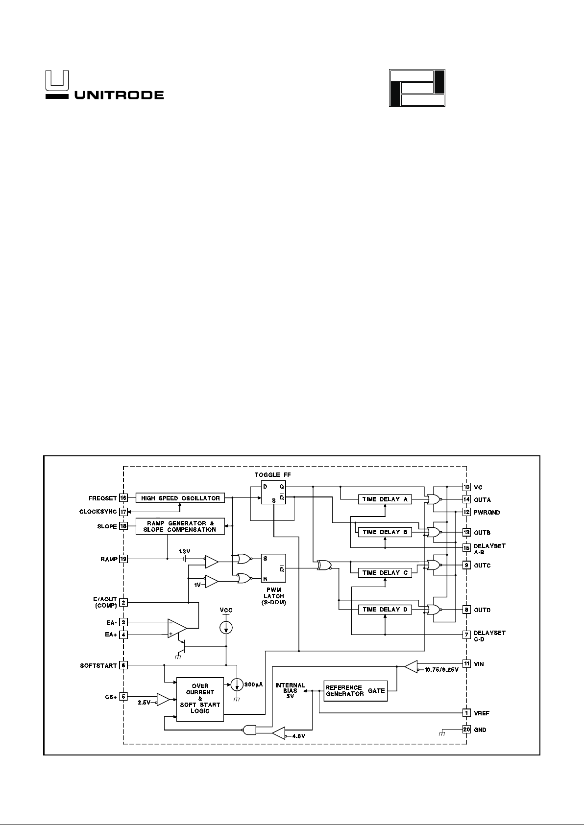
DESCRIPTION
The UC1875 family of integrated circuits implements control of a bridge
power stage by phase-shifting the switching of one half-bridge with respect
to the other, allowing constant frequency pulse-width modulation in combi
nation with resonant, zero-voltage switching for high efficiency performance
at high frequencies. This family of circuits may be configured to provide
control in either voltage or current mode operation, with a separate
over-current shutdown for fast fault protection.
A programmable time delay is provided to insert a dead-time at the turn-on
of each output stage. This delay, providing time to allow the resonant
switching action, is independently controllable for each output pair (A-B,
C-D).
With the oscillator capable of operation at frequencies in excess of 2MHz,
overall switching frequencies to 1MHz are practical. In addition to the stan
dard free running mode, with the CLOCKSYNC pin, the user may configure
these devices to accept an external clock synchronization signal, or may
lock together up to 5 units with the operational frequency determined by the
fastest device.
Protective features include an undervoltage lockout which maintains all outputs in an active-low state until the supply reaches a 10.75V threshold.
1.5V hysteresis is built in for reliable, boot-strapped chip supply.
Over-current protection is provided, and will latch the outputs in the OFF
state within 70nsec of a fault. The current-fault circuitry implements
full-cycle restart operation.
Phase Shift Resonant Controller
FEATURES
•
Zero to 100% Duty Cycle Control
•
Programmable Output Turn-On Delay
•
Compatible with Voltage or Current
Mode Topologies
•
Practical Operation at Switching
Frequencies to 1MHz
•
Four 2A Totem Pole Outputs
•
10MHz Error Amplifier
•
Undervoltage Lockout
•
Low Startup Current –150µA
•
Outputs Active Low During UVLO
•
Soft-Start Control
• Latched Over-Current Comparator
With Full Cycle Restart
• Trimmed Reference
07/99
BLOCK DIAGRAM
UDG-95073
application
INFO
available
2
UC1875/6/7/8
UC2875/6/7/8
UC3875/6/7/8
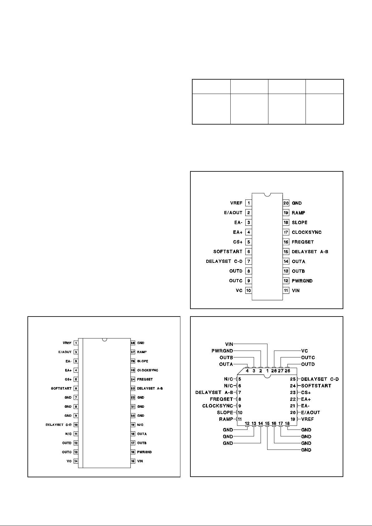
Dil-20 (Top View)
J or N Package
ABSOLUTE MAXIMUM RATINGS
Supply Voltage (VC, VIN) . . . . . . . . . . . . . . . . . . . . . . . . . . 20V
Output Current, Source or Sink
DC . . . . . . . . . . . . . . . . . . . . . . . . . . . . . . . . . . . . . . . . . 0.5A
Pulse (0.5µs). . . . . . . . . . . . . . . . . . . . . . . . . . . . . . . . . . . 3A
Analog I/0s
(Pins 1, 2, 3, 4, 5, 6, 7, 15, 16, 17, 18, 19) . . . . –0.3 to 5.3V
Storage Temperature Range . . . . . . . . . . . . . –65°C to +150°C
Junction Temperature. . . . . . . . . . . . . . . . . . . –55°C to +150°C
Lead Temperature (Soldering, 10 sec.) . . . . . . . . . . . . +300°C
Note: Pin references are to 20 pin packages.All voltages are
with respect to ground.Currents are positive into, negative out of, device terminals. Consult Unitrode
databook for information regarding thermal specifications and limitations of packages.
SOIC-28, (Top View)
DWP Package
CONNECTION DIAGRAMS
Additional features include an error amplifier with band
width in excess of 7MHz, a 5V reference, provisions for
soft-starting, and flexible ramp generation and slope com
pensation circuitry.
These devices are available in 20-pin DIP, 28-pin
“bat-wing” SOIC and 28 lead power PLCC plastic pack
ages for operation over both 0°C to 70°C and –25°C to
+85°C temperature ranges; and in hermetically sealed
cerdip, and surface mount packages for –55°C to +125°C
operation.
Device UVLO
Turn-On
UVLO
Turn-Off
Delay
Set
UC1875 10.75 9.25V Yes
UC1876 15.25V 9.25V Yes
UC1877 10.75V 9.25V No
UC1878 15.25V 9.25V No
DESCRIPTION (cont.)
PLCC-28 (Top View)
QP Package
3
UC1875/6/7/8
UC2875/6/7/8
UC3875/6/7/8
ELECTRICAL CHARACTERISTICS:
Unless otherwise stated, –55°C < TA< 125°C for the UC1875/6/7/8, –25°C < TA<
85°C for the UC2875/6/7/8 and 0°C < T
A
< 70°C for the UC3875/6/7/8, VC = VIN = 12V, R
FREQSET
= 12kΩ,C
FREQSET
= 330pF,
R
SLOPE
= 12kΩ, C
RAMP
= 200pF, C
DELAYSET A-B=CDELAYSET C-D
= 0.01µF, I
DELAYSET A-B=IDELAYSET C-D
= –500µA, TA=TJ.
PARAMETER TEST CONDITIONS MIN TYP MAX UNITS
Undervoltage Lockout
Start Threshold UC1875/UC1877 10.75 11.75 V
UC1876/UC1878 15.25 V
UVLO Hysteresis UC1875/UC1877 0.5 1.25 2.0 V
UC1876/UC1878 6.0 V
Supply Current
I
IN
Startup VIN = 8V, VC = 20V, R
SLOPE
open, I
DELAY
= 0 150 600 µA
I
C
Startup VIN = 8V, VC = 20V, R
SLOPE
open, I
DELAY
= 0 10 100 µA
I
IN
30 40 mA
I
C
15 30 mA
Voltage Reference
Output Voltage T
J
= +25°C 4.92 5 5.08 V
Line Regulation 11 < VIN < 20V 1 10 mV
Load Regulation I
VREF
= –10mA 5 20 mV
Total Variation Line, Load, Temperature 4.9 5.1 V
Noise Voltage 10Hz to 10kHz 50 µVrms
Long Term Stability T
J
= 125°C, 1000 hours 2.5 mV
Short Circuit Current VREF = 0V, T
J
= 25°C 60 mA
Error Amplifier
Offset Voltage 515mV
Input Bias Current 0.6 3 µA
AVOL 1V < V
E/AOUT
< 4V 60 90 dB
CMRR 1.5V < V
CM
< 5.5V 75 95 dB
PSRR 11V < VIN < 20V 85 100 dB
Output Sink Current V
E/AOUT
= 1V 1 2.5 mA
Output Source Current V
E/AOUT
= 4V –1.3 –0.5 mA
Output Voltage High I
E/AOUT
= –0.5mA 4 4.7 5 V
Output Voltage Low I
E/AOUT
= 1mA 0 0.5 1 V
Unity Gain BW 7 11 MHz
Slew Rate 611 V/µsec
4
UC1875/6/7/8
UC2875/6/7/8
UC3875/6/7/8
ELECTRICAL CHARACTERISTICS:
Unless otherwise stated, –55°C < TA< 125°C for the UC1875/6/7/8, –25°C < TA<
85°C for the UC2875/6/7/8 and 0°C < T
A
< 70°C for the UC3875/6/7/8, VC = VIN = 12V, R
FREQSET
= 12kΩ,C
FREQSET
= 330pF,
R
SLOPE
= 12kΩ, C
RAMP
= 200pF, C
DELAYSET A-B=CDELAYSET C-D
= 0.01µF, I
DELAYSET A-B=IDELAYSET C-D
= –500µA, TA=TJ.
PARAMETER TEST CONDITIONS MIN TYP MAX UNITS
PWM Comparator
Ramp Offset Voltage T
J
= 25°C (Note 3) 1.3 V
Zero Phase Shift Voltage (Note 4) 0.55 0.9 V
PWM Phase Shift (Note1) V
E/AOUT
> (Ramp Peak + Ramp Offset) 98 99.5 102 %
V
E/AOUT
< Zero Phase Shift Voltage 0 0.5 2 %
Output Skew (Note 1) V
E/AOUT
< 1V 5 ±20 nsec
Ramp to Output Delay UC3875/6/7/8 (Note 6) 65 100 nsec
UC1875/6/7/8, UC2875/6/7/8 (Note 6) 65 125 nsec
Oscillator
Initial Accuracy T
J
= 25°C 0.85 1 1.15 MHz
Voltage Stability 11V < VIN < 20V 0.2 2 %
Total Variation Line, Temperature 0.80 1.20 MHz
Sync Pin Threshold T
J
= 25°C 3.8 V
Clock Out Peak T
J
= 25°C 4.3 V
Clock Out Low T
J
= 25°C 3.3 V
Oscillator (cont.)
Clock Out Pulse Width R
CLOCKSYNC
= 3.9kΩ 30 100 nsec
Maximum Frequency R
FREQSET
= 5kΩ 2 MHz
Ramp Generator/Slope Compensation
Ramp Current, Minimum I
SLOPE
= 10µA, V
FREQSET
= VREF –11 –14 µA
Ramp Current, Maximum I
SLOPE
= 1mA, V
FREQSET
= VREF –0.8 –0.95 mA
Ramp Valley 0V
Ramp Peak - Clamping Level R
FREQSET
= 100kΩ 3.8 4.1 V
Current Limit
Input Bias V
CS
+ = 3V 2 5 µA
Threshold Voltage 2.4 2.5 2.6 V
Delay to Output UC3875/6/7/8 85 125 nsec
UC1875/6/7/8, UC2875/6/7/8 85 150 nsec
Soft-Start/Reset Delay
Charge Current V
SOFTSTART
= 0.5V –20 –9 –3 µA
Discharge Current V
SOFTSTART
= 1V 120 230 µA
Restart Threshold 4.3 4.7 V
Discharge Level 300 mV

5
UC1875/6/7/8
UC2875/6/7/8
UC3875/6/7/8
ELECTRICAL CHARACTERISTICS:
Unless otherwise stated, –55°C < TA< 125°C for the UC1875/6/7/8, –25°C < TA<
85°C for the UC2875/6/7/8 and 0°C < T
A
< 70°C for the UC3875/6/7/8, VC = VIN = 12V, R
FREQSET
= 12kΩ,C
FREQSET
= 330pF,
R
SLOPE
= 12kΩ, C
RAMP
= 200pF, C
DELAYSET A-B=CDELAYSET C-D
= 0.01µF, I
DELAYSET A-B=IDELAYSET C-D
= –500µA, TA=TJ.
PARAMETER TEST CONDITIONS MIN TYP MAX UNITS
Output Drivers
Output Low Level I
OUT
= 50mA 0.2 0.4 V
I
OUT
= 500mA 1.2 2.6 V
Output High Level I
OUT
= –50mA 1.5 2.5 V
I
OUT
= –500mA 1.7 2.6 V
Delay Set (UC1875 and UC1876 only)
Delay Set Voltage I
DELAY
= –500µA 2.3 2.4 2.6 V
Delay Time I
DELAY
= –250µA (Note 5) (UC3875/6/7/8,
UC2875/6/7/8)
150 250 400 nsec
I
DELAY
= –250µA (Note 5) (UC1875/6/7/8) 150 250 600 nsec
Note 1: Phase shift percentage (0% = 0°, 100% = 180°) is defined as
θ=
200
T
Φ%
, where is the phase shift, and and T are de
-
fined in Figure 1. At 0% phase shift,
is the output skew.
Note 2: Delay time is defined as delay = T (1/2–(duty cycle)), where T is defined in Fig. 1.
Note 3: Ramp offset voltage has a temperature coefficient of about –4mV/°C.
Note 4: Zero phase shift voltage has a temperature coefficient of about –2mV/°C.
Note 5: Delay time can be programmed via resistors from the delay set pins to ground.Delay time
≅
•62 5 10
12.–
I
DELAY
sec. Where
I
DELAY
=
Delay set voltage
R
DELAY
The recommended range for I
DELAY
is 25 A I
DELAY
1mA
Note 6: Ramp delay to output time is defined in Fig.2.
Figure 1
Figure 2
Duty Cycle = t/T
Period = T
T
DHL
(A to C) = T
DHL
(B to D) = Φ
Phase Shift, Output Skew & Delay Time Definitions
UDG-95075
UDG-95074

6
UC1875/6/7/8
UC2875/6/7/8
UC3875/6/7/8
CLOCKSYNC (bi-directional clock and synchroniza
-
tion pin): Used as an output, this pin provides a clock
signal. As an input, this pin provides a synchronization
point. In its simplest usage, multiple devices, each with
their own local oscillator frequency, may be connected to
gether by the CLOCKSYNC pin and will synchronize on
the fastest oscillator. This pin may also be used to syn
chronize the device to an external clock, provided the ex
ternal signal is of higher frequency than the local
oscillator. A resistor load may be needed on this pin to
minimize the clock pulse width.
E/AOUT (error amplifier output): This is is the gain
stage for overall feedback control. Error amplifier output
voltage levels below 1 volt will force 0° phase shift. Since
the error amplifier has a relatively low current drive capa
bility, the output may be overridden by driving with a suffi
ciently low impedance source.
CS+ (current sense): The non-inverting input to the cur
rent-fault comparator whose reference is set internally to
a fixed 2.5V (separate from VREF). When the voltage at
this pin exceeds 2.5V the current-fault latch is set, the
outputs are forced OFF and a SOFT-START cycle is initiated. If a constant voltage above 2.5V is applied to this
pin the outputs are disabled from switching and held in a
low state until the CS+ pin is brought below 2.5V. The
outputs may begin switching at 0 degrees phase shift before the SOFTSTART pin begins to rise -- this condition
will not prematurely deliver power to the load.
FREQSET (oscillator frequency set pin): A resistor
and a capacitor from FREQSET to GND will set the oscil
lator frequency.
DELAYSET A-B, DELAYSET C-D (output delay con
trol): The user programmed current flowing from these
pins to GND set the turn-on delay for the corresponding
output pair. This delay is introduced between turn-off of
one switch and turn-on of another in the same leg of the
bridge to provide a dead time in which the resonant
switching of the external power switches takes place.
Separate delays are provided for the two half-bridges to
accommodate differences in the resonant capacitor
charging currents.
EA– (error amplifier inverting input): This is normally
connected to the voltage divider resistors which sense
the power supply output voltage level.
EA+ (error amplifier non-inverting input): This is nor
mally connected to a reference voltage used for compari
son with the sensed power supply output voltage level at
the EA+ pin.
GND (signal ground): All voltages are measured with
respect to GND. The timing capacitor, on the FREQSET
pin, any bypass capacitor on the VREF pin, bypass ca
pacitors on VIN and the ramp capacitor, on the RAMP
pin, should be connected directly to the ground plane
near the signal ground pin.
OUTA-OUTD (outputs A-D): The outputs are 2A to
tem-pole drivers optimized for both MOSFET gates and
level-shifting transformers. The outputs operate as pairs
with a nominal 50% duty-cycle. The A-B pair is intended
to drive one half-bridge in the external power stage and
is syncronized with the clock waveform. The C-D pair will
drive the other half-bridge with switching phase shifted
with respect to the A-B outputs.
PWRGND (power ground): VC should be bypassed with
a ceramic capacitor from the VC pin to the section of the
ground plane that is connected to PWRGND. Any re
quired bulk reservoir capacitor should parallel this one.
Power ground and signal ground may be joined at a sin
gle point to optimize noise rejection and minimize DC
drops.
RAMP (voltage ramp): This pin is the input to the PWM
comparator. Connect a capacitor from here to GND. A
voltage ramp is developed at this pin with a slope:
dV
dT
SenseVoltage
RC
SLOPE RAMP
=
•
Current mode control may be achieved with a minimum
amount of external circuitry, in which case this pin provides slope compensation.
Because of the 1.3V offset between the ramp input and
the PWM comparator, the error amplifier output voltage
can not exceed the effective ramp peak voltage and duty
cycle clamping is easily achievable with appropriate val
ues of R
SLOPE
and C
RAMP
.
SLOPE (set ramp slope/slope compensation): A resis
tor from this pin to VCC will set the current used to gen
erate the ramp. Connecting this resistor to the DC input
line voltage will provide voltage feed-forward.
SOFTSTART (soft start): SOFTSTART will remain at
GND as long as VIN is below the UVLO threshold.
SOFTSTART will be pulled up to about 4.8V by an inter
nal 9µA current source when VIN becomes valid (assum
ing a non-fault condition). In the event of a current-fault
(CS+ voltage exceeding 2.5V), SOFTSTART will be
pulled to GND and them ramp to 4.8V. If a fault occurs
during the SOFTSTART cycle, the outputs will be imme
diately disabled and SOFTSTART must charge fully prior
to resetting the fault latch.
For paralleled controllers, the SOFTSTART pins may be
paralled to a single capacitor, but the charge currents will
be additive.
PIN FUNCTIONAL DESCRIPTIONS

7
UC1875/6/7/8
UC2875/6/7/8
UC3875/6/7/8
VC (output switch supply voltage): This pin supplies
power to the output drivers and their associated bias cir
-
cuitry. Connect VC to a stable source above 3V for nor
mal operation, above 12V for best performance. This
supply should be bypassed directly to the PWRGND pin
with low ESR, low ESL capacitors.
VIN (primary chip supply voltage): This pin supplies
power to the logic and analog circuitry on the integrated
circuit that is not directly associated with driving the out
put stages. Connect VIN to a stable source above 12V
for normal operation. To ensure proper chip functionality,
these devices will be inactive until VIN exceeds the upper
undervoltage lockout threshold. This pin should by by
passed directly to the GND pin with low ESR, low ESL
capacitors.
NOTE: When VIN exceeds the UVLO threshold the sup
-
ply current (I
IN
) will jump from about 100µA to a current
in excess of 20µA. If the UC1875 is not connected to a
well bypassed supply, it may immediately enter UVLO
again.
VREF: This pin is an accurate 5V voltage reference. This
output is capable of delivering about 60mA to peripheral
circuitry and is internally short circuit current limited.
VREF is disabled while VIN is low enough to force the
chip into UVLO. The circuit is also in UVLO until VREF
reaches approximately 4.75V. For best results bypass
VREF with a 0.1µF, low ESR, low ESL, capacitor to the
GND pin.
PIN FUNCTIONAL DESCRIPTIONS (cont.)
When power is applied to the circuit and VIN is below
the upper UVLO threshold, I
IN
will be below 600µA, the
reference generator will be off, the fault latch is reset,
the soft-start pin is discharged, and the outputs are actively
held low. When VIN exceeds the upper UVLO thresh
old, the reference generator turns on. All else remains
in the shut-down mode until the output of the reference,
VREF, exceeds 4.75V.
APPLICATIONS INFORMATION
UNDERVOLTAGE LOCKOUT SECTION
OSCILLATOR
The high frequency oscillator may be either
free-running or externally synchronized. For
free-running operation, the frequency is set via an ex
-
ternal resistor and capacitor to ground from the
FREQSET pin.
UDG-95078
UDG-95077
UDG-95079
UDG-95076
Simplified Oscillator Schematic

8
UC1875/6/7/8
UC2875/6/7/8
UC3875/6/7/8
APPLICATIONS INFORMATION (cont.)
SYNCHRONIZING THE OSCILLATOR
The CLOCKSYNC pin of the oscillator may be used to synchronize multiple UC1875 devices simply by connecting
the CLOCKSYNC of each UC1875 to the others:
Syncing to external TTL/CMOS
All ICs will sync to chip with the fastest local oscillator.
R1 & RN
may
be needed to keep sync pulse narrow due to capacitance on line.
R1 & RN
may
also be needed to properly terminate R
SYNC
line.
Although each UC1875/6/7/8 has a local oscillator fre
quency, the group of devices will synchronize to the
fastest oscillator driving the CLOCKSYNC pin. This ar
rangement allows the synchronizing connection be
tween ICs to be broken without any local loss of
functionality.
Synchronizing the device to an external clock signal
may be accomplished with a minimum of external cir
cuitry, as shown in the previous figure.
Capacitive loading on the CLOCKSYNC pin will in
crease the clock pulse width, and may adversely effect
system performance. Therefore, a resistor to ground
from the CLOCKSYNC pin is optional, but may be re
quired to offset capacitive loading on this pin. These re
sistors are shown in the oscillator schematics as R1,
RN.
ICs will sync to fastest chip or TTL clock if it is higher frequency.
R & RN
may
be needed for same reasons as above
UDG-95080
UDG-95081
1875/6/7/8s only

9
UC1875/6/7/8
UC2875/6/7/8
UC3875/6/7/8
In each of the output stages, transistors Q3 through Q6
form a high-speed totem-pole driver which will source
or sink more than one amp peak with a total delay of
approximately 30 nanoseconds. To ensure a low output
level prior to turn-on, transistors Q7 through Q9 form a
self-biased driver to hold Q6 on prior to the supply
reaching its turn-on threshold. This circuit is operable
when the chip supply is zero. Q6 is also turned on and
held low with a signal from the fault logic portion of the
chip.
APPLICATIONS INFORMATION (cont.)
DELAY BLOCKS AND OUTPUT STAGES
The delay providing the dead-time is accomplished with
C1 which must discharge to V
TH
before the output can
go high. The time is defined by the current sources, I1,
which is programmed by an external resistor, R
TD
. The
voltage on the Delay Set pins is internally regulated to
2.5V and the range of dead time control is
from 50 to 200 nanoseconds. NOTE: There is no way
to disable the delay circuitry, and the delay time must
be programmed.
The four outputs of the UC1875/6/7/8 interface to the full bridge converter switches as shown below:
OUTPUT SWITCH ORIENTATION
UDG-95083
UDG-95082
3 Winding Bifilar, AWG 30 Kynar Insulation

10
UC1875/6/7/8
UC2875/6/7/8
UC3875/6/7/8
The fault control circuitry provides two forms of power
shutdown:
• Complete turn-off of all four output power stages.
• Clamping the phase shift command to zero.
Complete turn-off is ordered for an over-current fault or
a low supply voltage. When the SOFTSTART pin
reaches its low threshold, switching is allowed to pro
-
ceed while the phase-shift is advanced from zero to its
nominal value with the time constant of the
SOFT-START capacitor.
The fault logic insures that a continuous fault will insti
tute a low frequency “hiccup” retry cycle by forcing the
SOFT-START capacitor to charge through its full cycle
between each restart attempt.
APPLICATIONS INFORMATION (cont.)
FAULT/SOFT-START
UDG-95085
UDG-95084

11
UC1875/6/7/8
UC2875/6/7/8
UC3875/6/7/8
UNITRODE CORPORATION
7 CONTINENTAL BLVD.• MERRIMACK, NH 03054
TEL. (603) 424-2410 • FAX (603) 424-3460
APPLICATIONS INFORMATION (cont.)
SLOPE/RAMP PINS
The ramp generator may be configured for the following
control methods:
• Voltage Mode
• Voltage Feedforward
• Current Mode
• Current Mode with Slope Compensation
The figure below shows a voltage-mode configuration.
With R
SLOPE
tied to a stable voltage source, the wave
-
form on C
RAMP
will be a constant-slope ramp, providing
conventional voltage-mode control. If R
SLOPE
is con
-
nected to the power supply input voltage, a vari
-
able-slope ramp will provide voltage feedforward.
For current-mode control the ramp generator may be disabled by grounding the slope pin and using the ramp pin
as a direct current sense input to the PWM comparator.
Voltage Mode Operation
1. Simple voltage mode operation
achieved by placing R
SLOPE
between VIN
and SLOPE.
2. Voltage Feedforward achieved by placing R
SLOPE
between supply voltage and
SLOPE pin of UC1875.
RAMP
dV
dTVRC
Rslope
SLOPE RAMP
≈
•
UDG-95086

IMPORTANT NOTICE
T exas Instruments and its subsidiaries (TI) reserve the right to make changes to their products or to discontinue
any product or service without notice, and advise customers to obtain the latest version of relevant information
to verify, before placing orders, that information being relied on is current and complete. All products are sold
subject to the terms and conditions of sale supplied at the time of order acknowledgement, including those
pertaining to warranty, patent infringement, and limitation of liability.
TI warrants performance of its semiconductor products to the specifications applicable at the time of sale in
accordance with TI’s standard warranty. Testing and other quality control techniques are utilized to the extent
TI deems necessary to support this warranty. Specific testing of all parameters of each device is not necessarily
performed, except those mandated by government requirements.
CERT AIN APPLICATIONS USING SEMICONDUCTOR PRODUCTS MAY INVOLVE POTENTIAL RISKS OF
DEATH, PERSONAL INJURY, OR SEVERE PROPERTY OR ENVIRONMENTAL DAMAGE (“CRITICAL
APPLICATIONS”). TI SEMICONDUCTOR PRODUCTS ARE NOT DESIGNED, AUTHORIZED, OR
WARRANTED TO BE SUITABLE FOR USE IN LIFE-SUPPORT DEVICES OR SYSTEMS OR OTHER
CRITICAL APPLICATIONS. INCLUSION OF TI PRODUCTS IN SUCH APPLICA TIONS IS UNDERSTOOD T O
BE FULLY AT THE CUSTOMER’S RISK.
In order to minimize risks associated with the customer’s applications, adequate design and operating
safeguards must be provided by the customer to minimize inherent or procedural hazards.
TI assumes no liability for applications assistance or customer product design. TI does not warrant or represent
that any license, either express or implied, is granted under any patent right, copyright, mask work right, or other
intellectual property right of TI covering or relating to any combination, machine, or process in which such
semiconductor products or services might be or are used. TI’s publication of information regarding any third
party’s products or services does not constitute TI’s approval, warranty or endorsement thereof.
Copyright 1999, Texas Instruments Incorporated
 Loading...