

Datasheet UC2871QTR, UC2871Q, UC2871N, UC2871J, UC2871DWTR Datasheet (Texas Instruments)
...
10/94
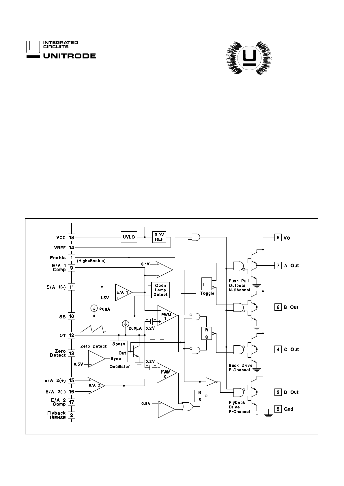
BLOCK DIAGRAM
• 1µA ICC when Disabled
• PWM Control for LCD Supply
• Zero Voltage Switched (ZVS) on
Push-Pull Drivers
• Open Lamp Detect Circuitry
• 4.5V to 20V Operation
• Non-saturating Transformer
Topology
• Smooth 100% Duty Cycle on
Buck PWM and 0% to 95% on
Flyback PWM
The UC1871 Famil y of IC’s is optimized for highly efficient fl uorescent lamp
control. An additional PWM controller is integrated on the IC for applications requiring an additional suppl y, as in LCD displays . When disabled the IC draws
only 1µA, providing a true disconnect feature, which is optimum for battery
powered systems. The switching frequency of all outputs are synchronized to
the resonant frequency of the e xternal passive network, which provides Zero
V oltage Switching on the Push-Pull drivers.
Soft-Start and open lamp detect circuitry have been incorporated to minimize
component stress. An open lamp i s detected on the compl etion of a soft-start
cycle.
The Buck control ler is optimized for smooth duty cycle control to 100%, while
the flyback control ensures a maximum duty cycle of 95%.
Other features include a precision 1% reference, under voltage lockout, flyback
current limit, and accurate minimum and maximum frequency control.
Resonant Fluorescent Lamp Driver
FEATURES
DESCRIPTION
UDG-92061-1
UC1871
UC2871
UC3871
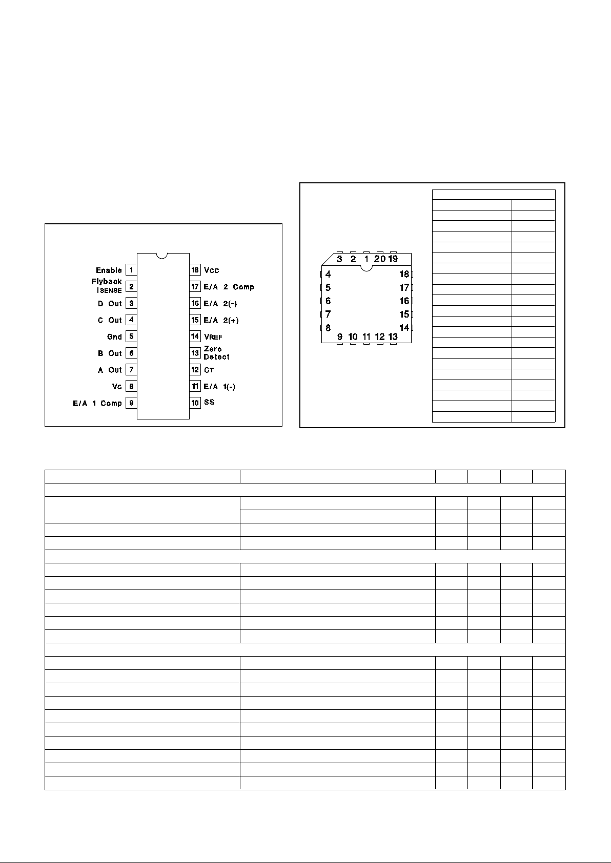
Note: Pin number s refer to DIL- 18 an d SOIC- 18 pa ckag es only.
PARAMETER TEST CONDITION S MIN TYP MAX UNITS
Reference Sect ion
Output Voltage T
J=25°C 2.963 3.000 3.037 V
Overtemp 2.940 3.000 3.060 V
Line Regulation V
CC = 4.75V to 18V 10 mV
Load Regulat io n Io=0 to -5mA 10 mV
Oscillator Section
Free Running Freq T
J=25°C 576878kHz
Max Sync Frequency T
J=25°C 160 200 240 kHz
Charge Curr ent V
CT = 1.5V 180 200 220 µA
Voltage Sta bi lity 2%
Temperature Stability 48%
Zero Detect Threshold 0.46 0.5 0.56 V
Error Amp 1 Sectio n
Input Voltage V
O = 2V 1.445 1.475 1.505 V
Input Bias Current -0.4 -2 µA
Open Loo p Ga in V
O = 0.5 to 3V 65 90 dB
Output High V
EA(-) = 1.3V 3.1 3.5 3.9 V
Output Low V
EA(-) = 1.7V 0.1 0.2 V
Output Source Current V
EA(-) = 1.3V, Vo = 2V -350 -500 µA
Output Sink Current V
EA(-) = 1.7V, Vo = 2V 10 20 mA
Common Mode Range 0V
IN-1V V
Unity Gain Bandwidth T
J = 25°C (Note 4) 1 MHz
Maximum Source Im peda nce Note 5 100k Ω
UC1871
UC2871
UC3871
ELECTRICAL CHARACTERIST ICS
Unless otherwise stated , thes e par am eters apply f or TA = -55°C to +125°C for the
UC1871; -25°C to +85°C for the UC2 871; 0°C t o +70°C f or the UC3871; V
CC = 5V,
V
C = 15V, VENABLE = 5V, CT = 1nF , Z ero Det = 1V.
ABSOLUTE MAXIMUM RATINGS
Analog Inputs . . . . . . . . . . . . . . . . . . . . . . . . . −0.3 to +10V
V
CC, VC Voltage . . . . . . . . . . . . . . . . . . . . . . . . . . . . . +20V
Zero Detect I nput Current
High Impedanc e Source . . . . . . . . . . . . . . . . . . +10mA
Zero Detect
Low Impedance Source. . . . . . . . . . . . . . . . . . . . . +20V
Power Dissipation at T
A = 25°C . . . . . . . . . . . . . . . . . . . 1W
Storage T e mperature. . . . . . . . . . . . . . . . -65 °C to +150°C
Lead Temp erature . . . . . . . . . . . . . . . . . . . . . . . . . . 300°C
Note 1: Current s are pos itive int o, nega tive out of the sp ecif ied te rminal.
Note 2: Consult Packaging Sec tion of Databook f or therma l
limitations and considerations of package.
DIL-18, SOIC-18 ( TOP VIEW)
J or N, DW Package
PACKAGE PIN FUNCTION
FUNCTION PIN
Gnd 1
B Out 2
A Out 3
VC 4
E/A 1 Comp 5
SS 6
E/A 1(-) 7
N/C 8
C
T 9
Zero Detect 10
N/C 11
VREF 12
E/A 2(+) 13
E/A 2(-) 14
E/A 2 Comp 15
V
CC 16
Enable 17
Flyback I
SENSE 18
D Out 19
C Out 20
PLCC-20 (Top View)
Q Package
CONNECTION DIAG RAMS
2
PARAMETER TEST CONDITION S MIN TYP MAX UNITS
Open Lamp Det ect Sect io n
Soft Start Threshold V
EA(-) = 0V 2.9 3.4 3.8 V
Error Amp Thresho ld V
SS = 4.2V 0.7 1.0 1.3 V
Soft S tart Curren t V
SS = 2V 10 20 40 µA
Error Amp 2 Sectio n
Input Offset Voltage V
O = 2V 0 10 mV
Input Bias Current -0.2 -1 µA
Input Offset Current 0.5 µA
Open Loo p Ga in V
O = 0.5 to 3V 65 90 dB
Output High V
ID = 100mV, VO = 2V 3.6 4 4.4 V
Output Low V
ID = -100mv, VO = 2V 0.1 0.2 V
Output Source Current V
ID = 100mV, V O = 2V -350 -500 µA
Output Sink Current V
ID = -100mV, VO = 2V 10 20 mA
Common Mode Range 0V
IN-2V V
Unity Gain Bandwidth T
J = 25°C (Note 4) 1 MHz
Isense Sec tion
Threshold 0.475 0.525 0.575 V
Output Secti on
Output Low Level I
OUT = 0, Outputs A and B 0.05 0.2 V
I
OUT = 10mA 0.1 0.4 V
I
OUT = 100mA 1.5 2.2 V
Output High Level I
OUT = 0, Outputs C and D 14.7 14.9 V
I
OUT = -10mA 13.5 14.3 V
I
OUT = -100mA 12.5 13.5 V
Rise Time T
J = 25°C, Cl = 1nF(Note 4) 30 80 ns
Fall Time T
J = 25°C, Cl = 1nF(Note 4) 30 80 ns
Output Dynamics
Out A and B Duty Cycle 48 49.9 50 %
Out C Max Duty Cycle V
EA1(-) = 1V 100 %
Out C Min Duty Cycle V
EA1(-) = 2V 0 %
Out D Max Duty Cycle V
EA2(+)- VEA2(-) = 100mV 92 96 %
Out D Min Duty Cycle V
EA2(+)- VEA2(-) = -100mV 0 %
Under Voltage Lockout Section
Start-Up Th res hold 3.7 4.2 4.5 V
Hysterisis 120 200 280 mV
Enable Sect io n
Input High Threshold 2V
Input low Threshold 0.8 V
Input Current V
ENABLE = 5V 150 400 µA
Supply Cur ren t Sectio n
VCC Supply Current V
CC = 20V 8 14 mA
VC Supply Current V
C=20V 7 12 mA
ICC Disabled V
CC = 20V, VENABLE = 0V 1 10 µA
UC1871
UC2871
UC3871
ELECTRICAL
CHARACTERISTICS (cont.)
Unless otherwise stated , thes e par am eters apply f or TA = -55°C to +125°C for the UC1 871;
-25°C to +85°C for the UC2871; 0°C to +70°C for the UC3871; V
CC = 5V, VC = 15V,
V
ENABLE = 5V, CT = 1nF, Zero Det = 1V.
Note 3: Unless otherwise sp ecif ie d, all voltage s are with re spec t to ground .
Currents are positive into, and negat ive out of the specified terminal.
Note 4: Guaranteed by design but not 100% tested in production.
Note 5: Impedance below spe cified maximum guaran te es proper oper at ion of the O pen La mp Dete ct.
3

Figure 1
UC1871
UC2871
UC3871
Figure 1 shows a complete application circuit using the
UC3871 Resonant Fluorescent lamp and LCD driver.
The IC provides all drive, control and housekeeping functions to implement CCFL and LCD converters. The buck
output voltage (transformer center-tap) provides the zero
crossing and synchronization signal. The LCD supply
modulator is also synchronized to the resonant tank.
The buck modulator drives a P-channel MOSFET directly , and operates over a 0-100% duty-cycle range. The
modulation range includes 100%, allowing operation with
minimal head room. The LCD supply modulator also directly drives a P-channel MOSFET, but it’s duty-cycle is
limited to 95% to prevent flyback supply foldback.
The oscillator and synchro nization circuitry are shown in
Figure 2. The oscillator is designed to synchronize over a
3:1 frequency range. In an actual application however,
the frequency range is only about 1.5:1. A zero detect
comparator senses the primary center-tap voltage, generating a synchronization pulse when the resonant waveform falls to zero. The actual threshold is 0.5 volts,
providing a smal l amount of anti cipation to offset propagation delay .
The synchronization pulse width is the time that the 4mA
current sink takes to discharge the timing capacitor to 0.1
volts. This pulse width sets the LCD supply modulator
minimum off time, and also limits the minimum linear
control range of th e buck modulator. The 200µA current
source charges the capacitor to a maximum of 3 volts. A
comparator blanks the zero detect signal until the capacitor voltage exceeds 1 volt, preventing multiple synchronization pulse generation and setting the maximum
frequency. If the capacitor voltage reaches 3 volts (a zero
detection has not occurred) an internal clock pulse is
generated to limit the minimum frequency.
TYPICAL APPLICATION
APPLICATION INFORMATION
4
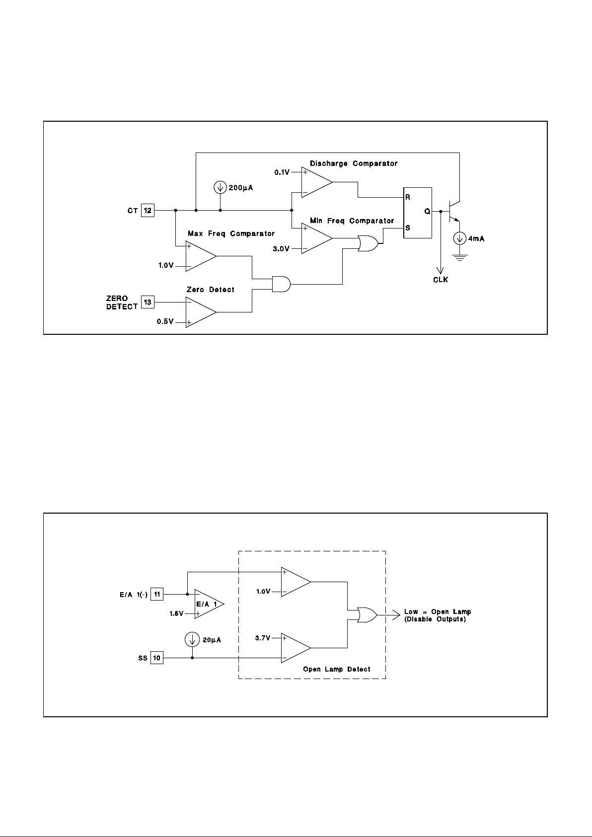
A unique protection feature incorporated in the UC3871
is the Open Lamp Detect circuit. An open lamp interrupts
the current feedback loop and causes very high secondary voltage. Operation in this mode will usually breakdown the transformer’s insulation, causing permanent
damage to the converter. The open lamp detect circuit,
shown in Figure 3 senses the lamp current feedback signal at the error amplifiers input, and shuts down the outputs if insufficient signal is present. Soft-start circuitry
limits initial turn-on cu rrents and blanks the open lamp
detect signal.
Other features are included to minimize external circuitry
requirements. A logic level enable pin shuts down the IC,
allowing direct connection to the battery. During shutdown, the IC typically draws less than 1µA. The UC3871,
operating from 4.5V to 20V, is compatible with almost all
battery voltages used in portable computers. Under-voltage lockout circuitry disables operation until sufficient
supply voltage is available, and a 1% voltage reference
insures accurate opera tion. Both inputs to the LCD supply error amplifie r are uncommitted, allowing positive or
negative supply loop closure without additional circuitry.
The LCD supply modulator also incorporates cycle-bycycle current limiting for added protection.
Figure 3
UC1871
UC2871
UC3871
UNITRODE INTEGRATED CIRCUITS
7 CONTINENTAL BLVD. • MERRIMACK, NH 03054
TEL. (603) 424-2410 • FAX (603) 424-3460
APPLICATION INFORMATION (cont.)
Figure 2
UC1871 Open Lamp Detect Circuitry
UC3871 Oscillator Section
5

IMPORTANT NOTICE
T exas Instruments and its subsidiaries (TI) reserve the right to make changes to their products or to discontinue
any product or service without notice, and advise customers to obtain the latest version of relevant information
to verify, before placing orders, that information being relied on is current and complete. All products are sold
subject to the terms and conditions of sale supplied at the time of order acknowledgement, including those
pertaining to warranty, patent infringement, and limitation of liability.
TI warrants performance of its semiconductor products to the specifications applicable at the time of sale in
accordance with TI’s standard warranty. Testing and other quality control techniques are utilized to the extent
TI deems necessary to support this warranty. Specific testing of all parameters of each device is not necessarily
performed, except those mandated by government requirements.
CERT AIN APPLICATIONS USING SEMICONDUCTOR PRODUCTS MA Y INVOLVE POTENTIAL RISKS OF
DEATH, PERSONAL INJURY, OR SEVERE PROPERTY OR ENVIRONMENTAL DAMAGE (“CRITICAL
APPLICATIONS”). TI SEMICONDUCTOR PRODUCTS ARE NOT DESIGNED, AUTHORIZED, OR
WARRANTED TO BE SUITABLE FOR USE IN LIFE-SUPPORT DEVICES OR SYSTEMS OR OTHER
CRITICAL APPLICATIONS. INCLUSION OF TI PRODUCTS IN SUCH APPLICA TIONS IS UNDERSTOOD T O
BE FULLY AT THE CUSTOMER’S RISK.
In order to minimize risks associated with the customer’s applications, adequate design and operating
safeguards must be provided by the customer to minimize inherent or procedural hazards.
TI assumes no liability for applications assistance or customer product design. TI does not warrant or represent
that any license, either express or implied, is granted under any patent right, copyright, mask work right, or other
intellectual property right of TI covering or relating to any combination, machine, or process in which such
semiconductor products or services might be or are used. TI’s publication of information regarding any third
party’s products or services does not constitute TI’s approval, warranty or endorsement thereof.
Copyright 1999, Texas Instruments Incorporated
 Loading...